I completed this part in Week-08 Electronic Design.
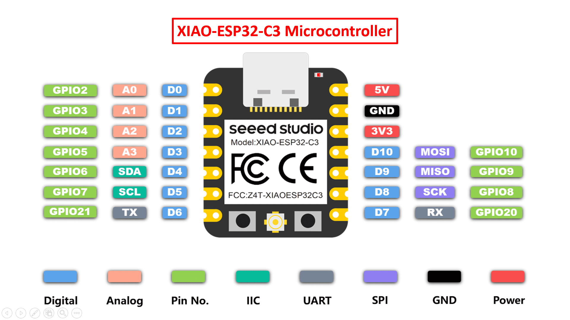
1) XIAO-ESP32-C3 microcontroller
2) Resistor
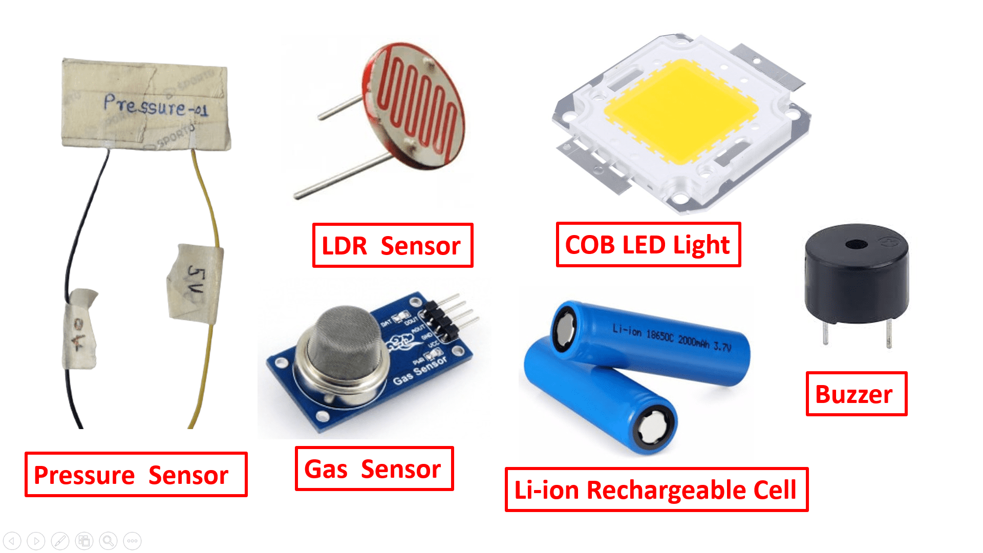
3) Pressure Sensor
4) MQ135 Gas Sensor
5) LDR Sensor
6) COB LED light
7) Buzzer
I used AutoDesk Eagle software to design my PCB board.

To create a new project, first go to the "File" which is located at the top-left side of the interface. Then, click on "New" and select "Project" to create a new blank projecct for our design work.
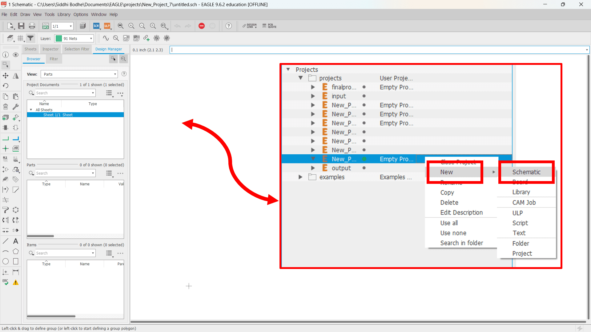
Now, a dropdown list of created project files is open. Click on "New" and select the "Schematic" to design the connecction diagram. Here, a new window is opened after hitting on "Schematic" option to design the PCB Schematic.

To design the PCB schematic, I have installed some libraries (connectors, resistors, switches, microcontroller,etc.) just by opening the library manager and adding the required libraries into the software.
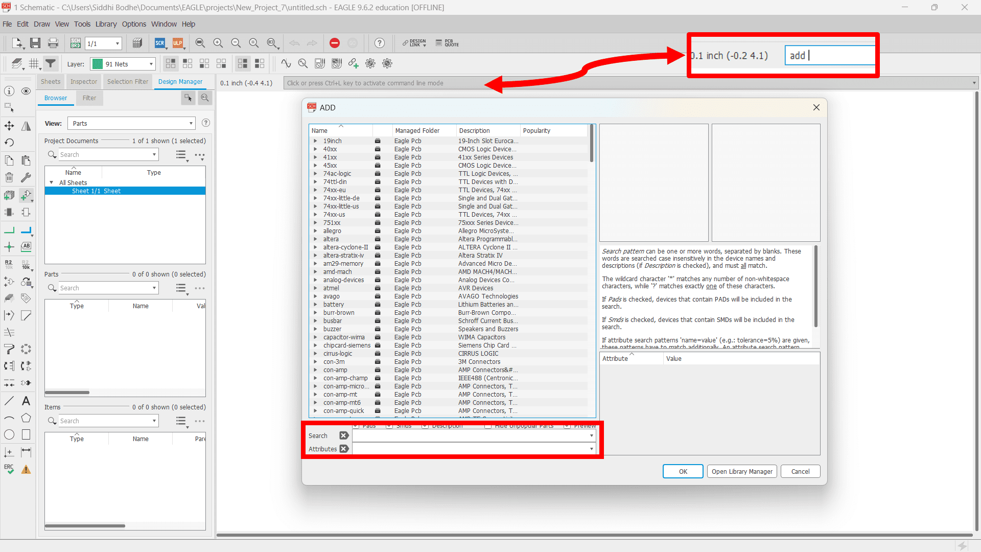
After the library installation process, I inserted all the electronic components that I want to use for my Final Project by typing "add" + Enter on command line at the header.
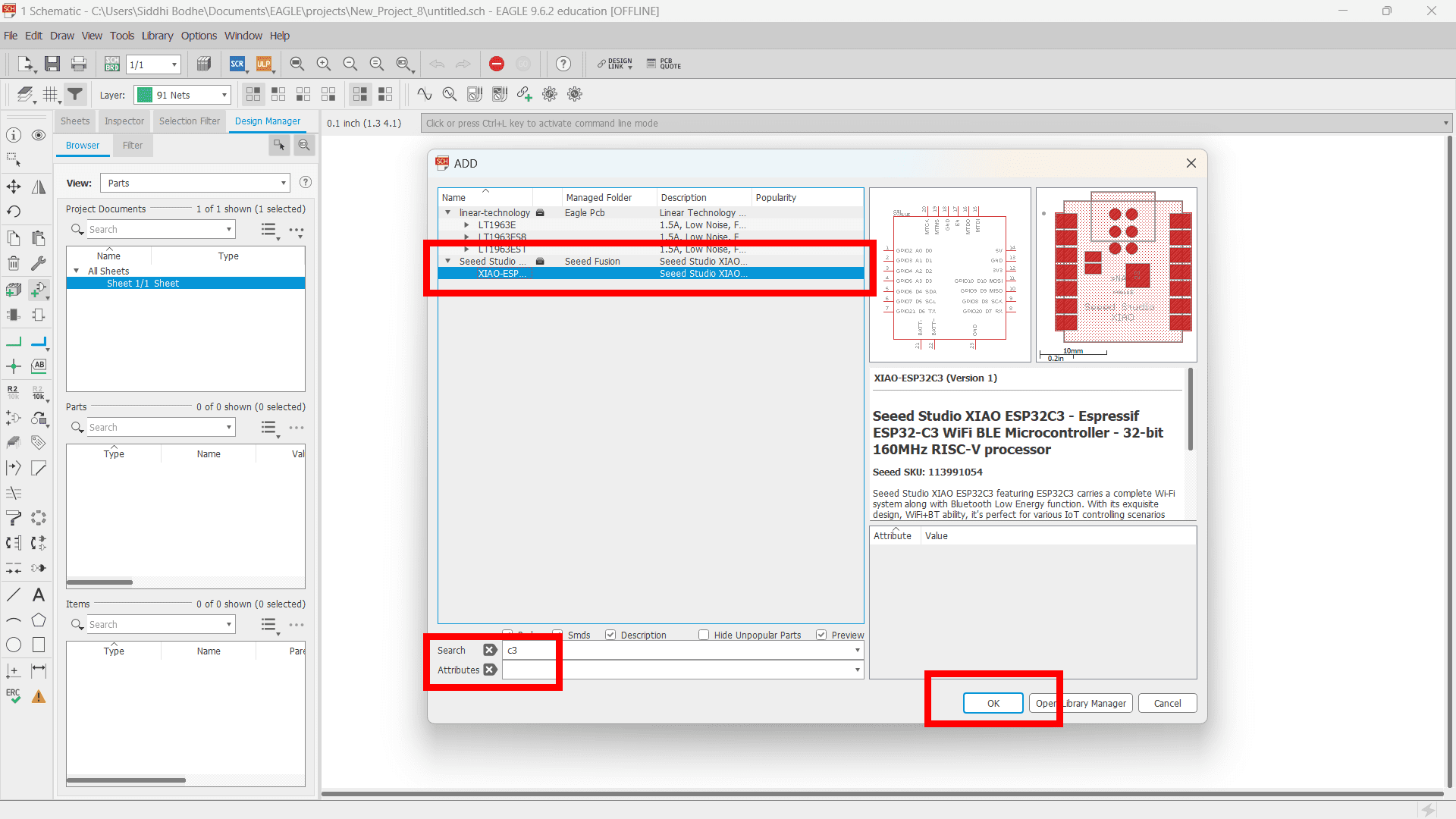
Here, I inserted XIAO-ESP32-C3 microcontroller using the same above process. Likewise, I inserted resistor, 2 pin connector, 4 pin connector in my schematic.
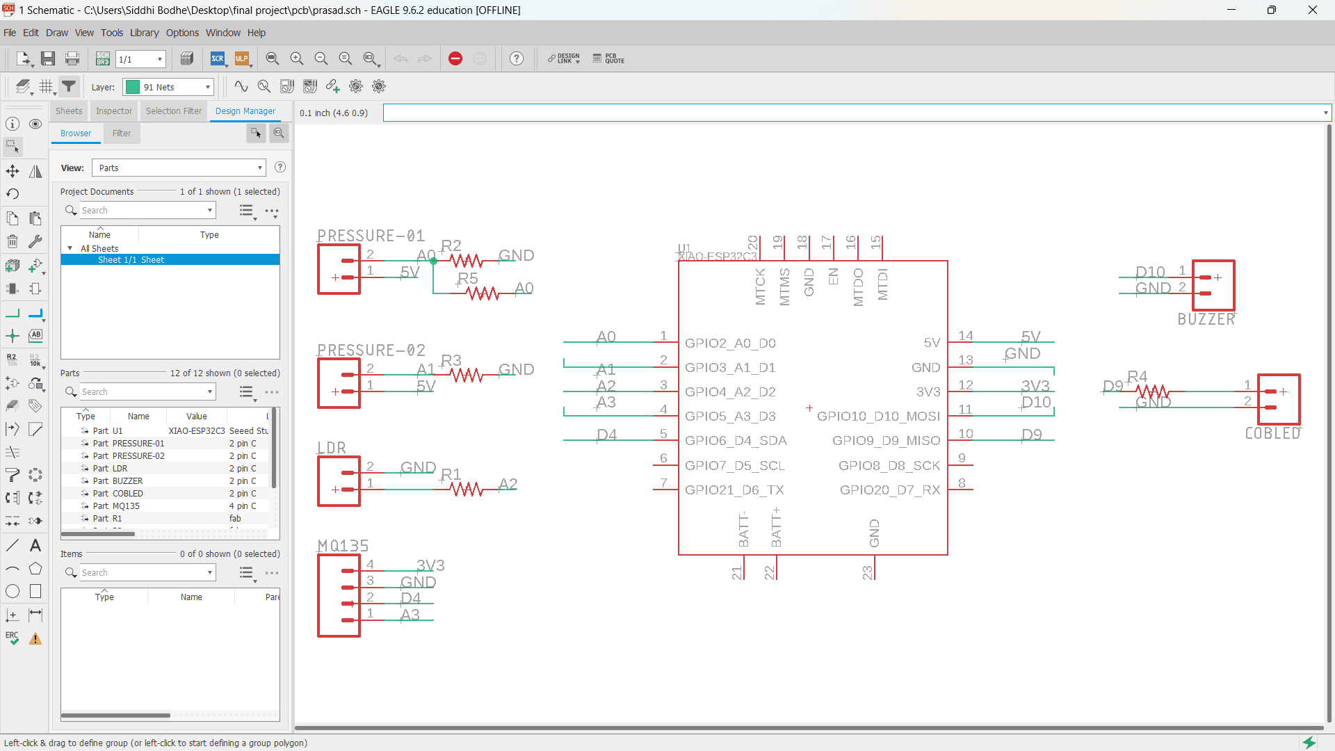
In schematic design, I used "select", "move", "rotate", "label", "route wire" commands to design the whole schematic of PCB board.

In board design, I used "select", "move", "rotate", "route wire of 16 mills" commands to designn my complete board same as schematic part.
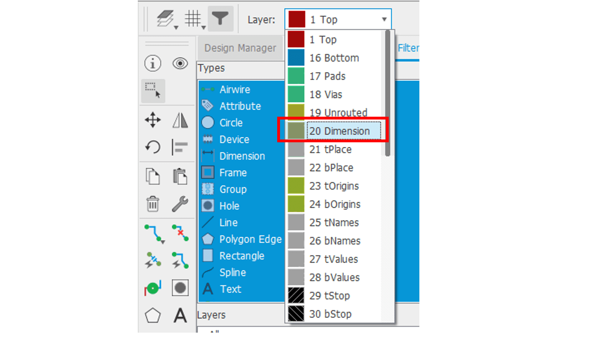
Then, select "20 dimension" layer from layer dropdown list to draw outline of the PCB board.
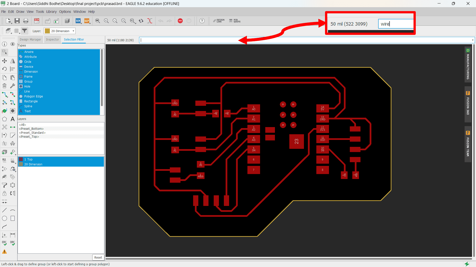
Here, again type "wire" in the command line to dtaw outline of PCB board. Finally, PCB is ready!

Now, I wanted to export separate PNG images for traces and outline. So, here I selected only "Top" layer from layer settings menu.

Now, only "top" layer is visible. Go to "file" located at the header, click on "export" and select "image" option. And export the image as per your required settings includes resolution, monochrome, area, etc.
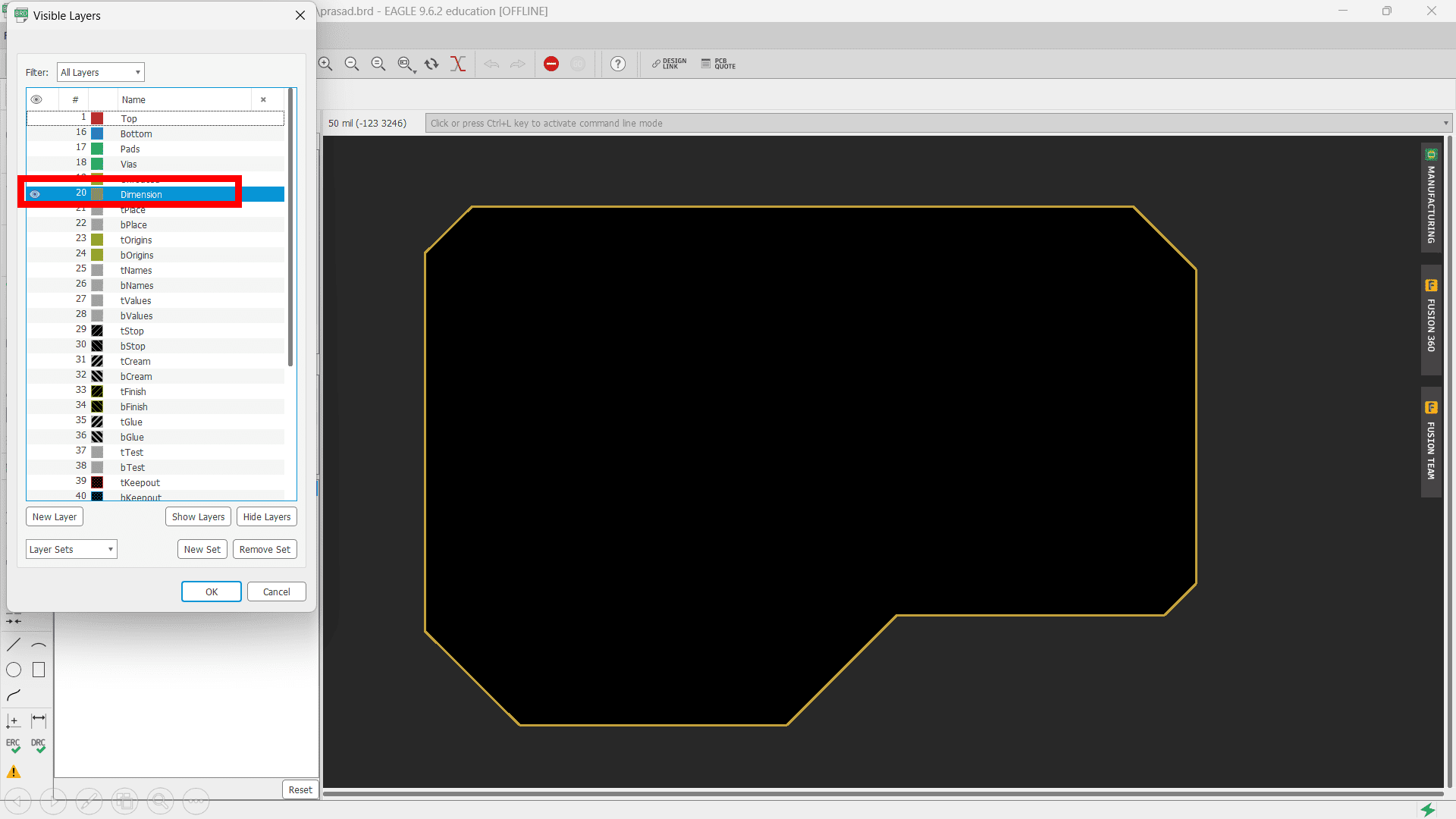
Now, select only "dimension" layer from layer setting to generate image of outline.
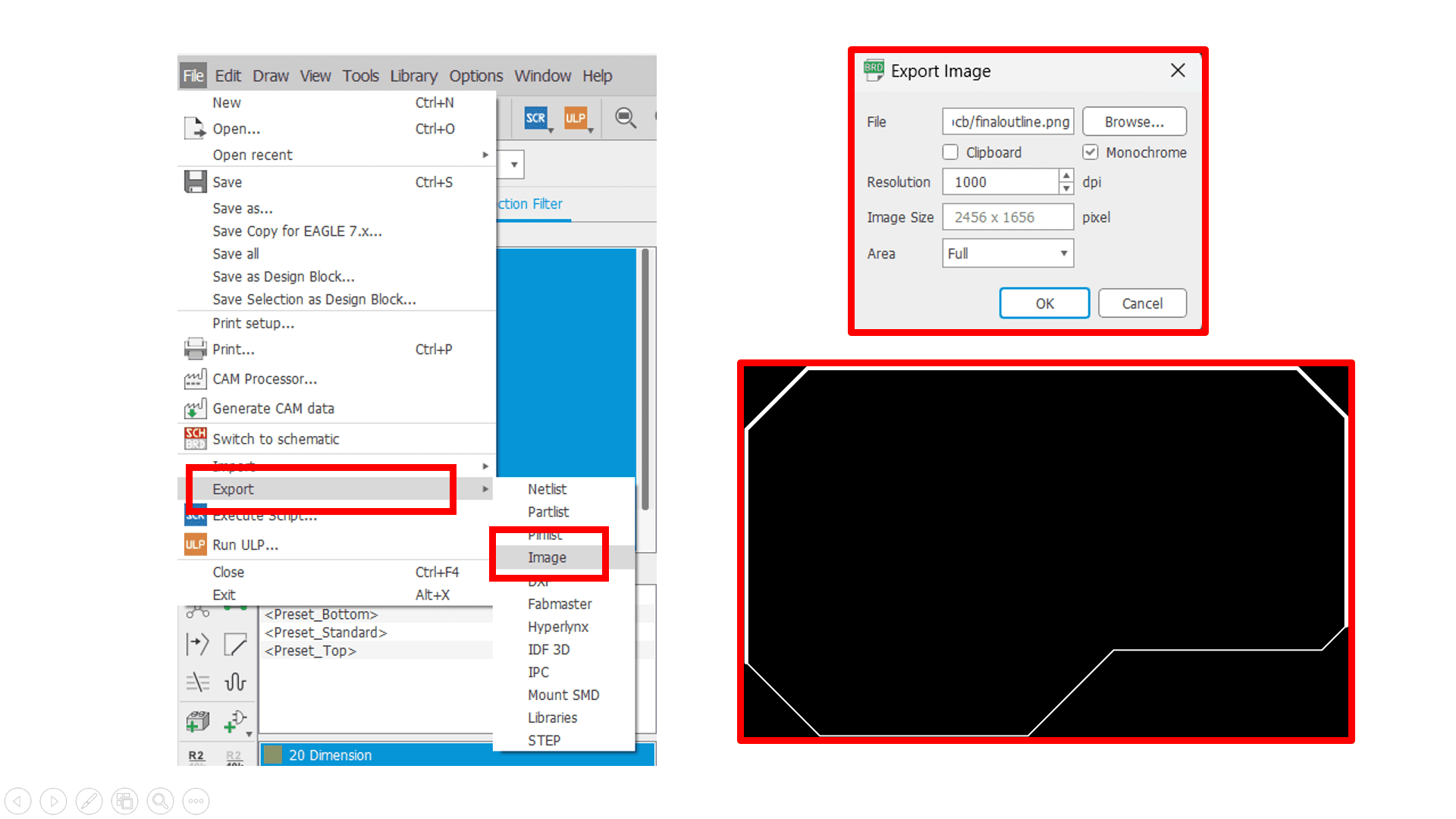
Again, use same process as traces to export the PNG immage of ouline.
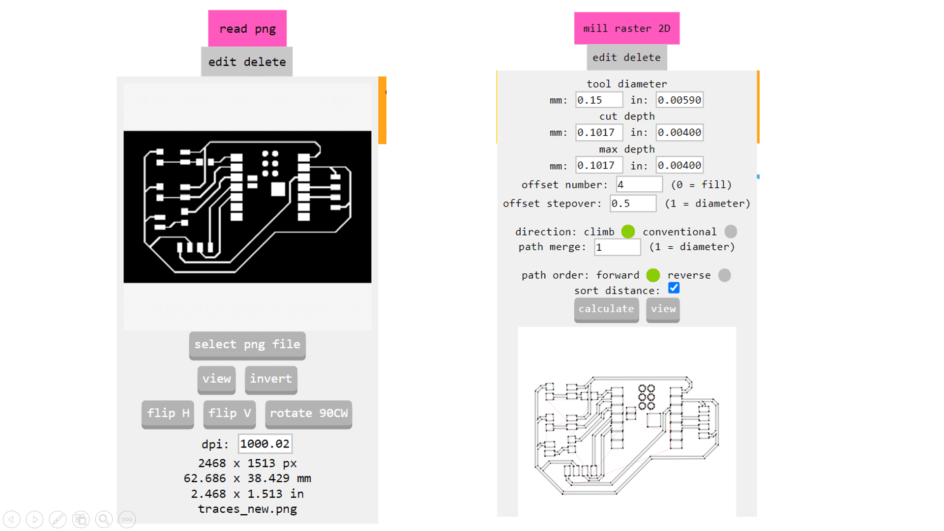
Now, I used MIT Mods CE to generate GCode of image for PCB Milling process by inserting required parameters such as tool diameter, depth of cut and offset nummber.
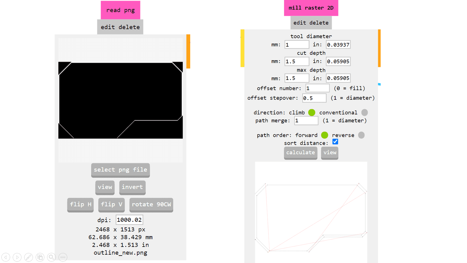
Again, use same process to generate GCode of outline of PCB.
Here is the video of PCB Milling process of my final project PCB.
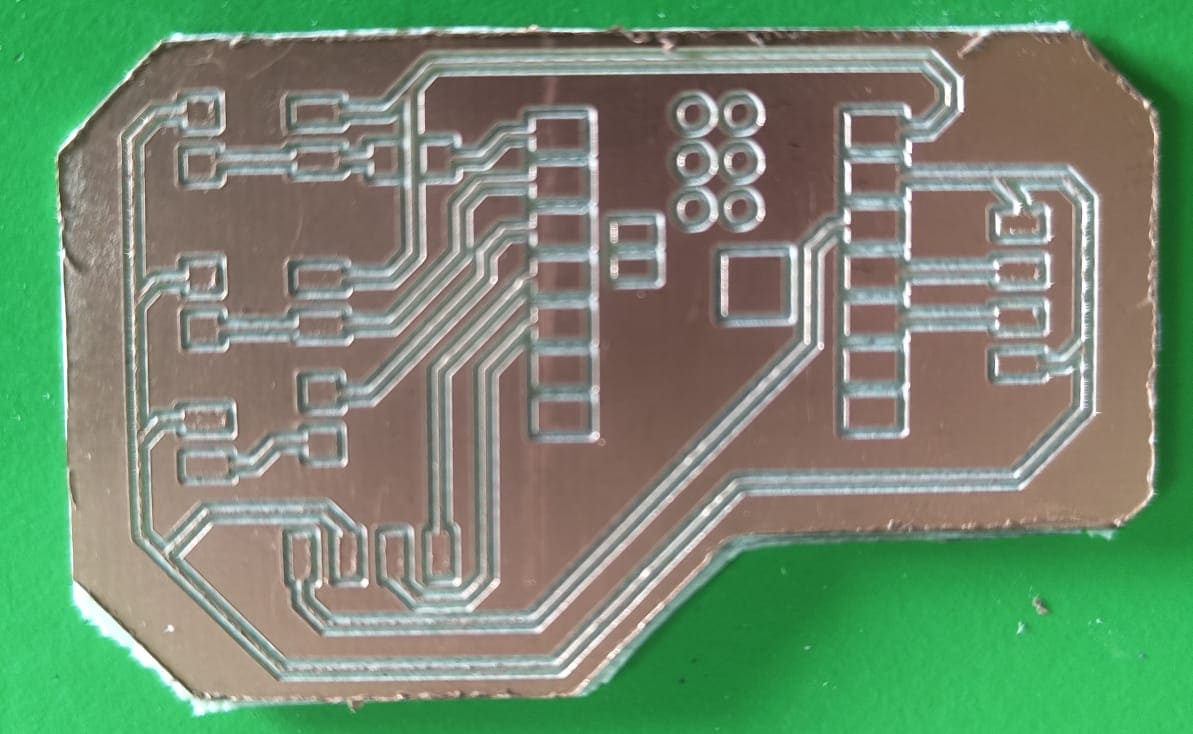
Here, I got the final output.
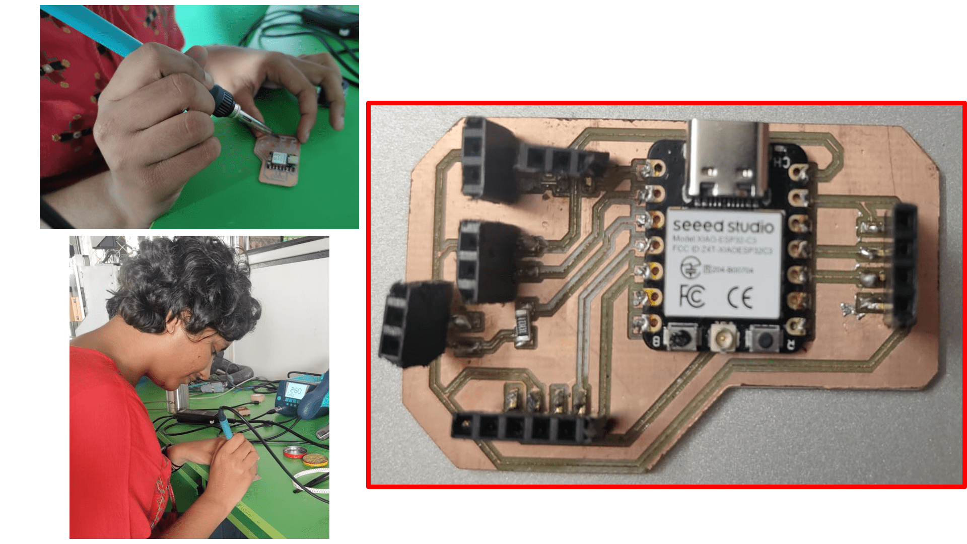
Then, I soldered my PCB Board and finally the board is ready.