Here is the link of Group Assignment Page
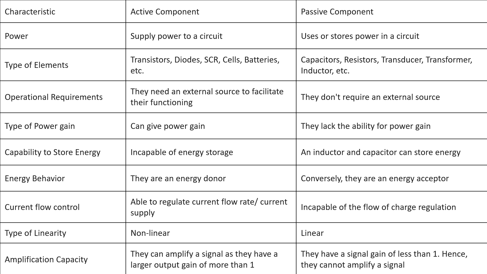
An electronic circuit is a system comprising various electronic components, like resistors, transistors, capacitors, inductors, and diodes, interconnected by conductive pathways. These pathways enable the flow of electric current. At least one active component, such as a transistor, is required for operation. Electronic circuits facilitate a range of functions, including signal amplification, computational operations, and data transfer between different points.
Ribbon Cable
Ribbon cable is also known as multi-wire planar cable, it is used in low voltage applications and high performance, space restricted applications.
It is a cable with many conducting wires are parallel to each other on the same plane, it results in wide and flat cable.
IDC connector
An insulation-displacement contact (IDC), also known as insulation-piercing contact (IPC) is an electrical connector designed to be connected to the conductor(s) of an insulated cable by a connection process which forces a selectively sharpened blade or blades through the insulation, bypassing the need to strip the conductors of insulation before connecting. When properly made, the connector blade cold-welds to the conductor, making a theoretically reliable gas-tight connection.
Buttons
Buttons are the type of switch, they acts like momentary triggers, when the button is pressed it completes the circuit, similar to closing a switch, allowing current to flow and activating the connected system. there is a spring to ensure the button automatically returns to its original off position once released.
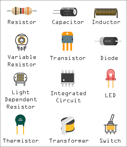
Resistor
Resistor is passive element, it has two terminals that implements electric resistance. Resistor is used to reduce current flow
This week, I've decided to create a PCB board for my hydroponics system project. I've utilized the Xiao ESP32-C3 IC and integrated it with an LED, a resistor, and a push button. Additionally, I've included an LCD display to show humidity and moisture levels, along with a DHT11 sensor for moisture detection.
"I have downloaded all the necessary libraries for my board design from the internet.
Here are the links-
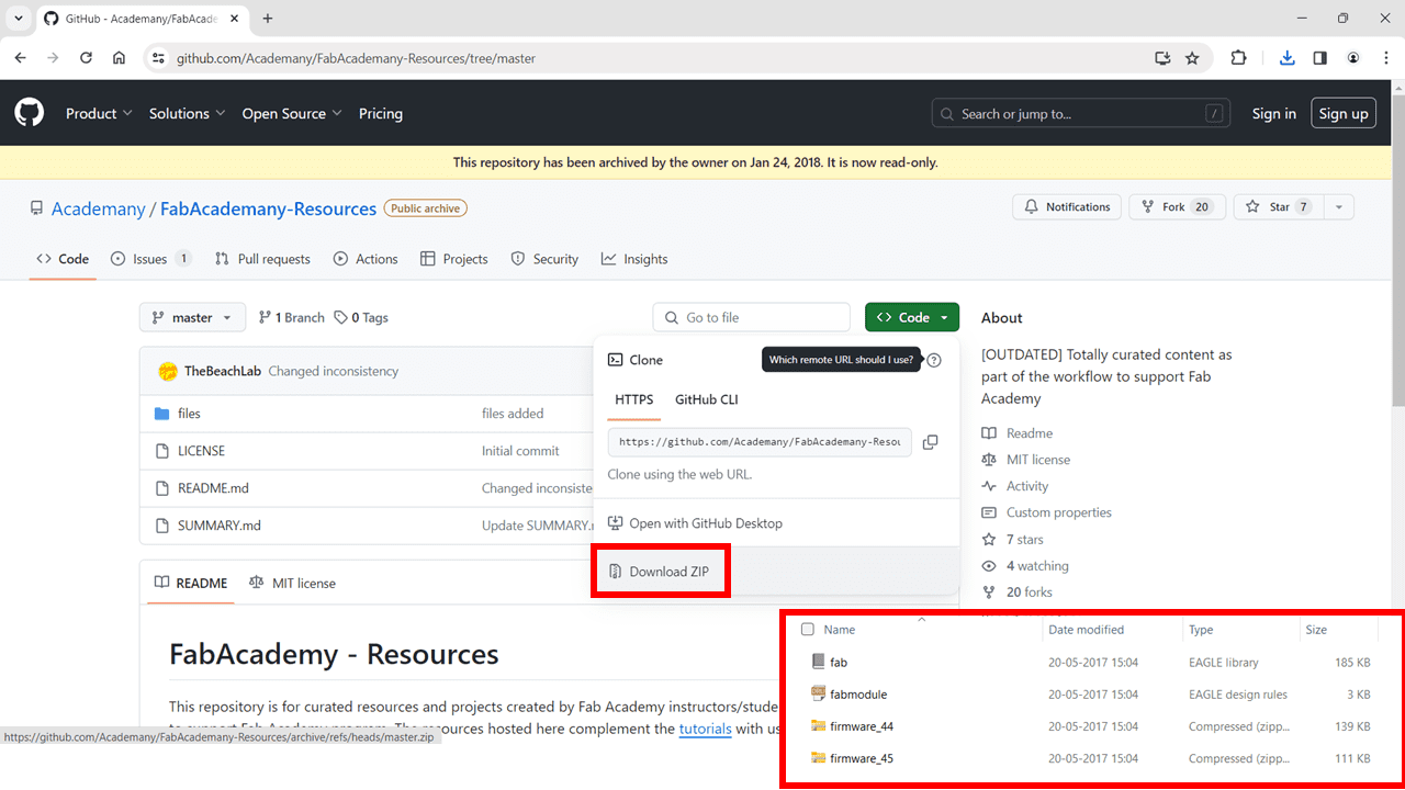
1. FabAcademany- Resources
2. Xiao Esp32 C3
3. Connectors-Sparkfun

I used the Autodesk Eagle For the design of the board
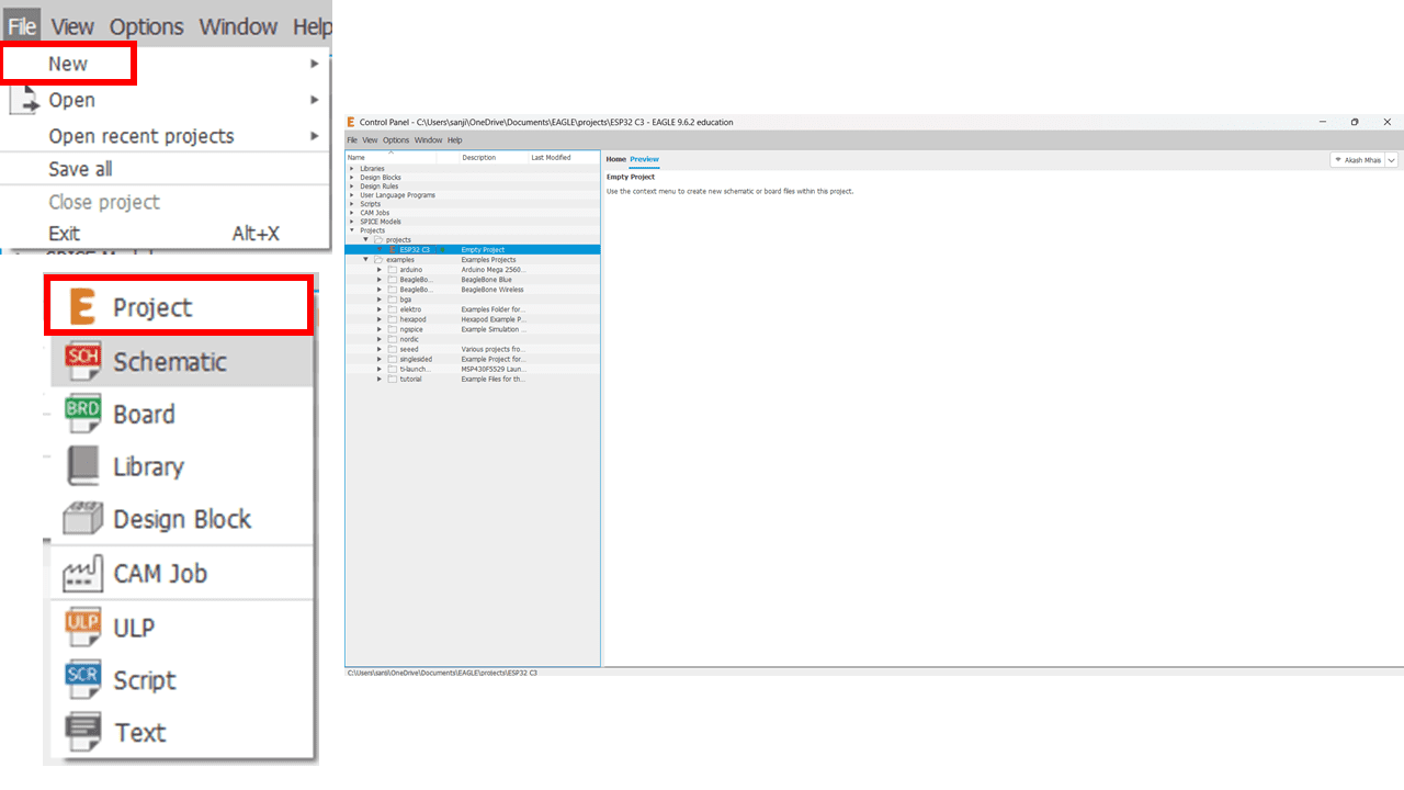
To create the schematic of the board, go to New --> Project. Then, right-click on it to change the project name, and set it as "ESP32 C3".
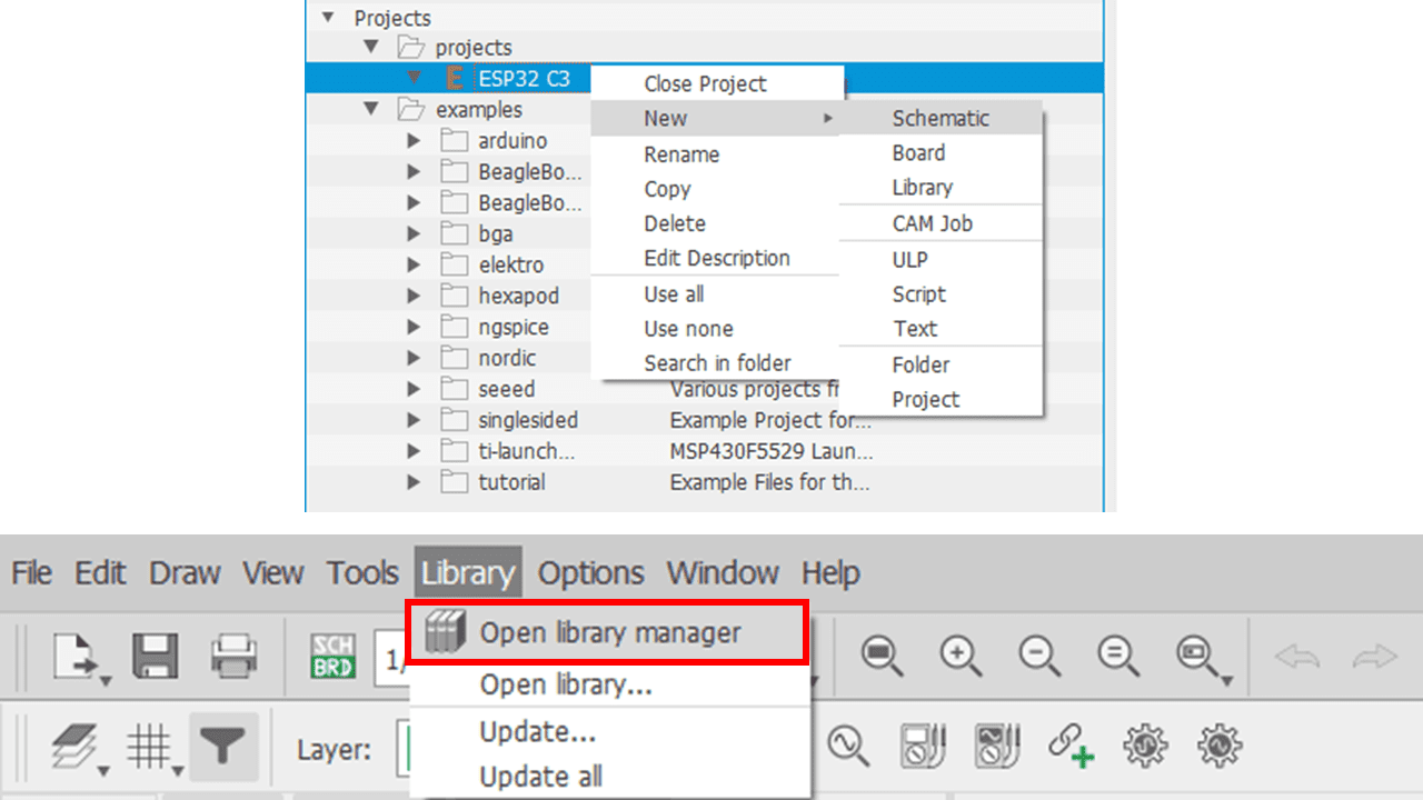
Right-click on the project, and then select New --> Schematic. This action will create a schematic window where we can draw the schematic. then go to Library and navigate to Open library manager.
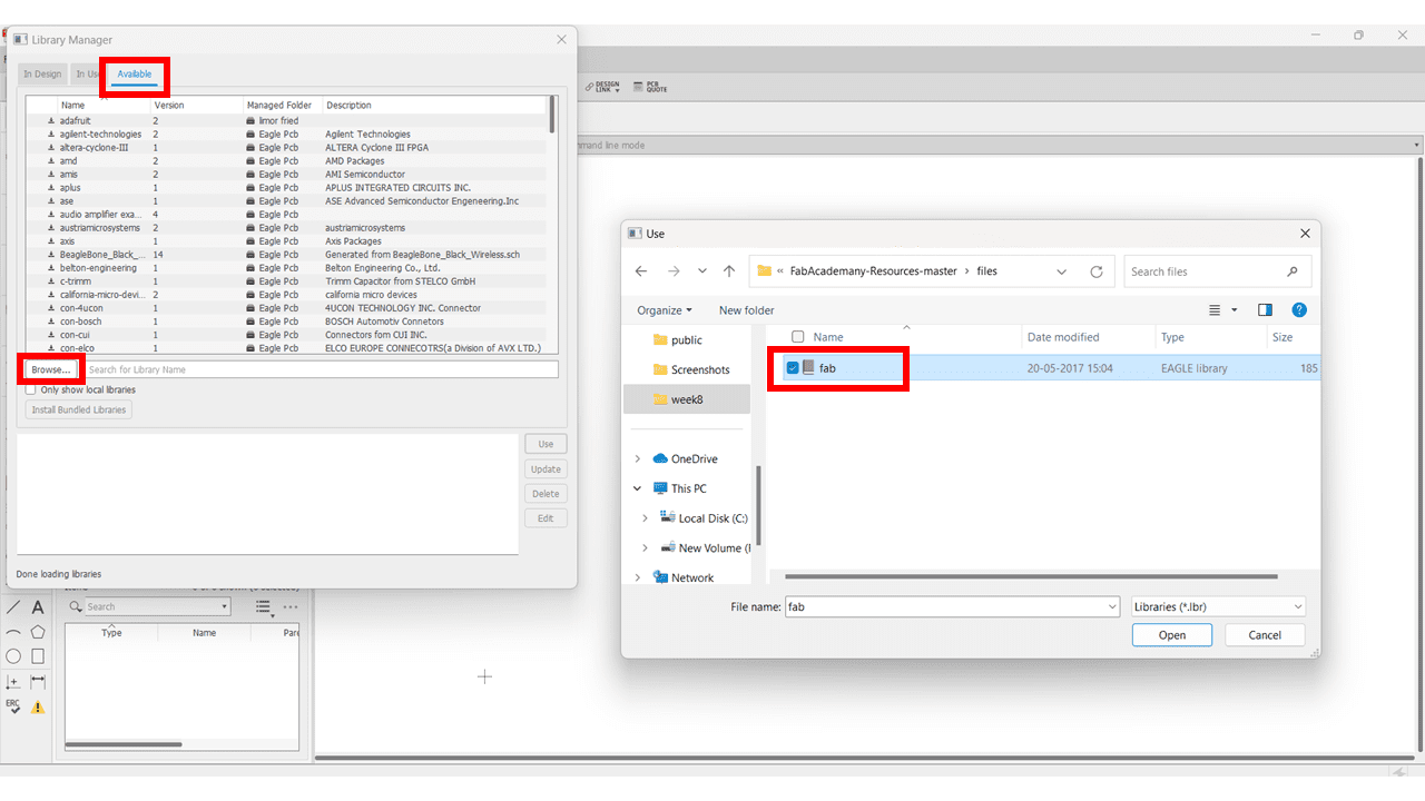
Click on the Available option, then using browse option select the file which is downloaded with extension .lbr
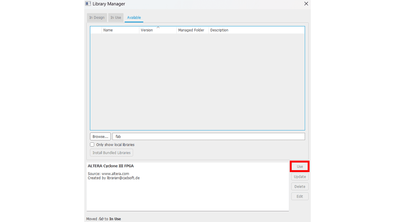
After fetching that library, click on the "Use" option to incorporate it into the board design.
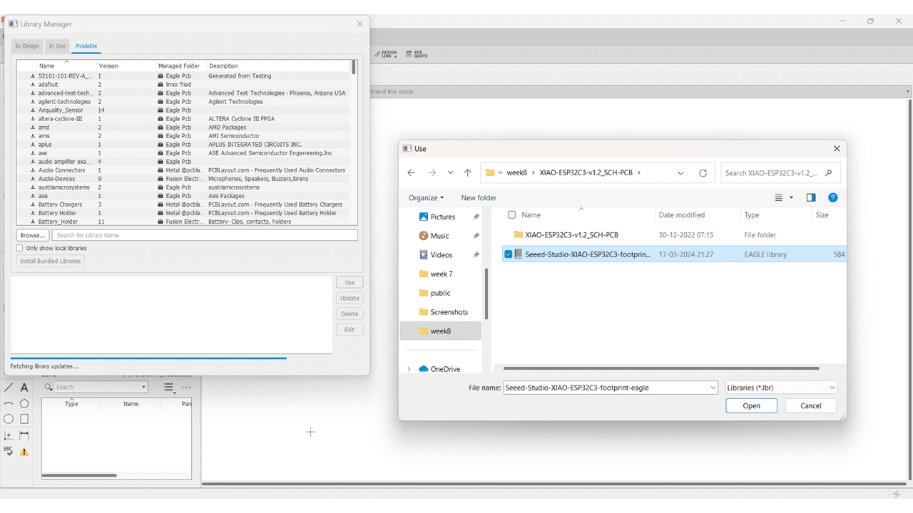
Similarly I done this for remaining libraries.
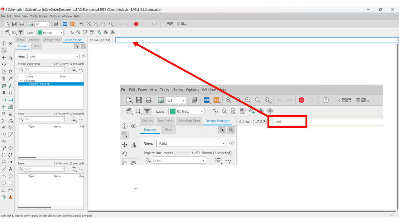
In the command line, type "add" to add the symbols of the components.
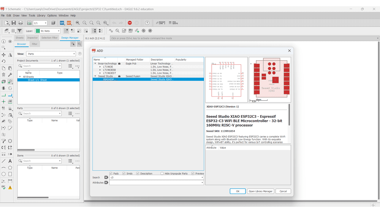
Search for "ESP32 C3" or "Xiao Boards" gor the board that we want to make.
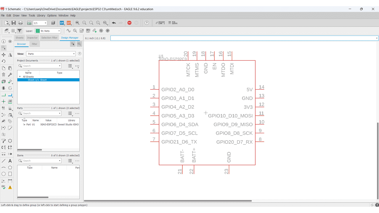
Here is the Schematic of the IC
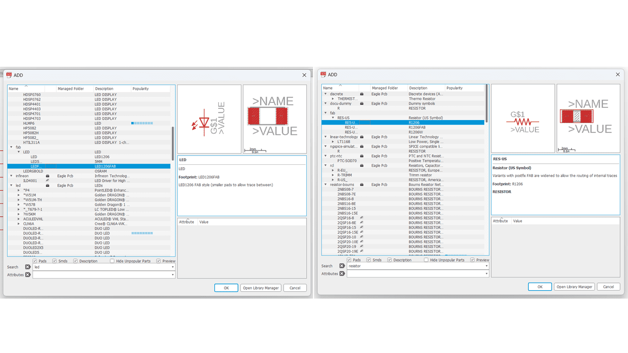
These LED's and the Resistors I used for my board
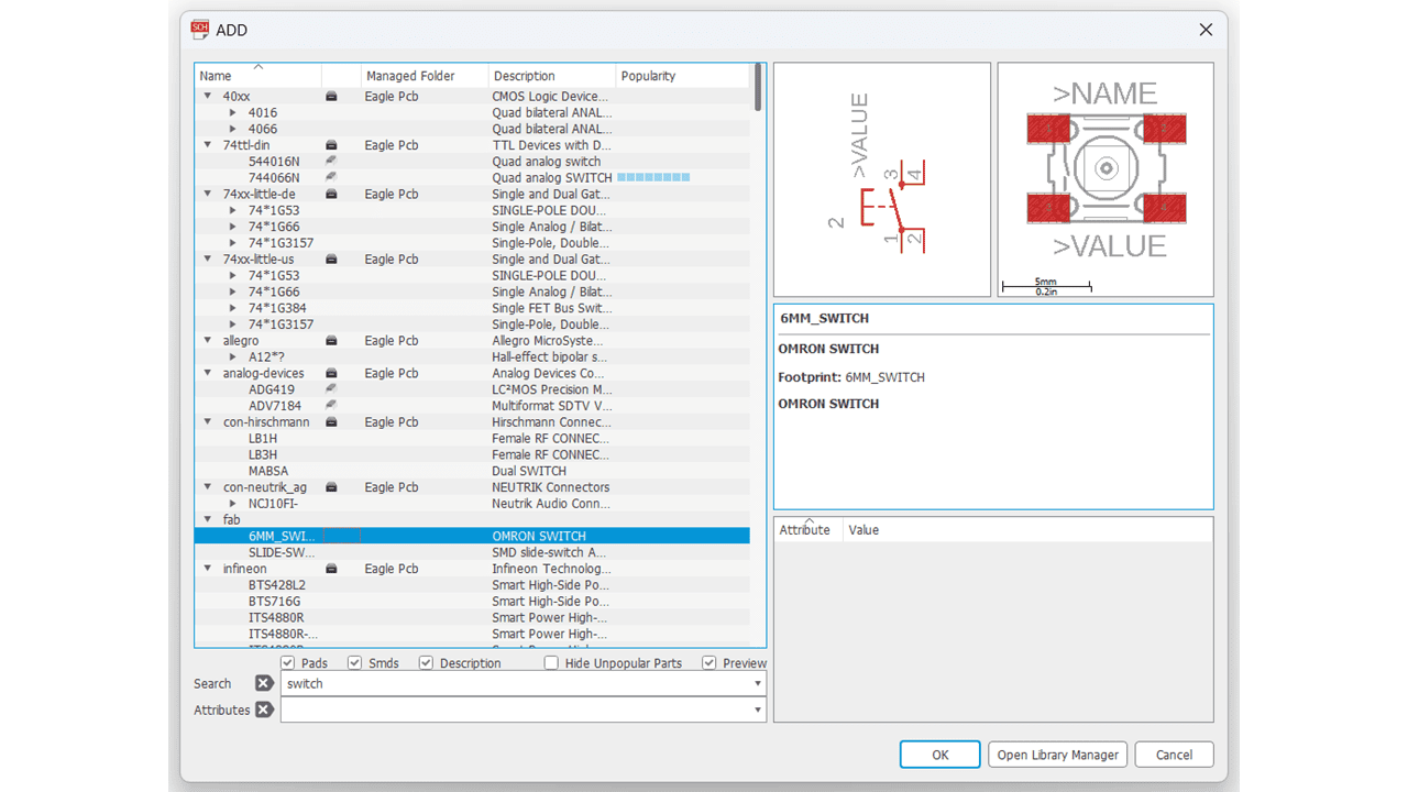
This Push button or the Switch I used from fab library.
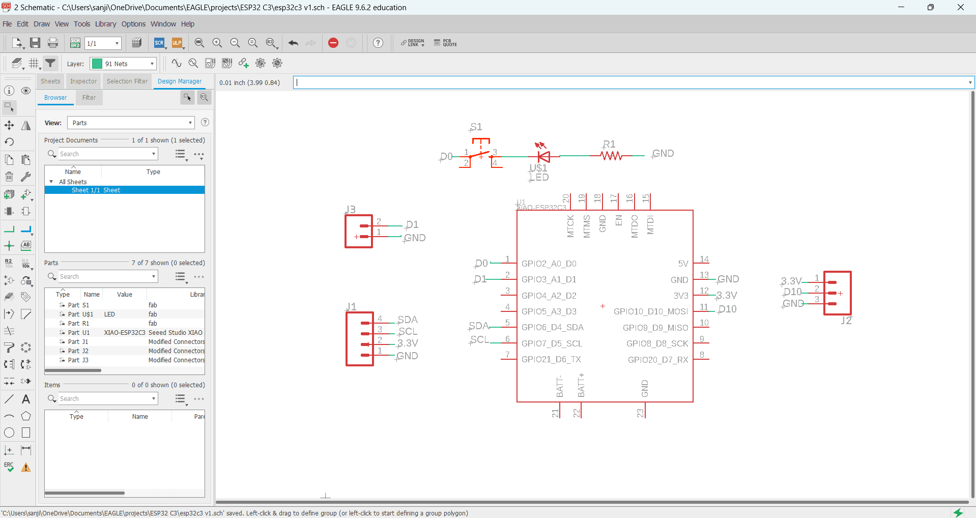
This is the final Schematic in which 1xLED, 1xResistor, 1xEsp32 C3, 1x2pin connector, 1x3pin connector, 1x4pin connector, 1xSwitch are the components.
Then i clicked on the Switch to Board option to design it.
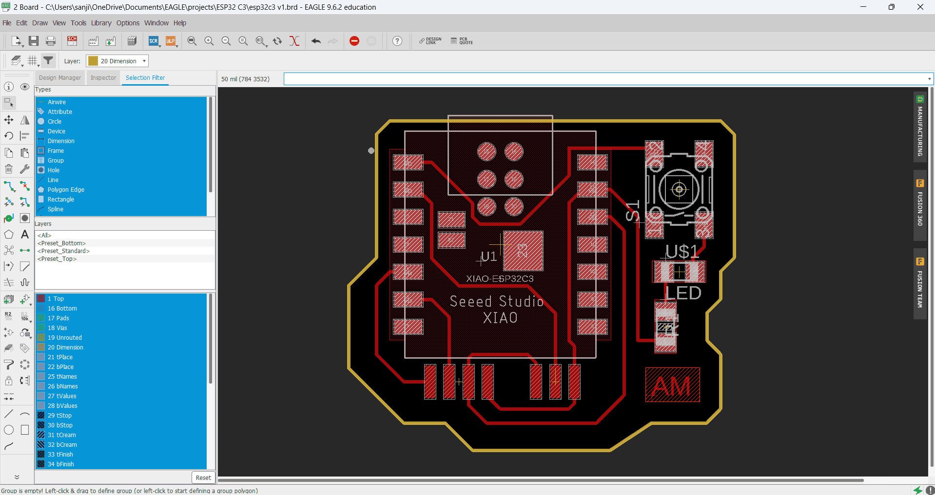
This is the final output I got after the designing of the board.
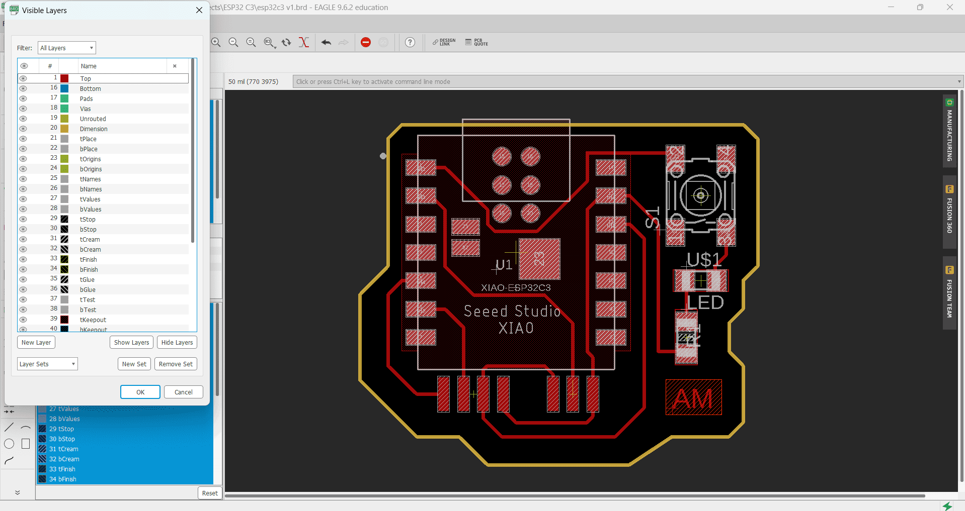
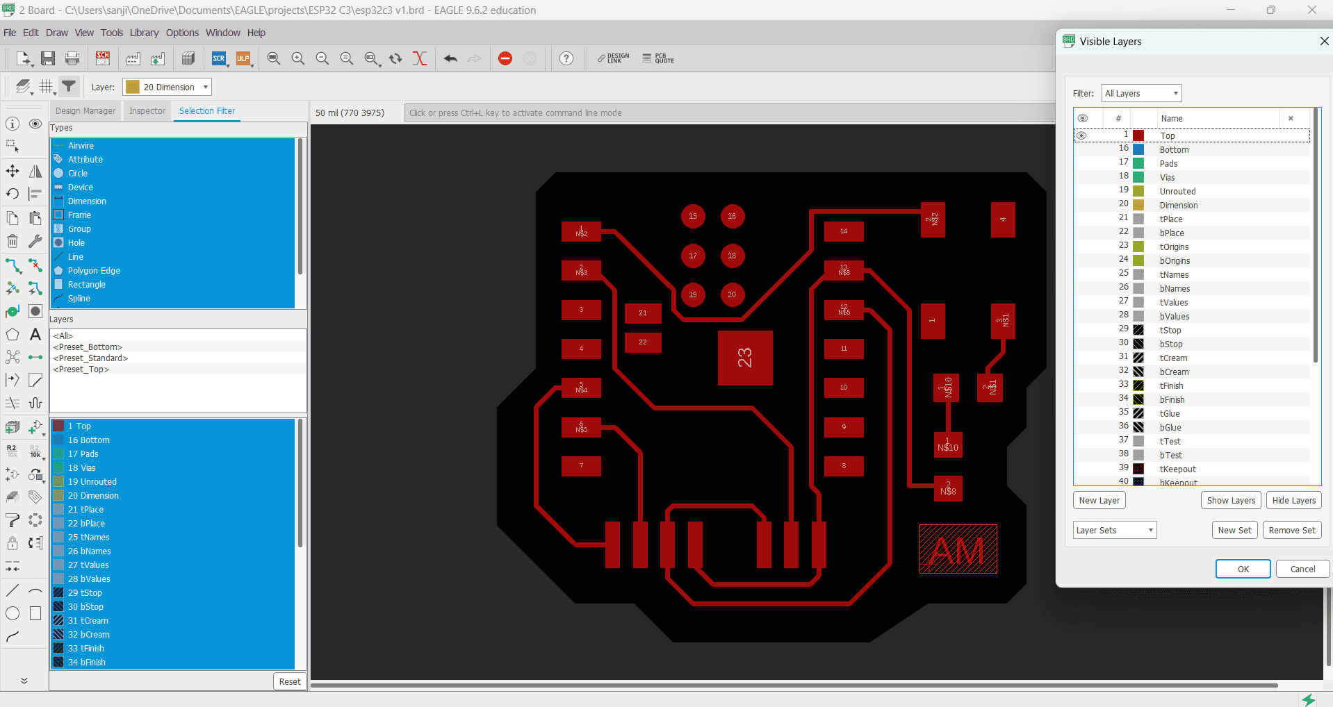
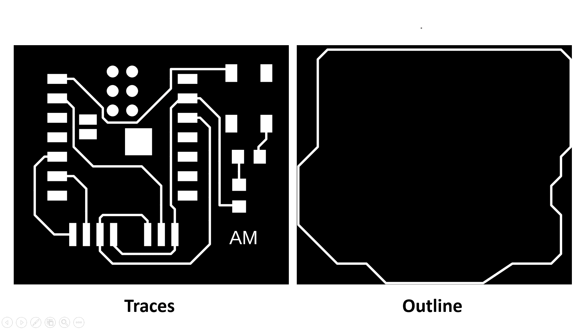
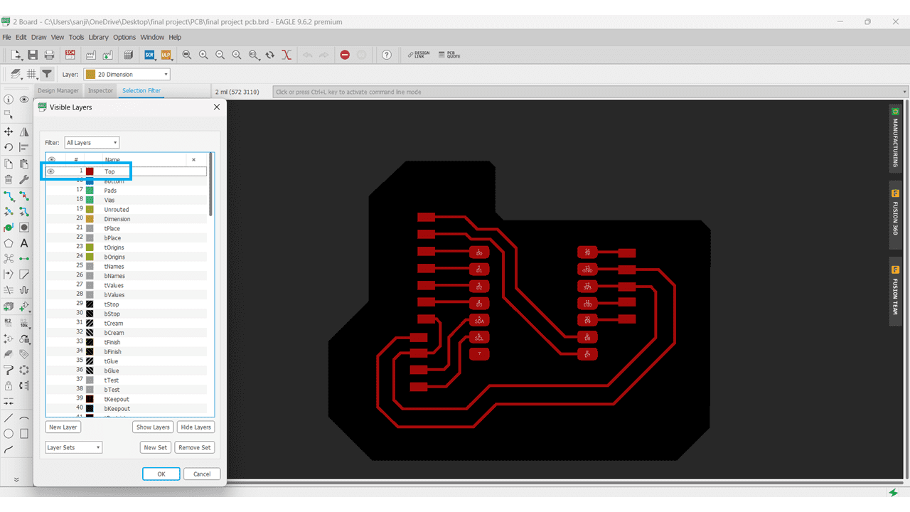
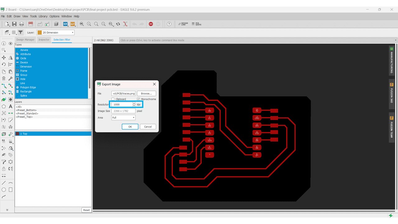
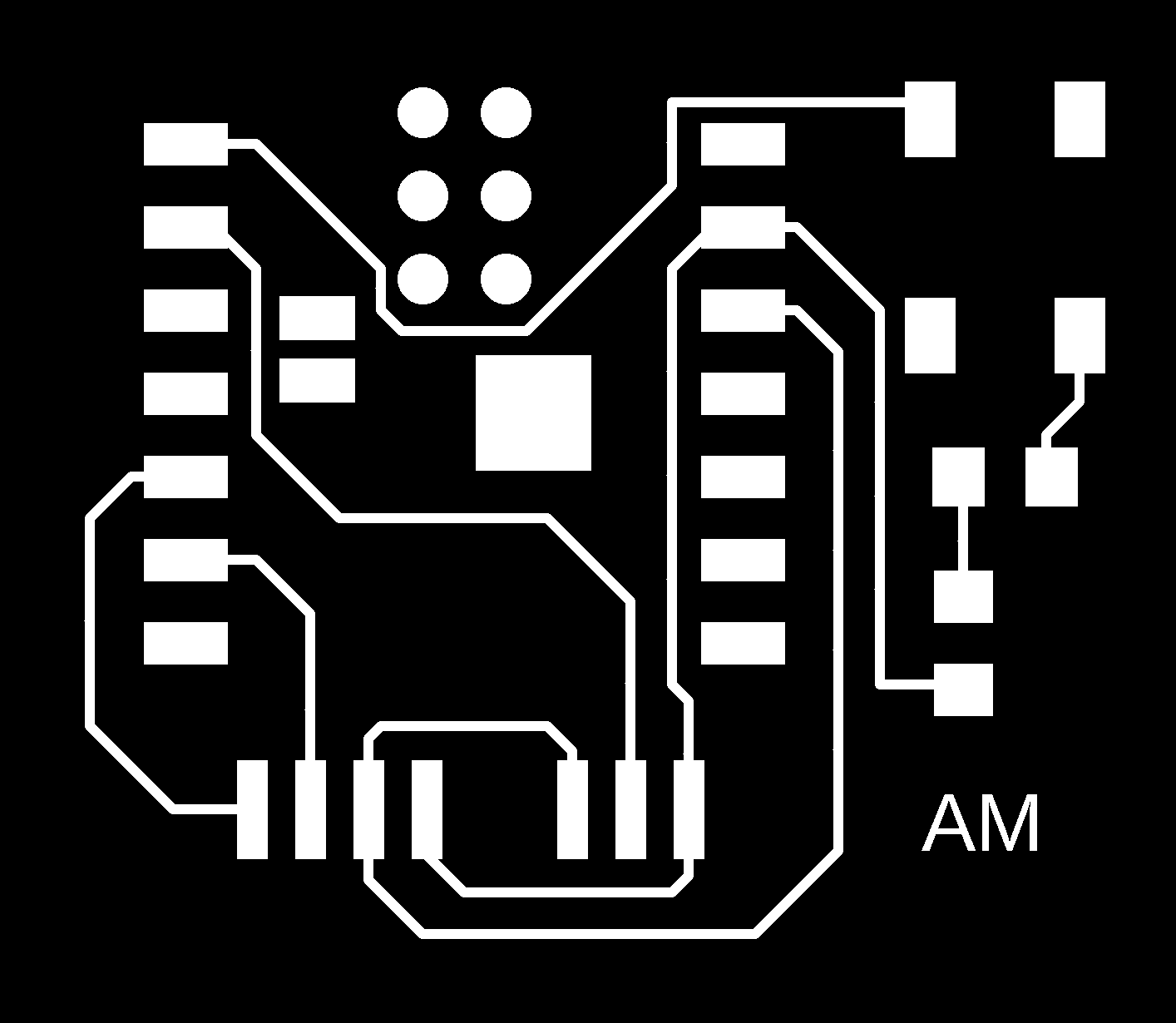
Afterward, I clicked on the Layers tab and selected only the top layer to obtain the traces file in the .png format.
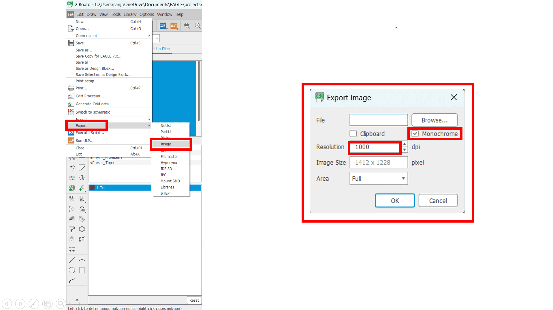
To export the PCB into image format, click on 'Export', then select 'Image'. The Export Image window will appear. Give the file name and locate the file using the browse option. Set the resolution to 1000 dpi and click on the monochrome option. This will make the traces white and the background black. Then select the area as windowed or the full as per our need and click 'OK'. This will generate the .png file of traces.
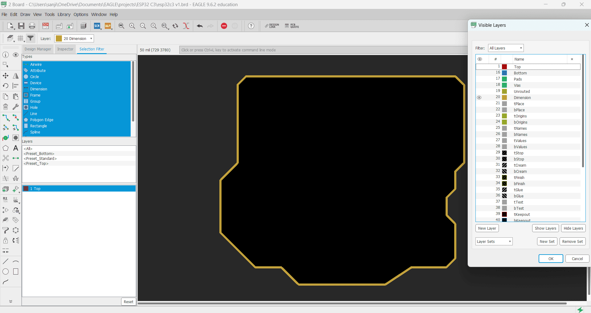
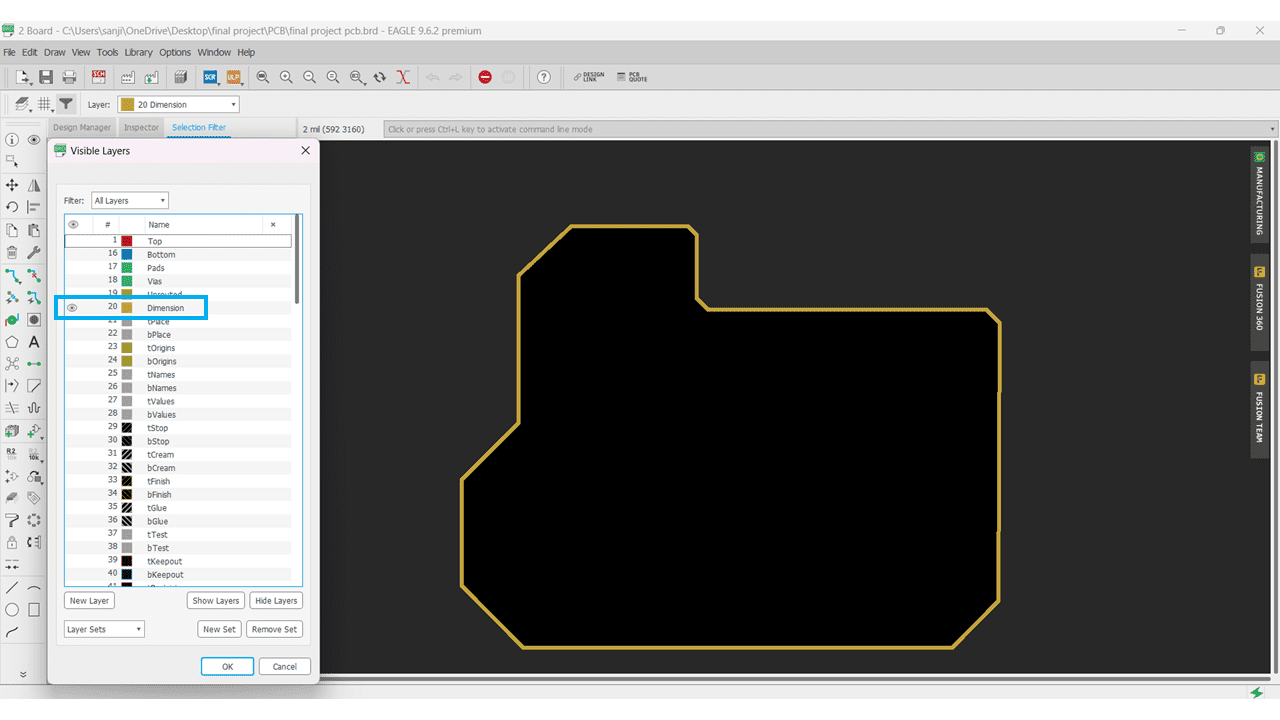
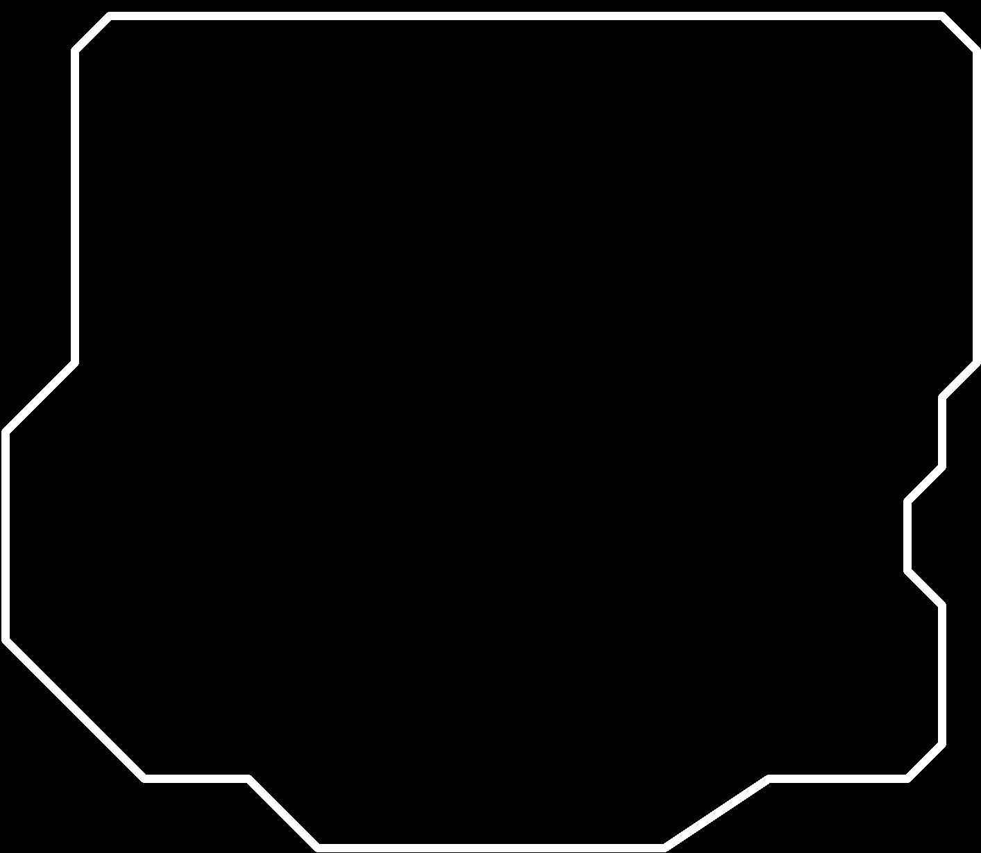
To export the outline of the PCB, follow the same procedure, but select the dimension layer instead of the top layer. in the filter and repeat the above procedure for exporting the image.
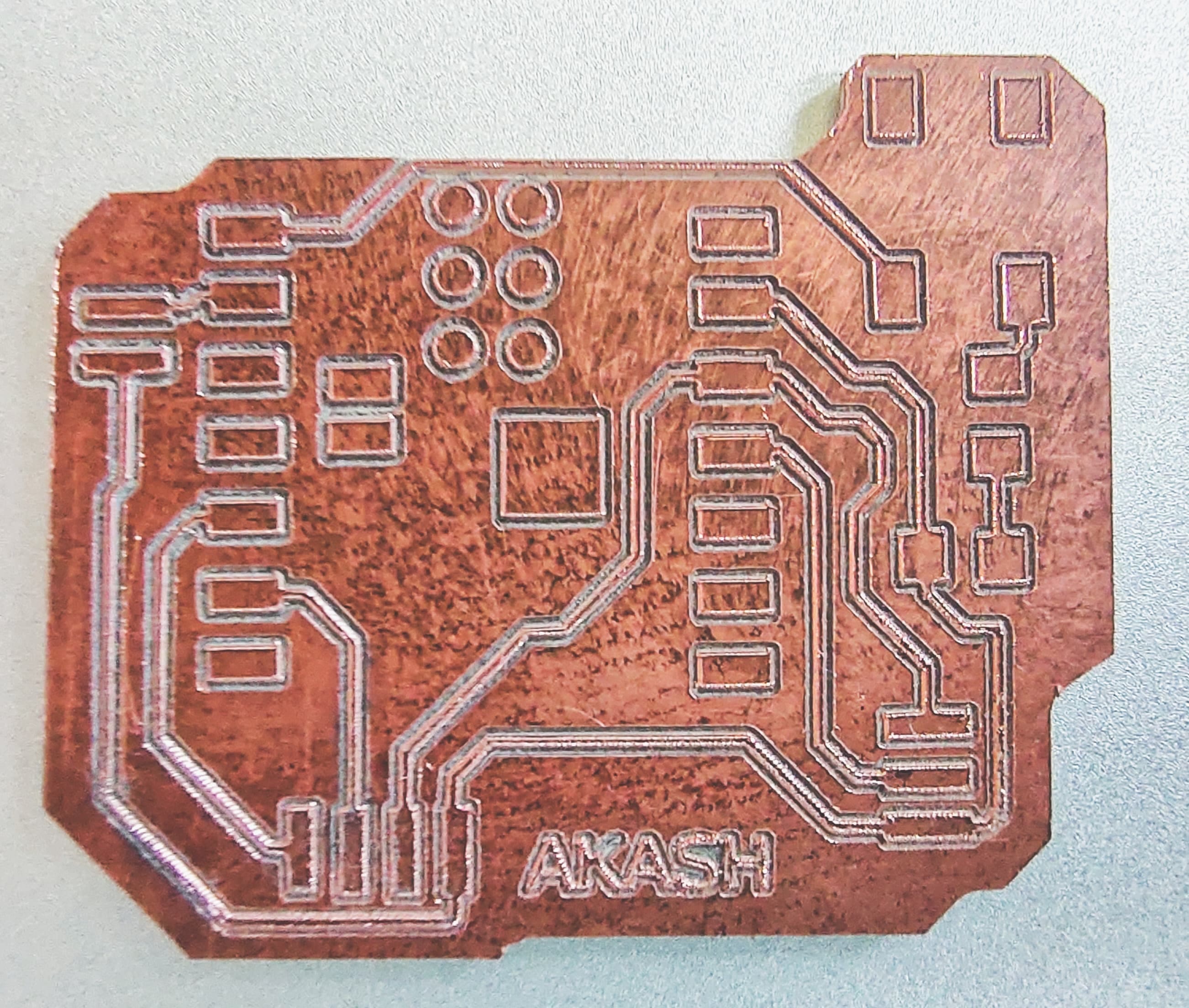
This is the final output I obtained from the PCB design in Eagle software.
I used the Autodesk Eagle Software for PCB Designing.
These are the Components I used while making the schematic of my board.
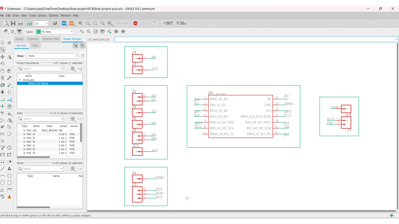
This is the Schematic of my final project board. in which I used 1 pin, 2 pin and 3 pin connectors to connect push buttons and output led.
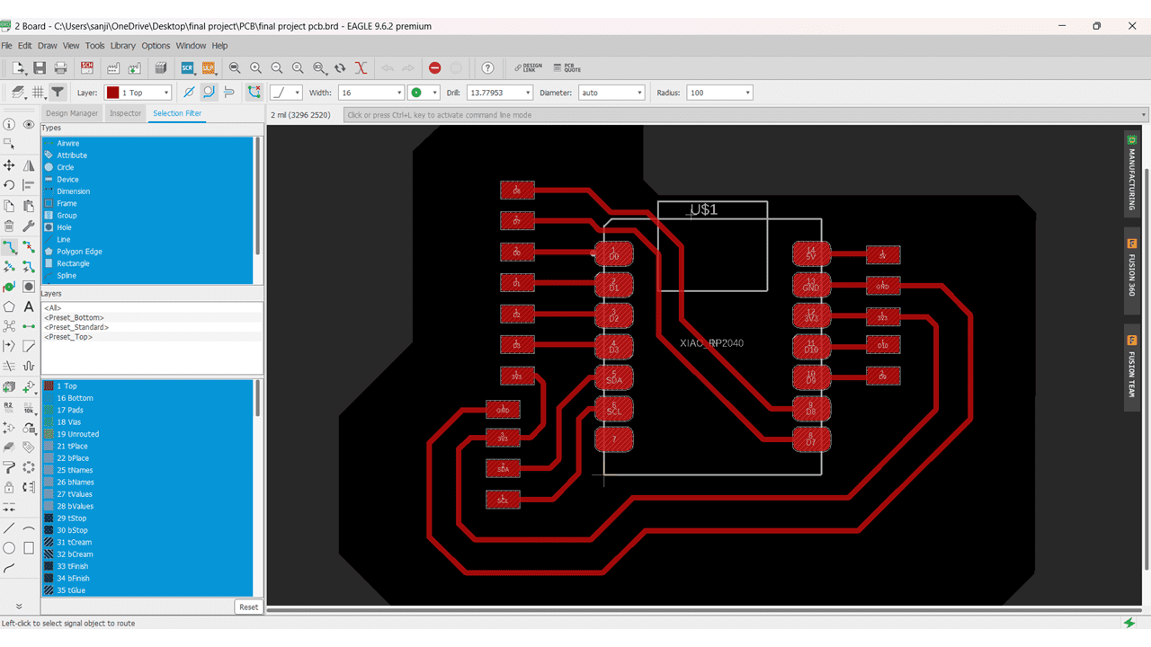
This is the Board that I have designed where trace width is 16 mil.
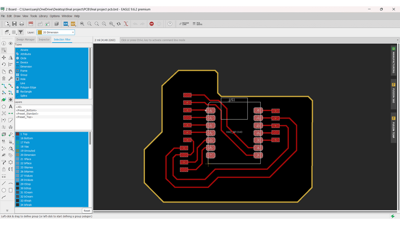
Then I go to Dimension Layer in which I Traced the Outline of the PCB.

For exporting the pcb in .png format I hide all the layers from layer settings except top layer for obtaining the traces.
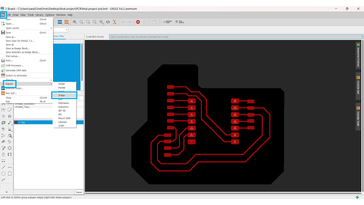
Then Click on File >> Export >> Image option to make it .png file.
here click on monochrome option and set the resolution as 1000 dpi.
do the same procedure for outline of pcb.
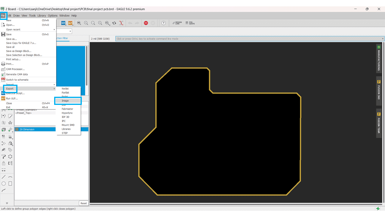
Then Click on File >> Export >> Image option to make it .png file.
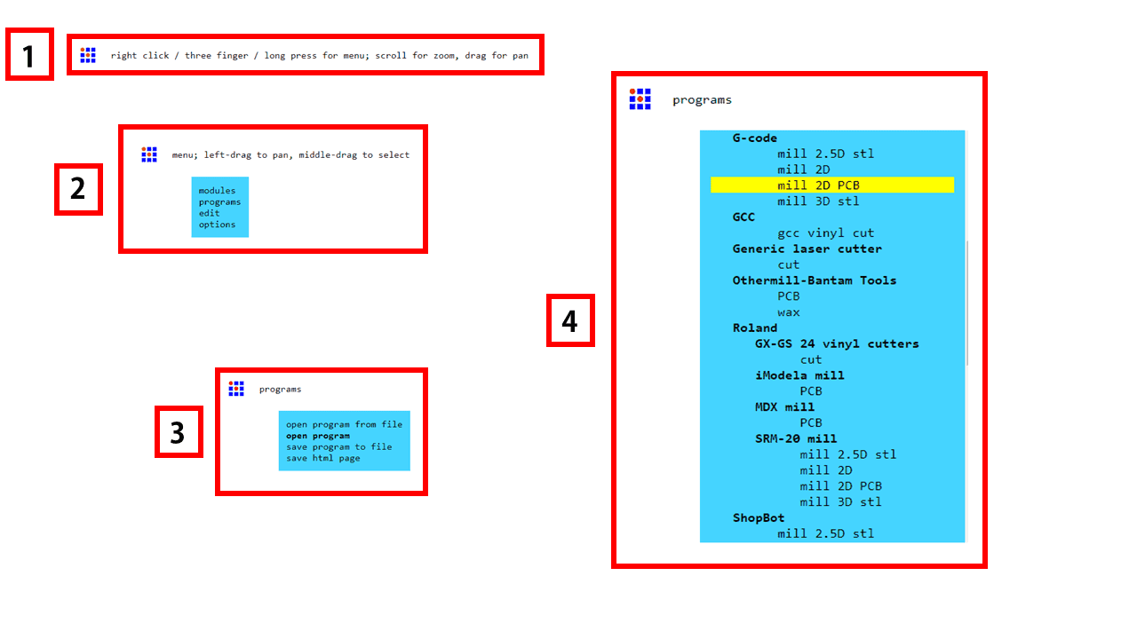
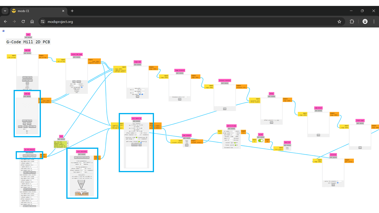
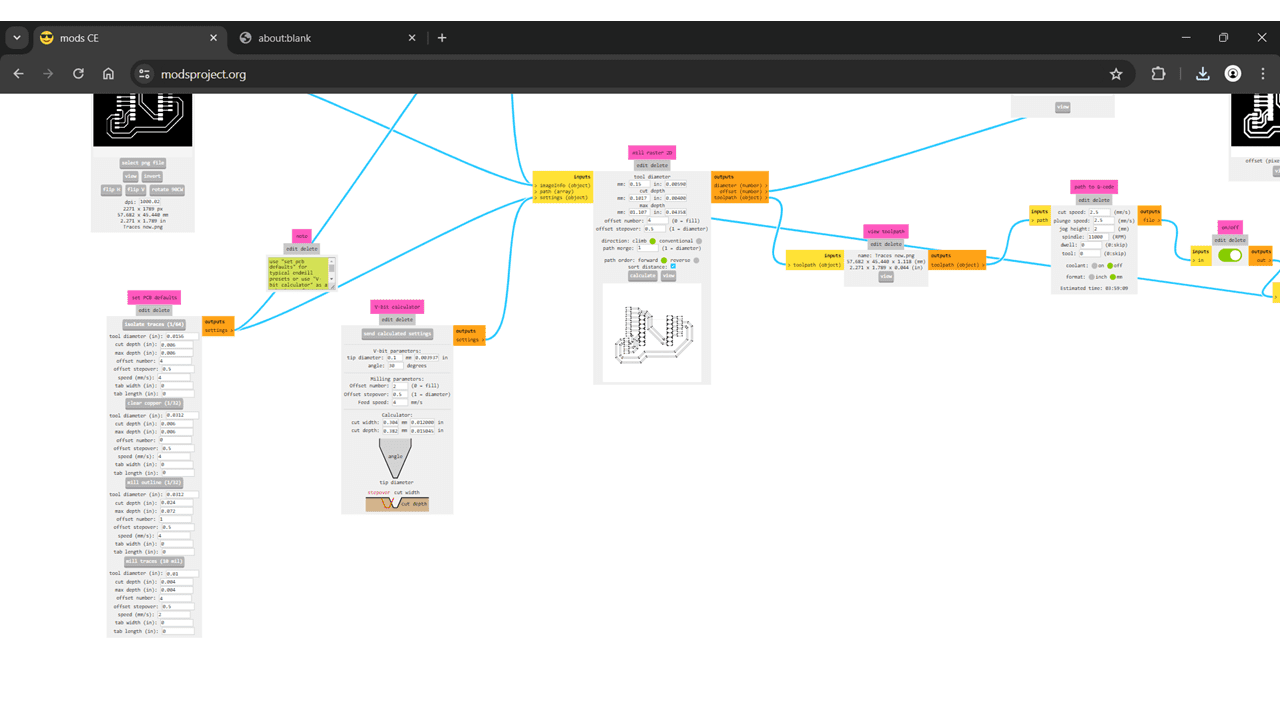
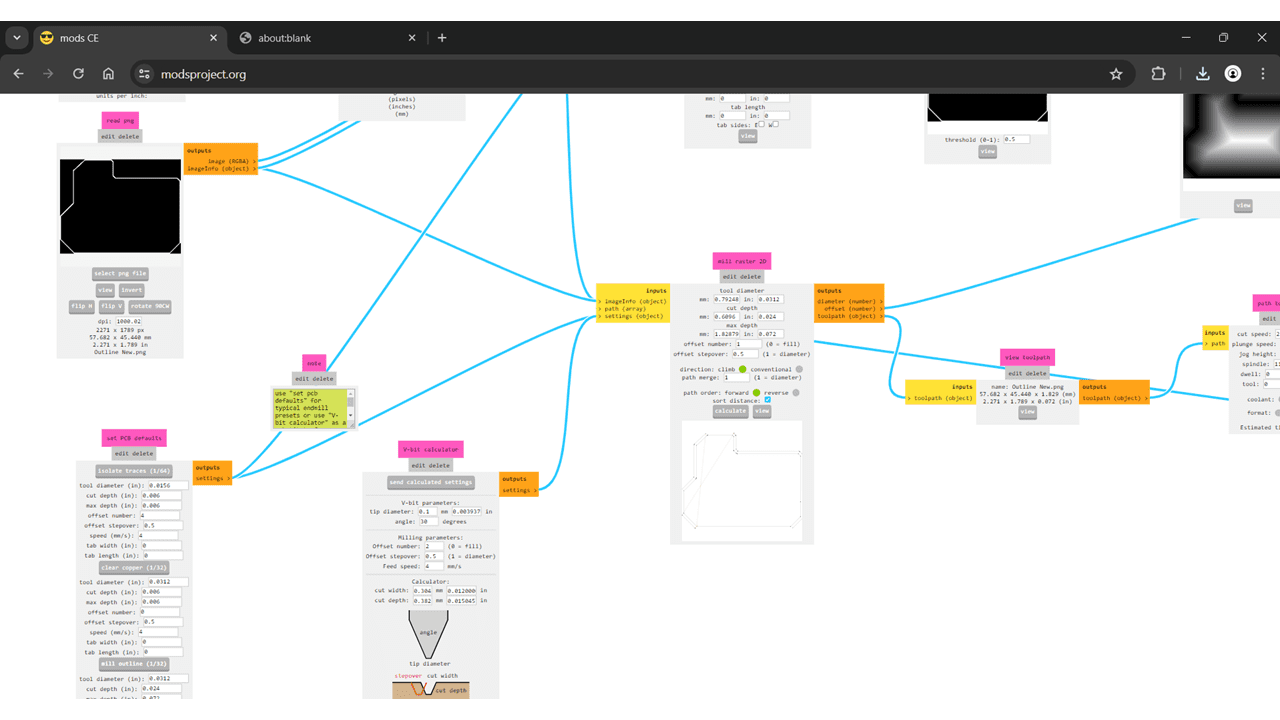
I used the MIT Mods for generating the g code from the .png file that we have exported from the eagle software.
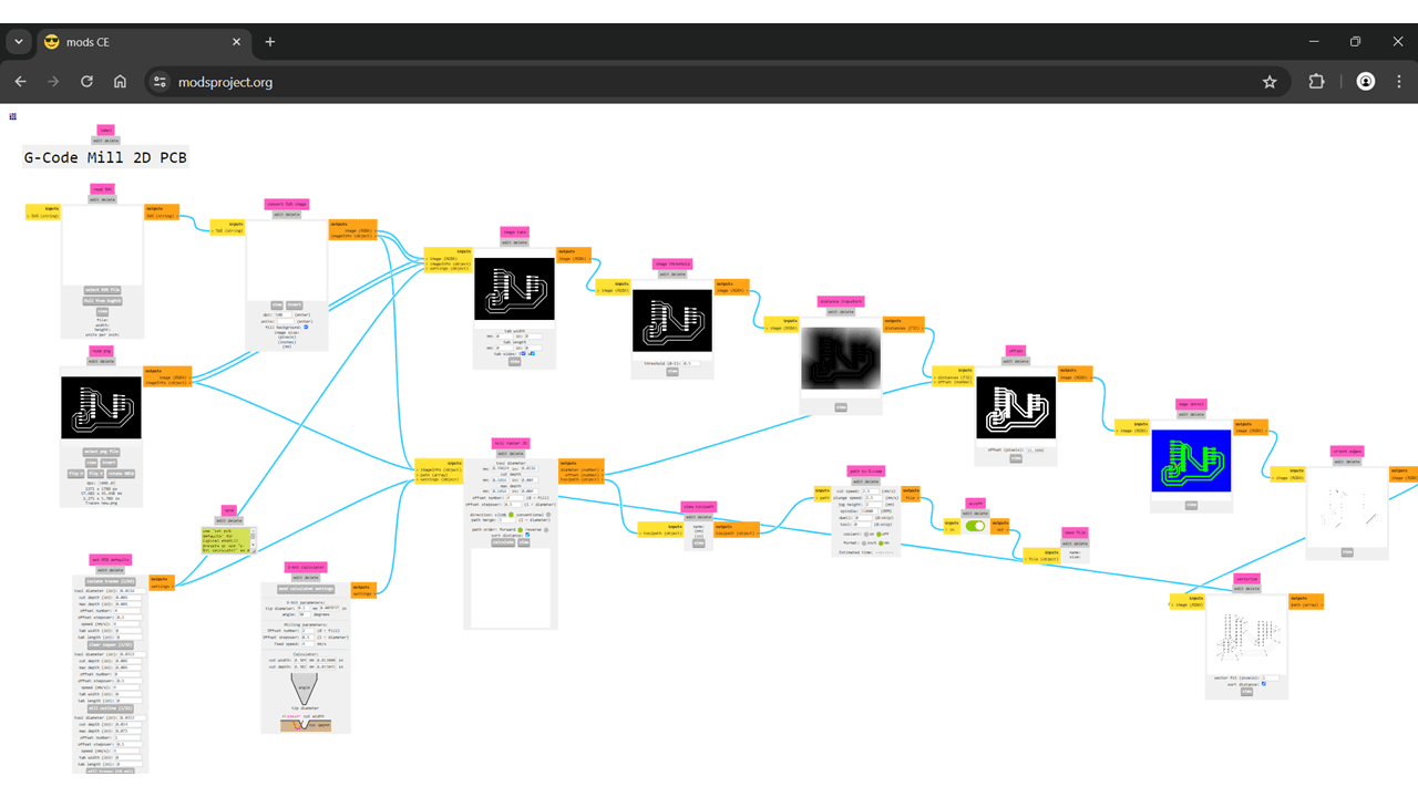
Select the .png file, import it then select Isolate Traces option(1/64). write the tip diameter, cut depth, number of offset tool diameter etc. (Depends on tool), then generate the toolpath by clicking the generate button then the .nc file will be downloaded, open thet file into notepad and change the file extension as .gcd for our machine.
Parameters:
Tip Diameter - 0.1mm
Tool Diameter - 0.15mm
Cut Depth - 0.1016mm
Offset - 4
For Outline select mill outline (1/32) then tool diameter as 1mm and the cut depth 1.8mm, nuumber of passes 3. then generate the toolpath by clicking the generate button then the .nc file will be downloaded, open thet file into notepad and change the file extension as .gcd for our machine.
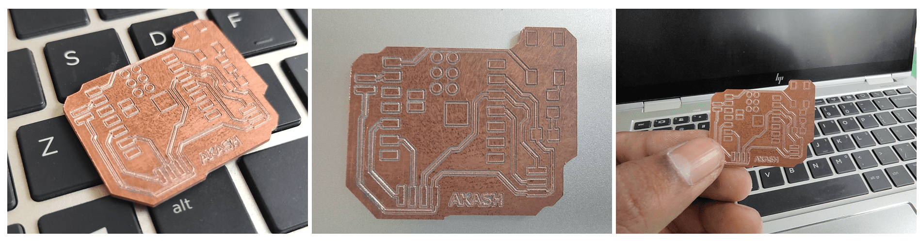
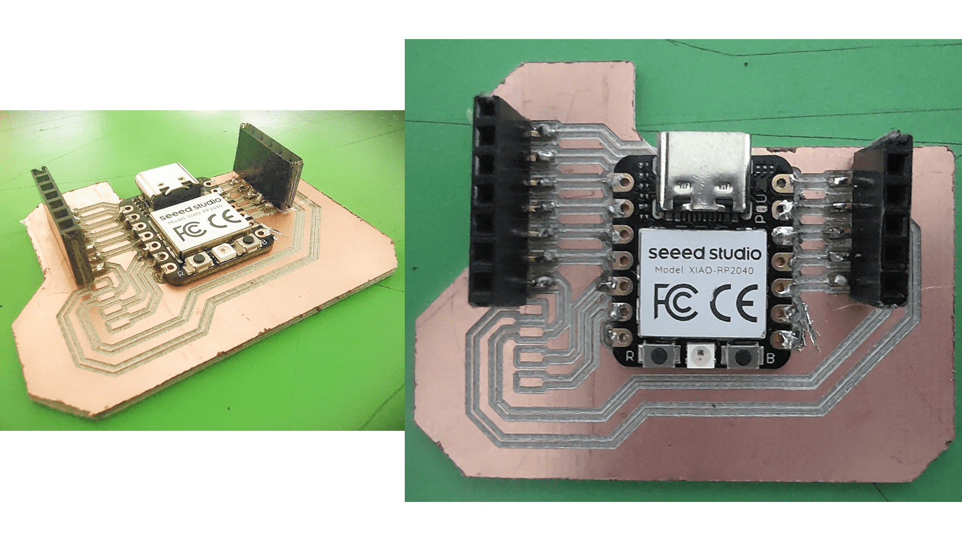
This is the final output I got after pcb milling and soldering.
Code:
        #define button1 D0

        #define button2 D1

        #define button3 D2

        #define button4 D3

        #define led D10


        #define input1 D7

        #define input2 D8

        int mode = 0;


        bool state1;

        bool state2;

        bool state3;

        bool state4;


        bool input1_state ;

        bool input2_state ;


        void setup() {

          pinMode(led,OUTPUT);

          pinMode(button1,INPUT_PULLDOWN);

          pinMode(button2,INPUT_PULLDOWN);

          pinMode(button3,INPUT_PULLDOWN);

          pinMode(button4,INPUT_PULLDOWN);

          pinMode(input1,INPUT_PULLDOWN);

          pinMode(input2,INPUT_PULLDOWN);

          Serial.begin(9600);

        }


        void loop() {


        state1 = digitalRead(button1);

        state2 = digitalRead(button2);

        state3 = digitalRead(button3);

        state4 = digitalRead(button4);

        input1_state = digitalRead(input1);

        input2_state = digitalRead(input2);

          if(state1 == HIGH)

          {

            mode = 1;

            Serial.println("mode1");

          } else if ( state3 == HIGH)

          {

            mode = 3;

            Serial.println("mode3");

          } else if ( state2 == HIGH)

          {

            Serial.println("mode2");

            mode = 2;

          } else if ( state4 == HIGH)

          {

            Serial.println("mode4");

            mode = 4;

          }

        Serial.println(mode);

        switch(mode) {

          case(1):

          digitalWrite(led,(input1_state && input2_state));

          Serial.println("and");

          break;

          case(2):

          digitalWrite(led,(input1_state || input2_state));

          Serial.println("or");

          break;

          case(3):

          digitalWrite(led,!(input1_state && input2_state));

          Serial.println("nand");

          break;

          case(4):

          digitalWrite(led,!(input1_state || input2_state));

          Serial.println("nor");

          break;

          default :

          Serial.println("press input buttons");

          break;

          Serial.println(mode);

        }


        }
Traces.
Interior.
Arduino Code.