For more information about the idea click here.
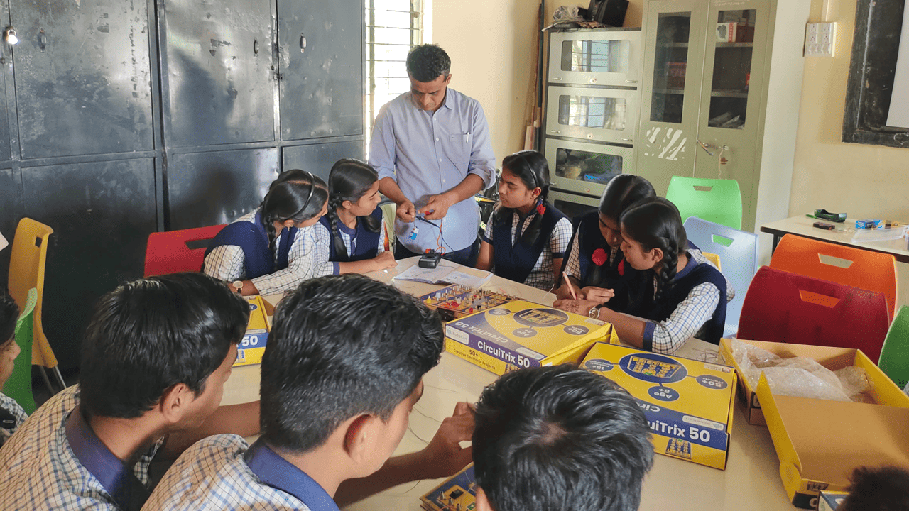
As a mechatronics engineering student, I organize an electronics learning session at the Sanjivani Academy for 9 to 14-year-old students. During the session, I noticed that the students faced many difficulties. From this experience, I got the idea of creating an electronics learning kit.
I got this idea of creating a kit for schools in rural areas. We conduct sessions on electronics for 9-year-old students, where my instructor and I provide easy-to-understand knowledge about electronics. During these sessions, we use a kit provided by the government or an organization to the school. Then, I thought, why can't we produce our own electronics kit at a cheaper cost and make it more engaging?
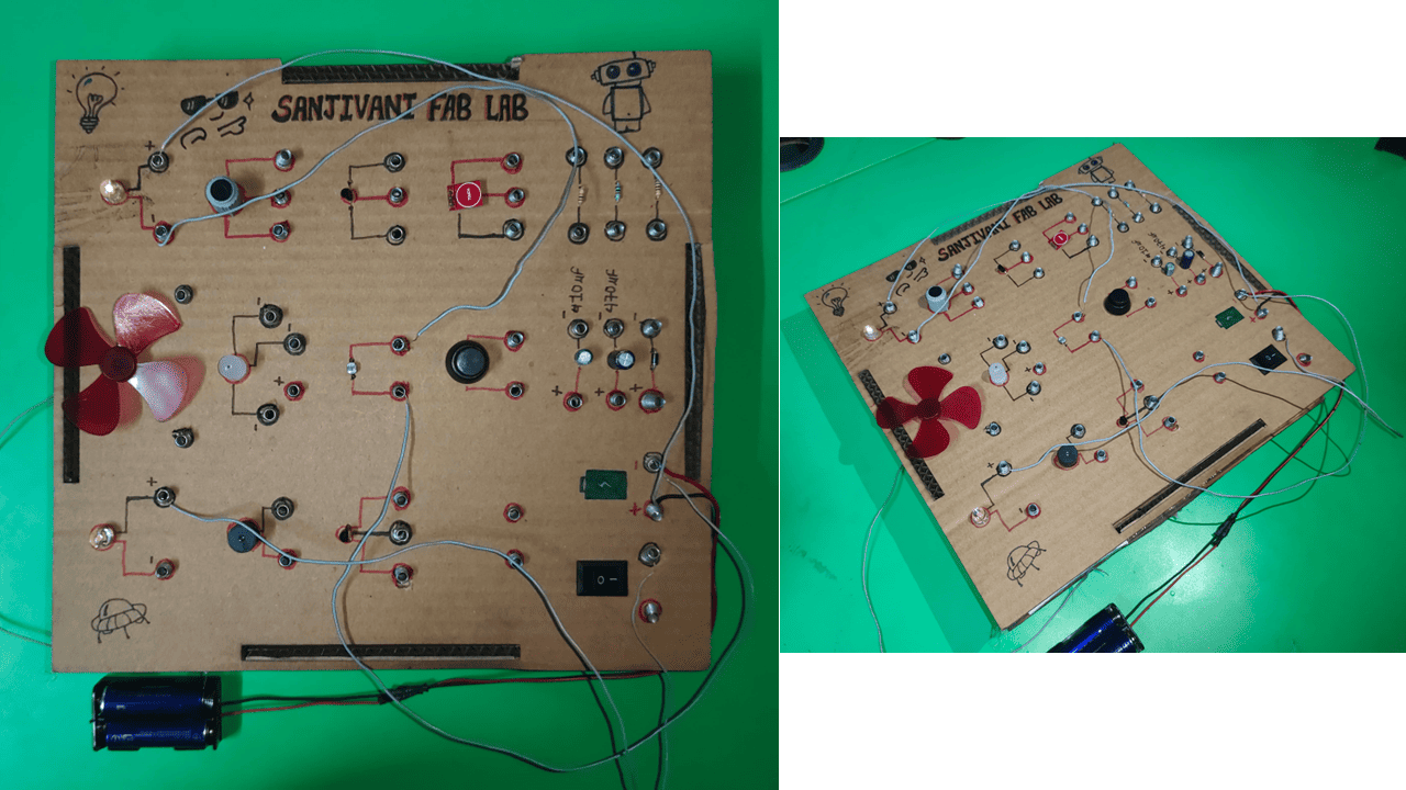
This is the kit we currently use for teaching students at the school. Then, I began to contemplate changing and improving its design and electronics to make it easier and more interesting for the students.
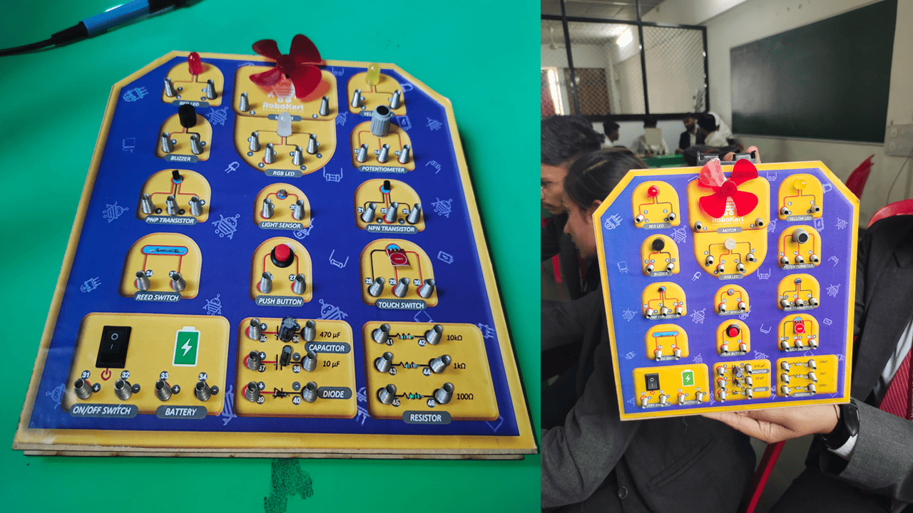
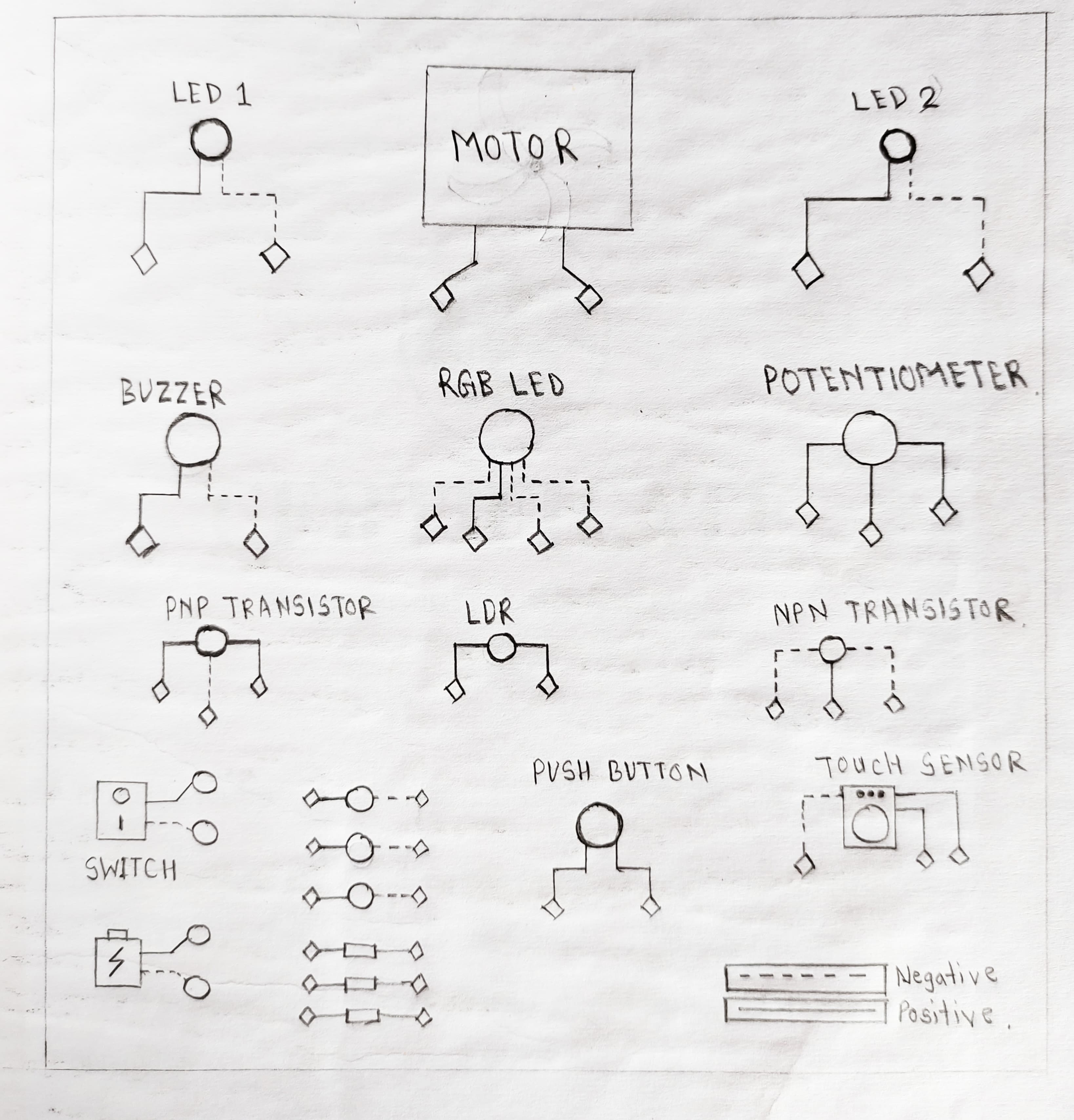
This is the first version of my project, where I utilized laser cutting to create the cardboard frame. Then, I incorporated connectors, motors, LEDs, RGB, PNP and NPN transistors, potentiometer, switch, battery, LDRs, and touch sensor.
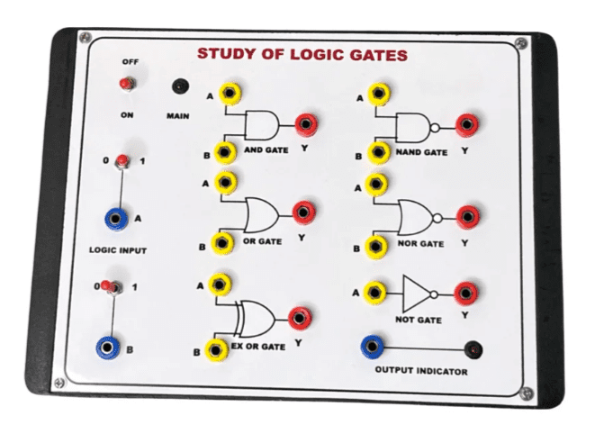
Additionally, I am planning to include logic gates in the kit, as shown in the image below.
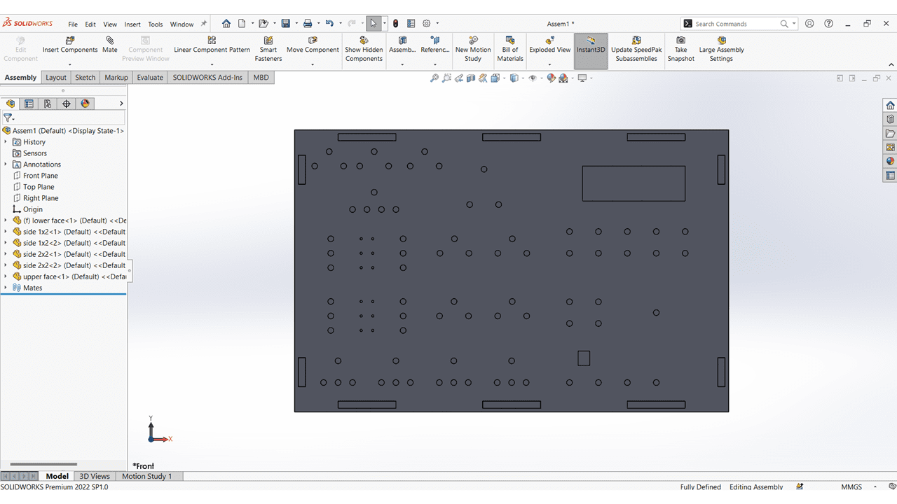
This is the upper and the lower faces of my electronics learning kit.
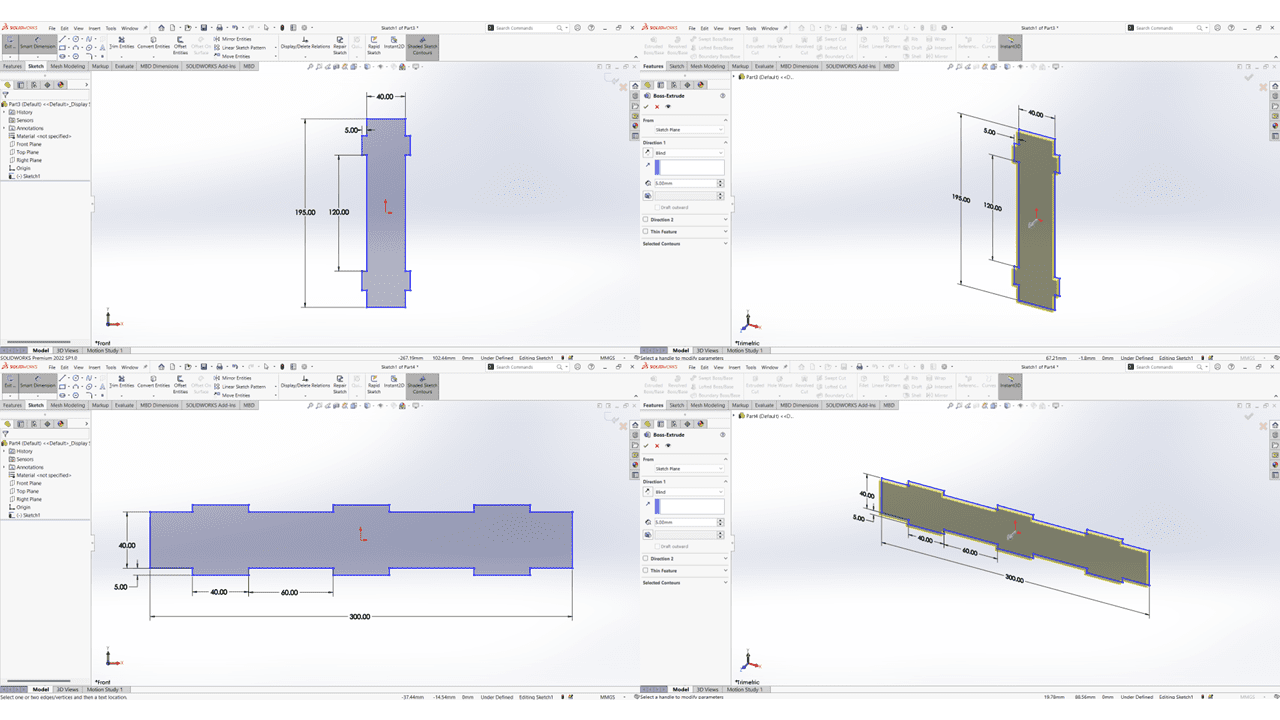
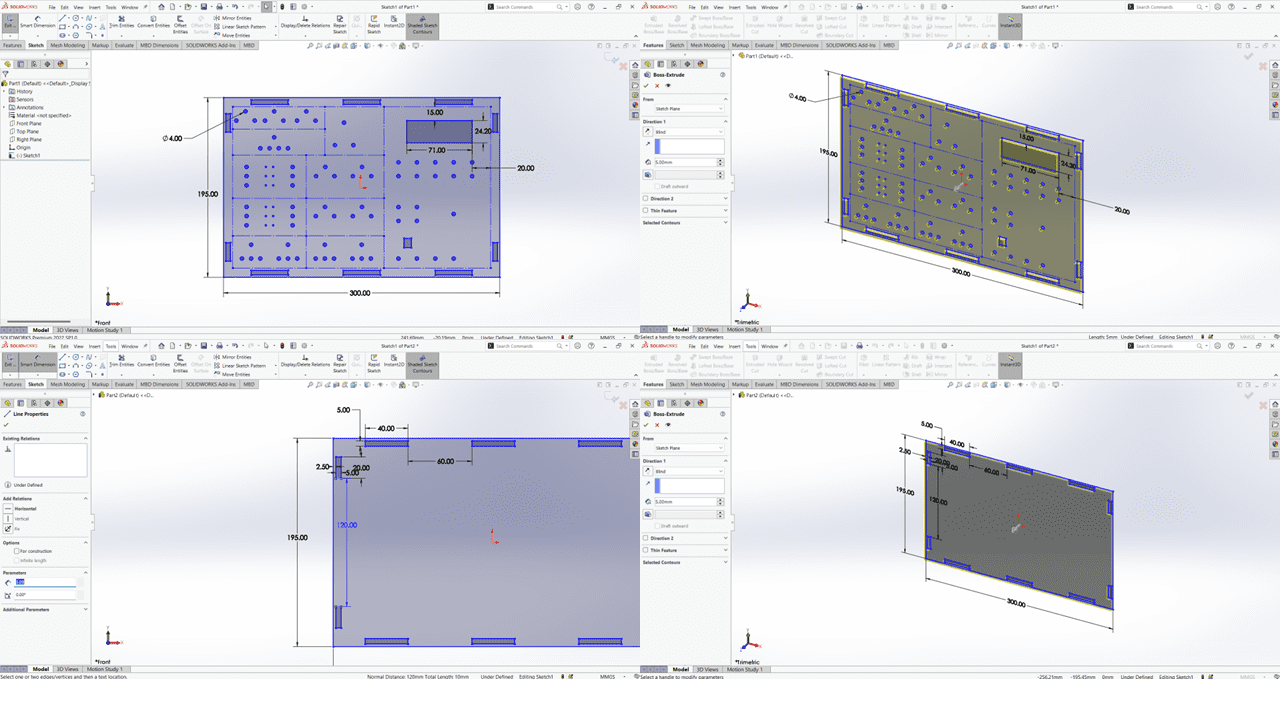
This is the Vertical and Horizontal sides having the thickness of 5mm each.
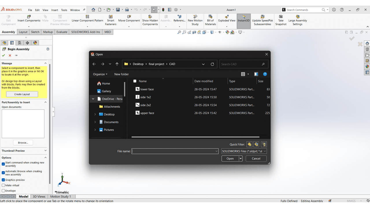
After that used the Solidworks Assembly option for making the Assembly of all the Parts.
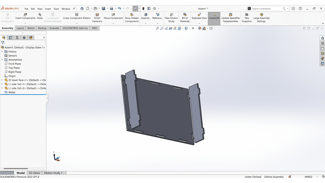
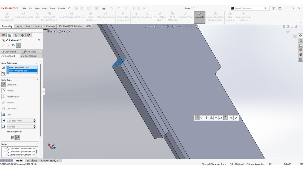
I mate all the Vertical Faces with Lower Face.
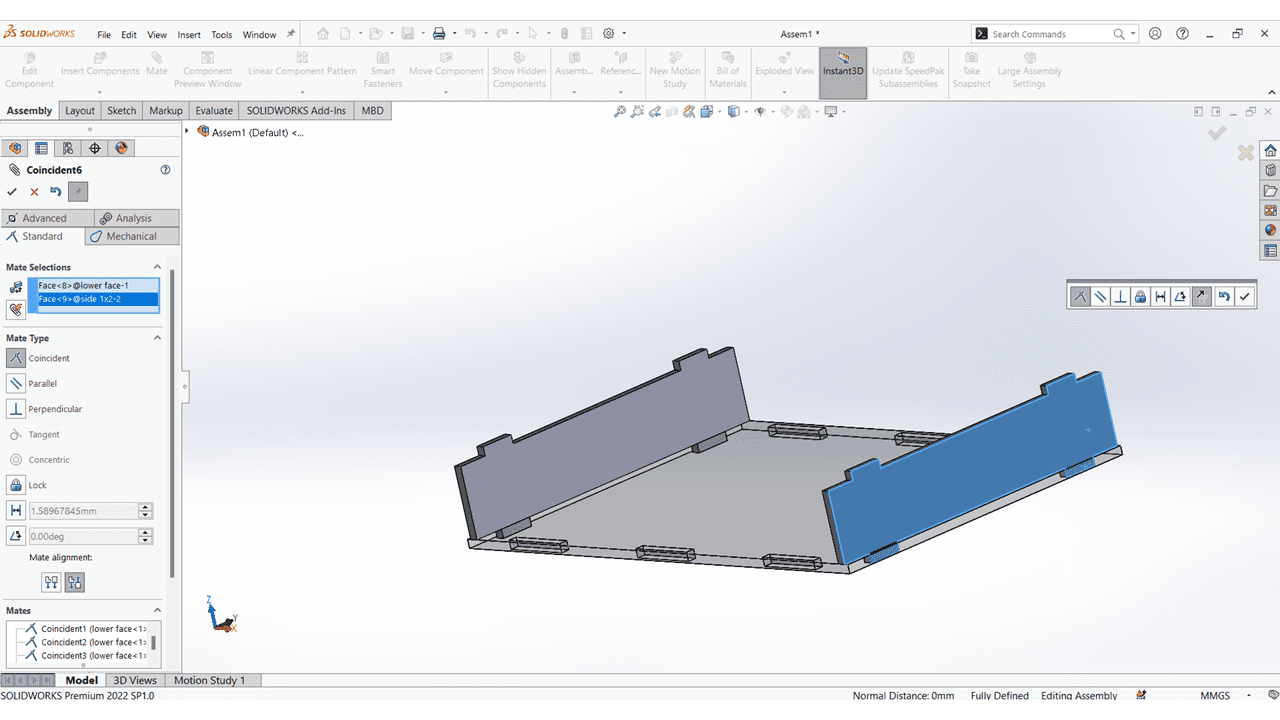
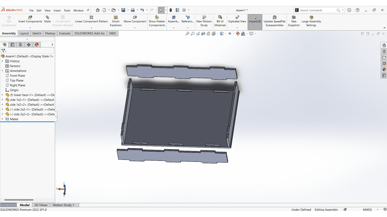
I mate the Horizontal Faces with Lower Face.
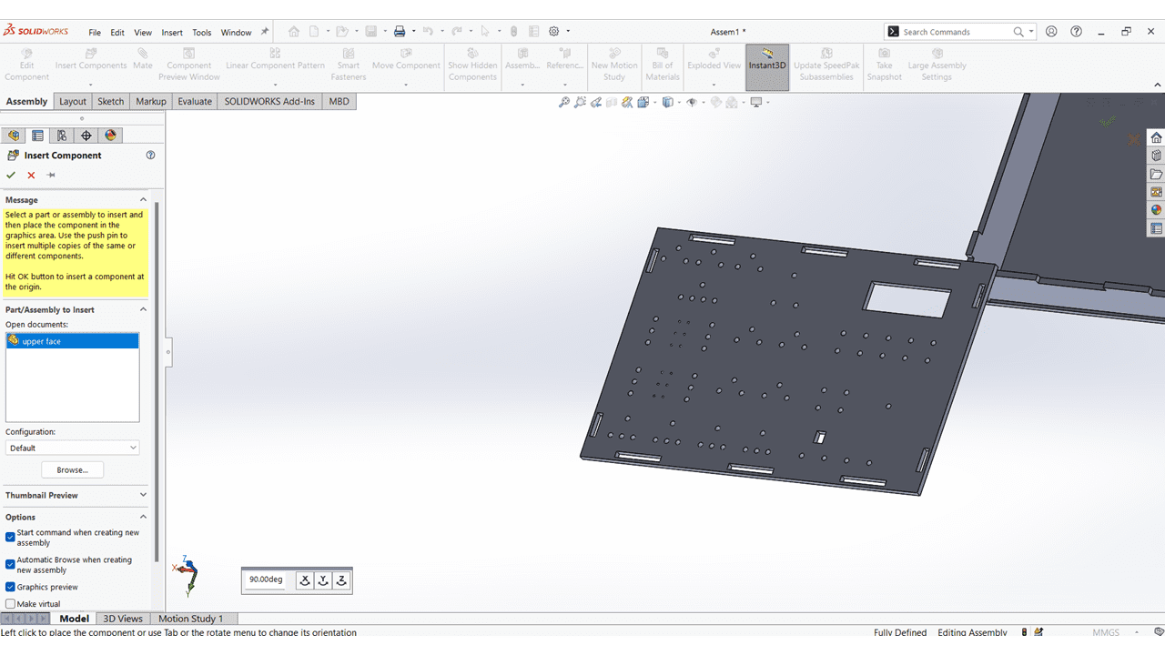
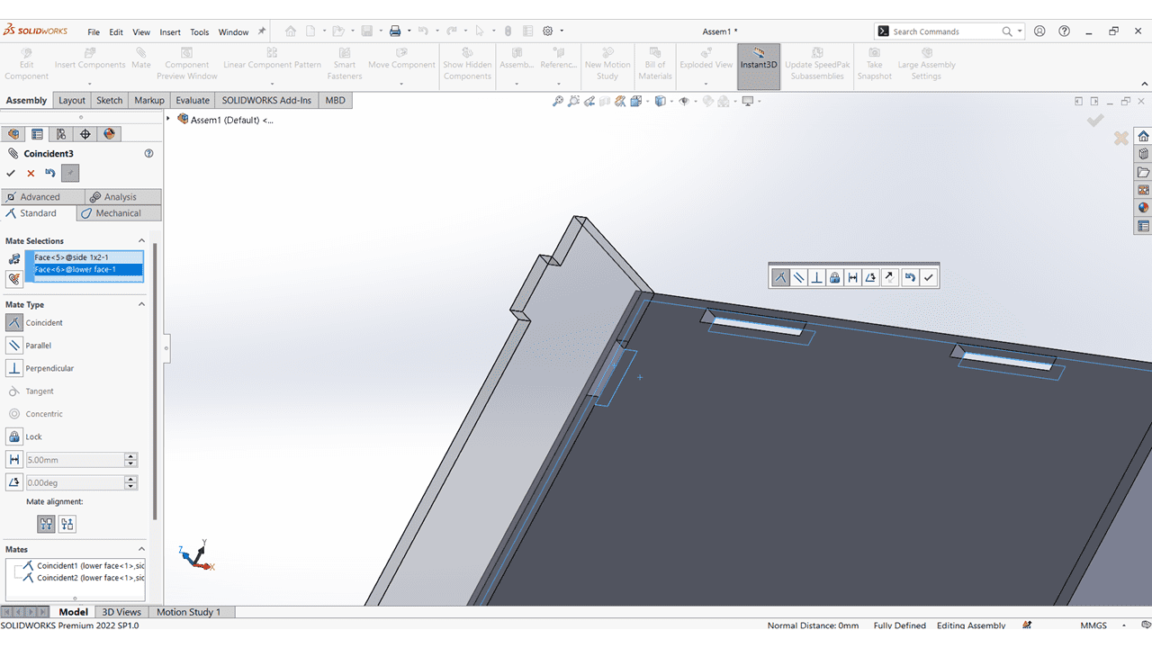
I added upper face of the kit and mate it with the slots.
This is the TOP view of my Elctronics Learning kit.
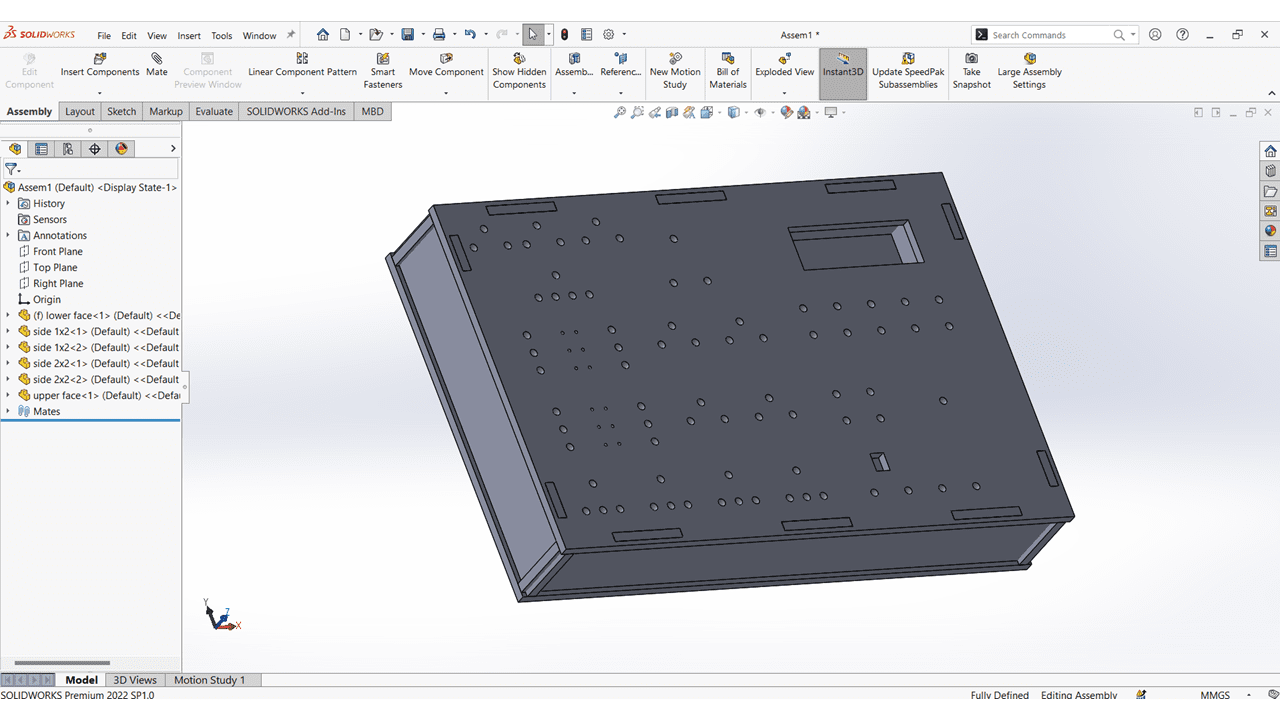
Isometric view of my project
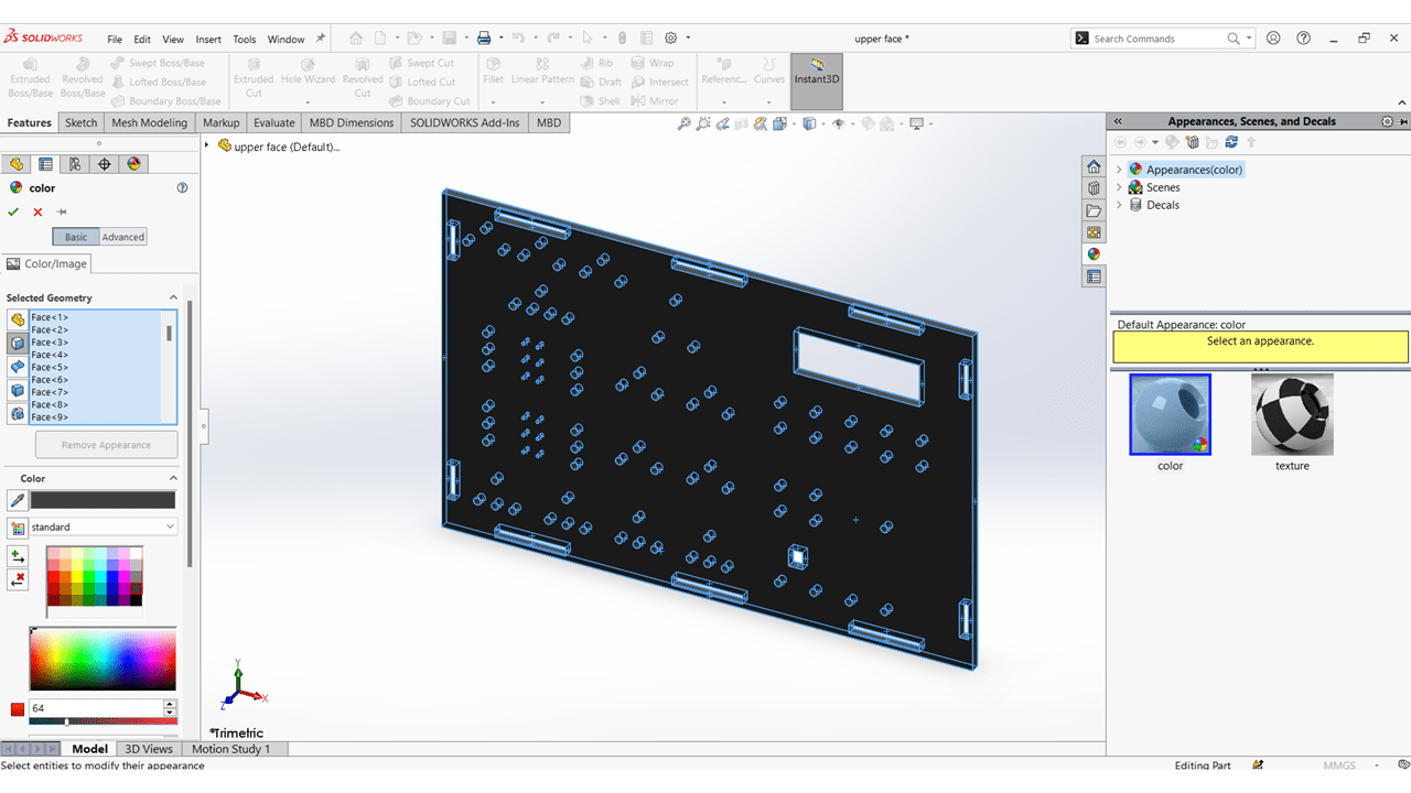
I coloured all the parts.
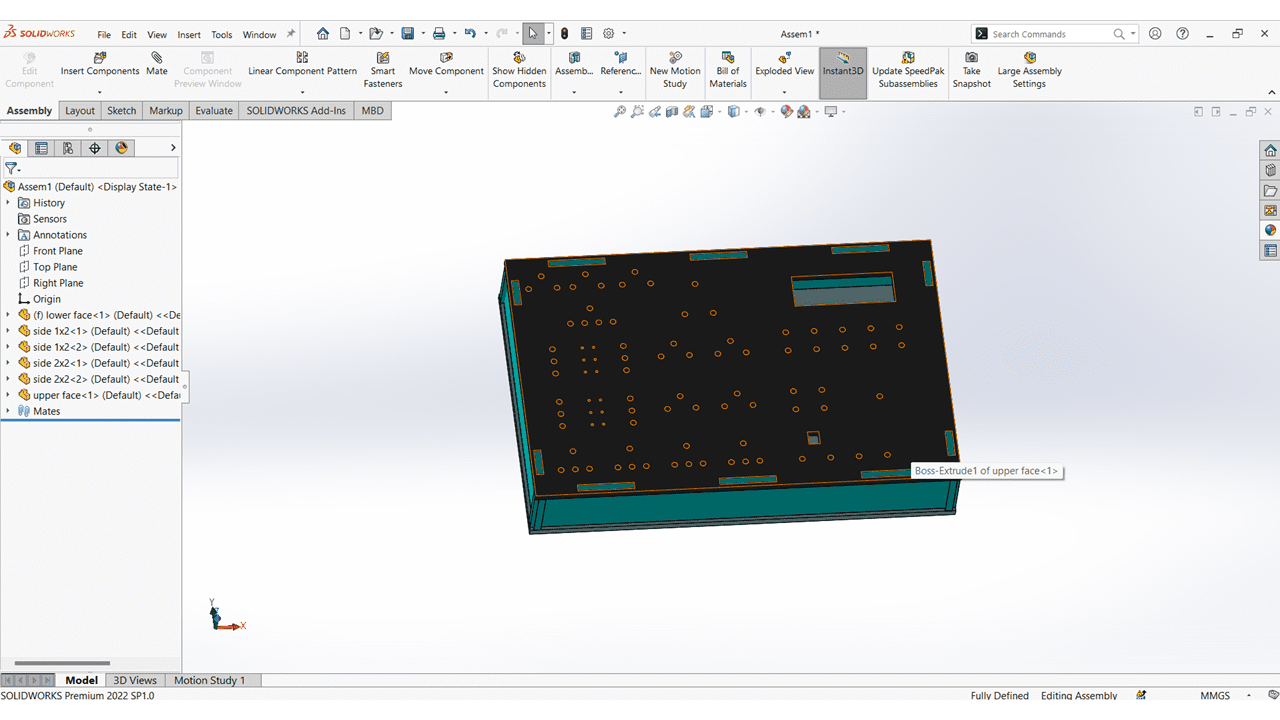
This is the Casing of my Electronics Learning kit.
I used the Autodesk Eagle Software for PCB Designing.
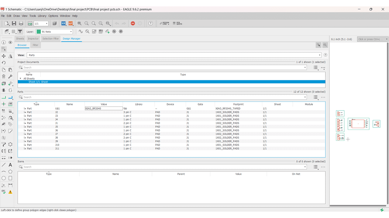
These are the Components I used while making the schematic of my board.
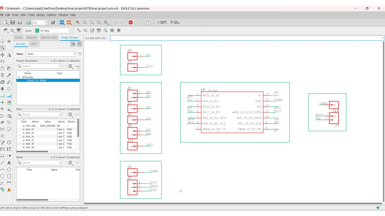
This is the Schematic of my final project board. in which I used 1 pin, 2 pin and 3 pin connectors to connect push buttons and output led.
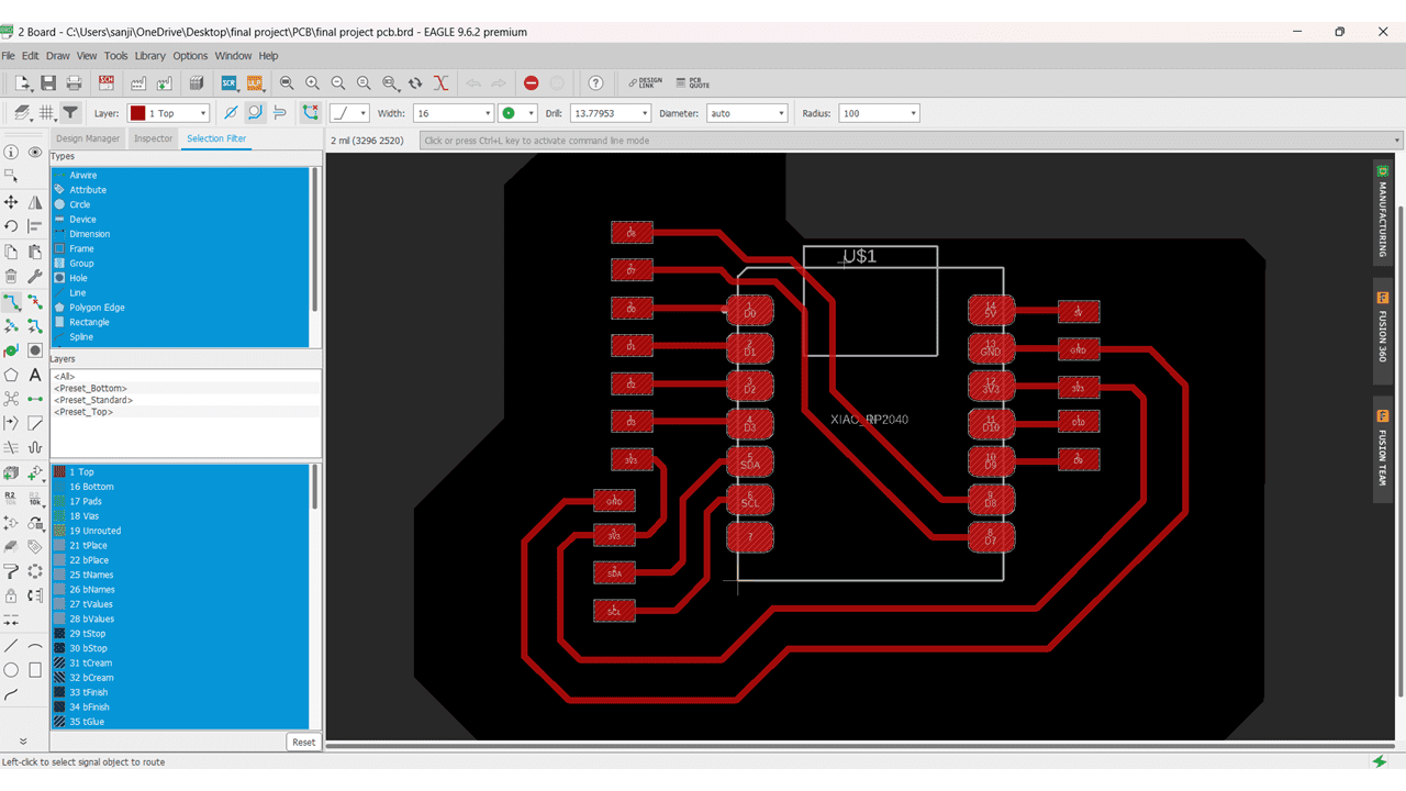
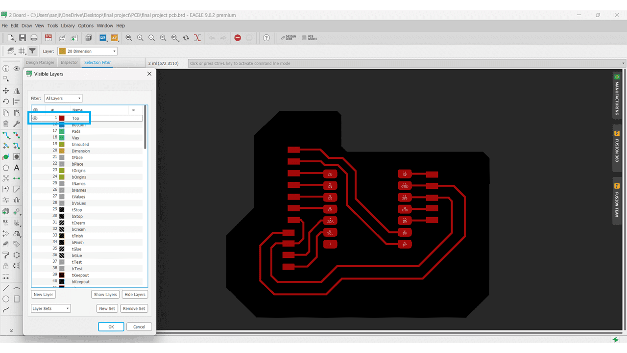
This is the Board that I have designed where trace width is 16 mil.
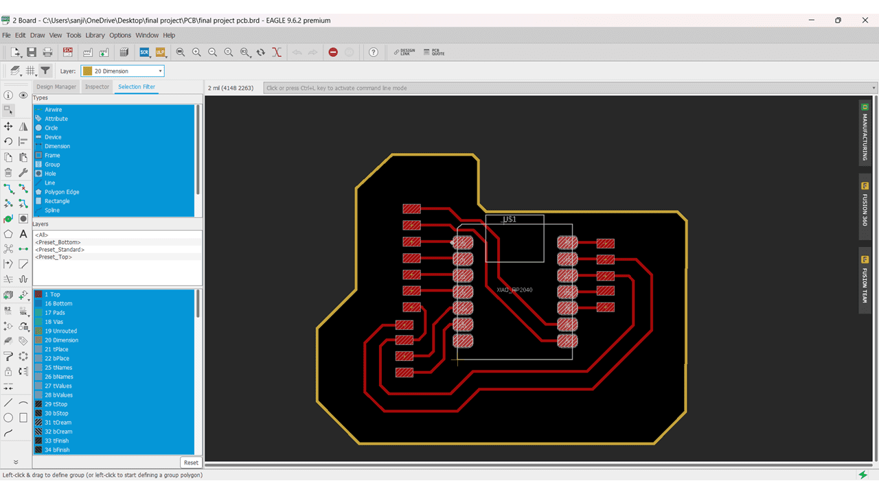
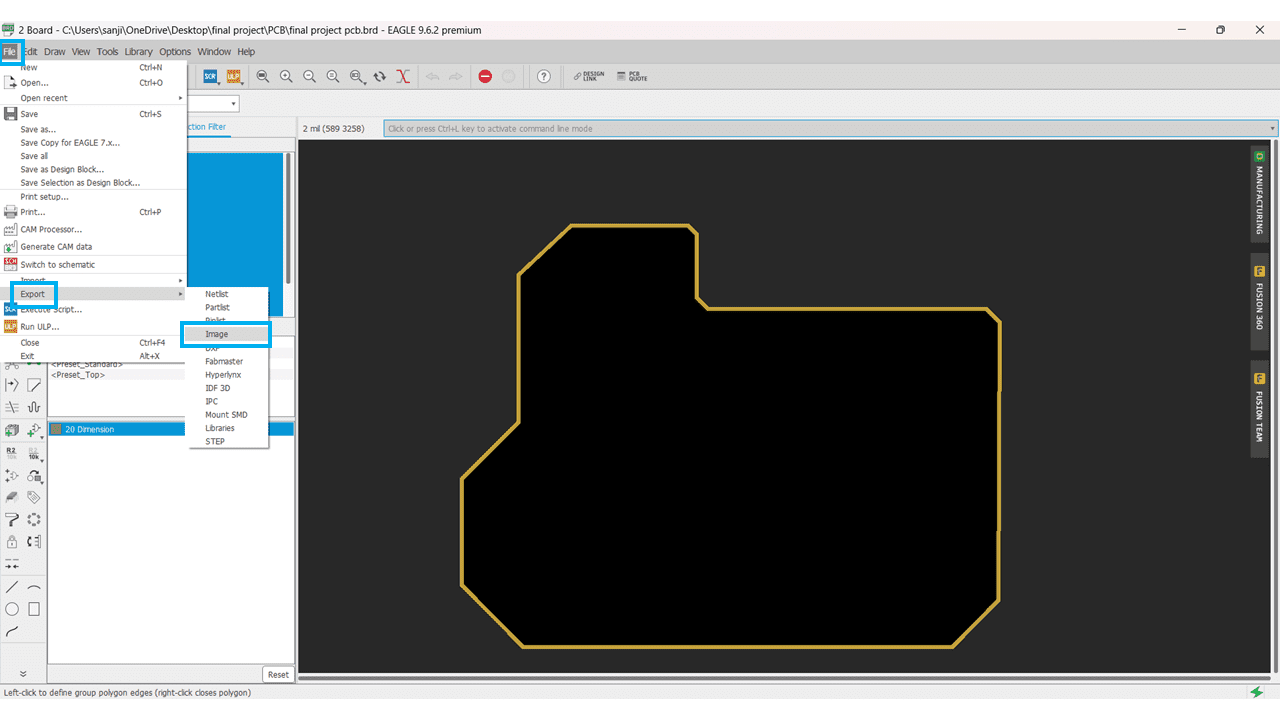
Then I go to Dimension Layer in which I Traced the Outline of the PCB.

For exporting the pcb in .png format I hide all the layers from layer settings except top layer for obtaining the traces.
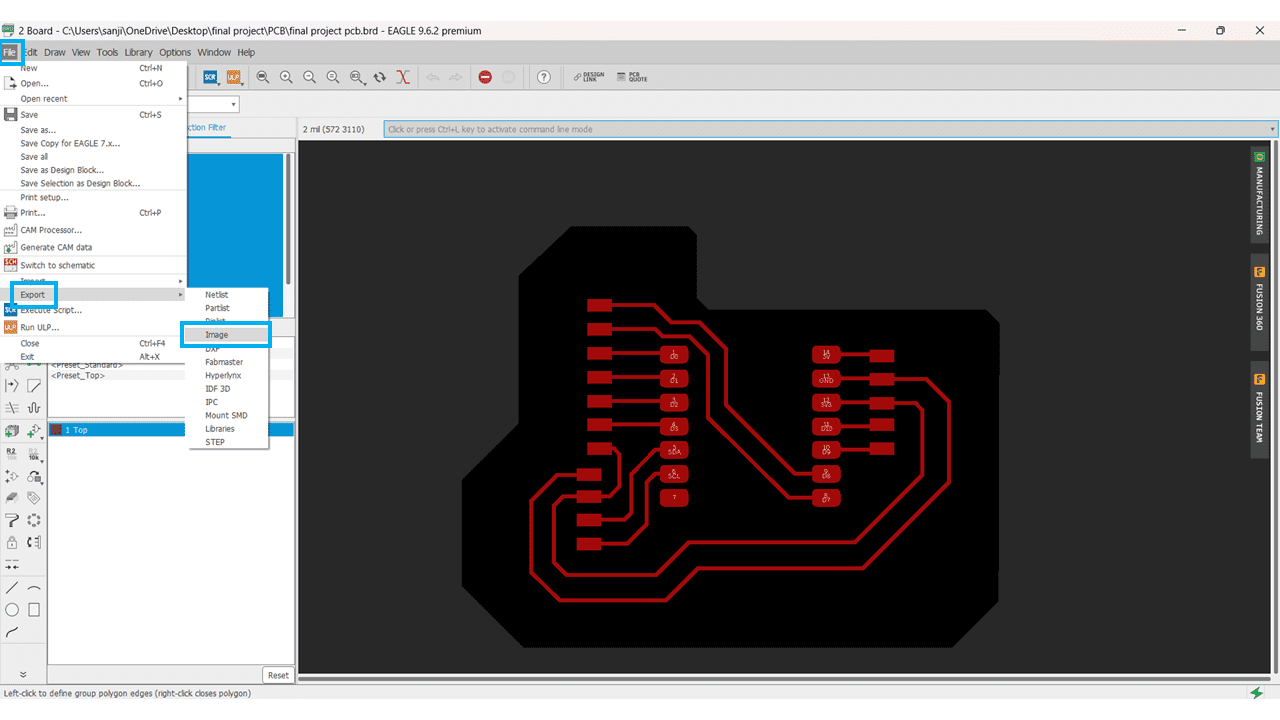
Then Click on File >> Export >> Image option to make it .png file.
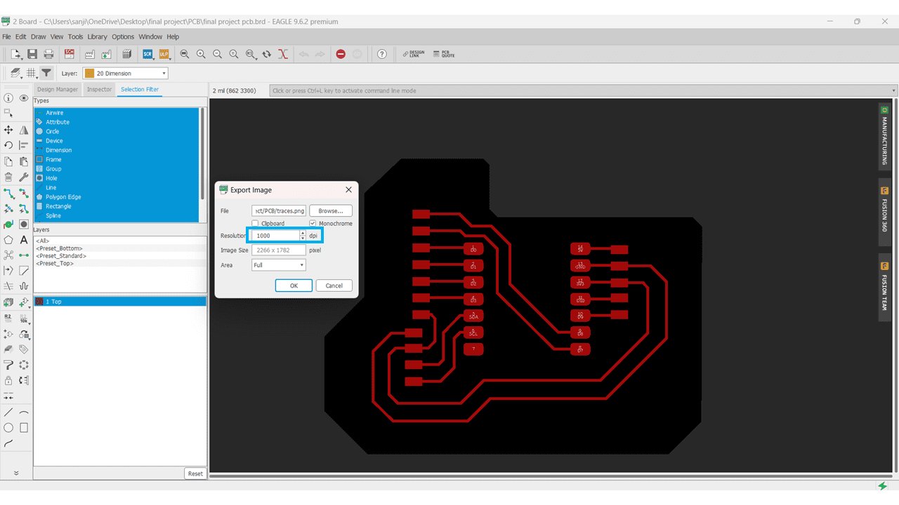
here click on monochrome option and set the resolution as 1000 dpi.
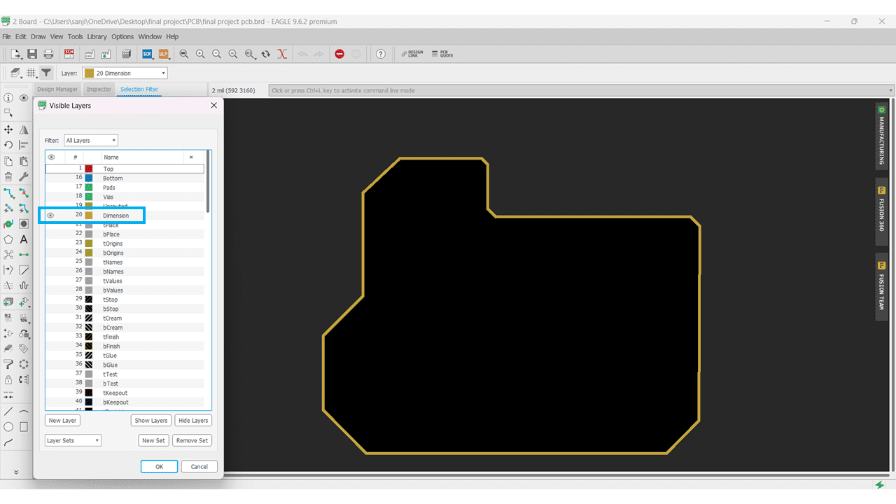
do the same procedure for outline of pcb.
Then Click on File >> Export >> Image option to make it .png file.
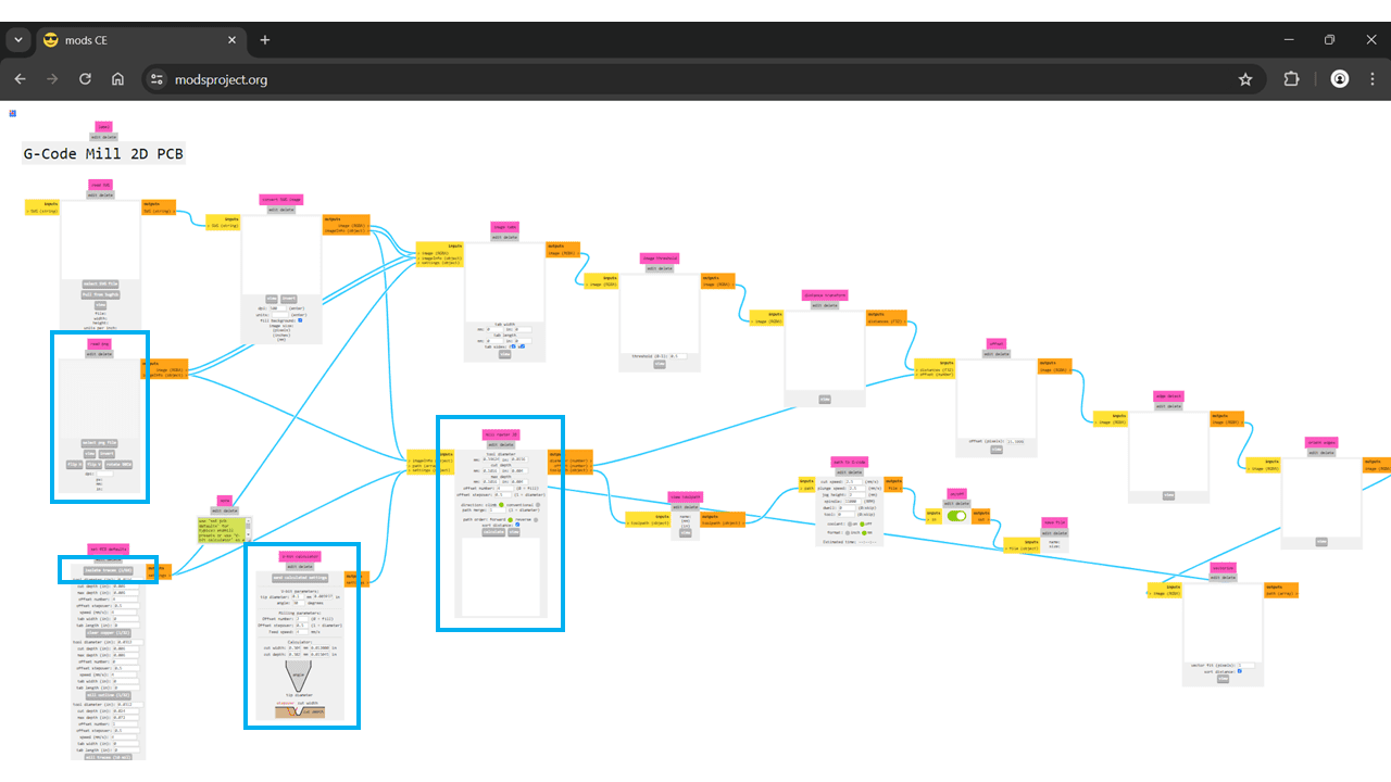
I used the MIT Mods for generating the g code from the .png file that we have exported from the eagle software.
Select the .png file, import it then select Isolate Traces option(1/64). write the tip diameter, cut depth, number of offset tool diameter etc. (Depends on tool), then generate the toolpath by clicking the generate button then the .nc file will be downloaded, open thet file into notepad and change the file extension as .gcd for our machine.
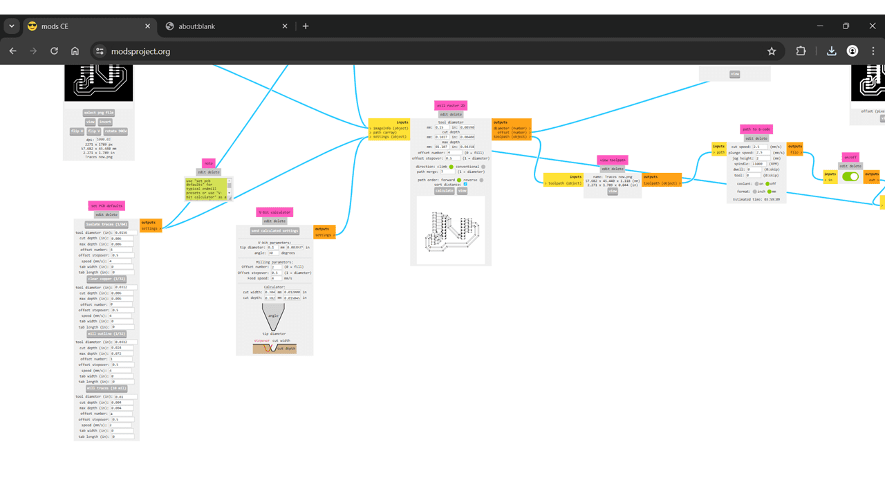
Parameters:
Tip Diameter - 0.1mm
Tool Diameter - 0.15mm
Cut Depth - 0.1016mm
Offset - 4
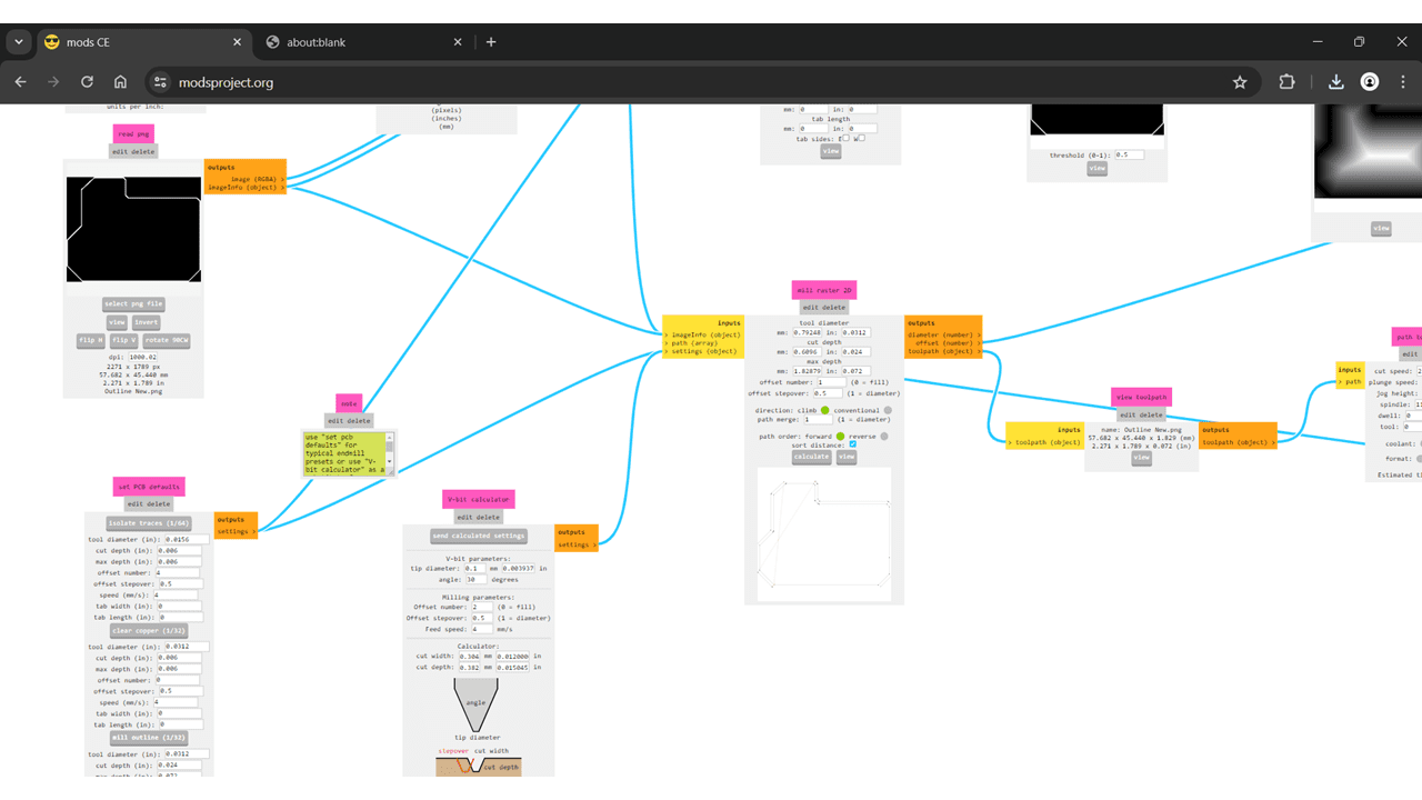
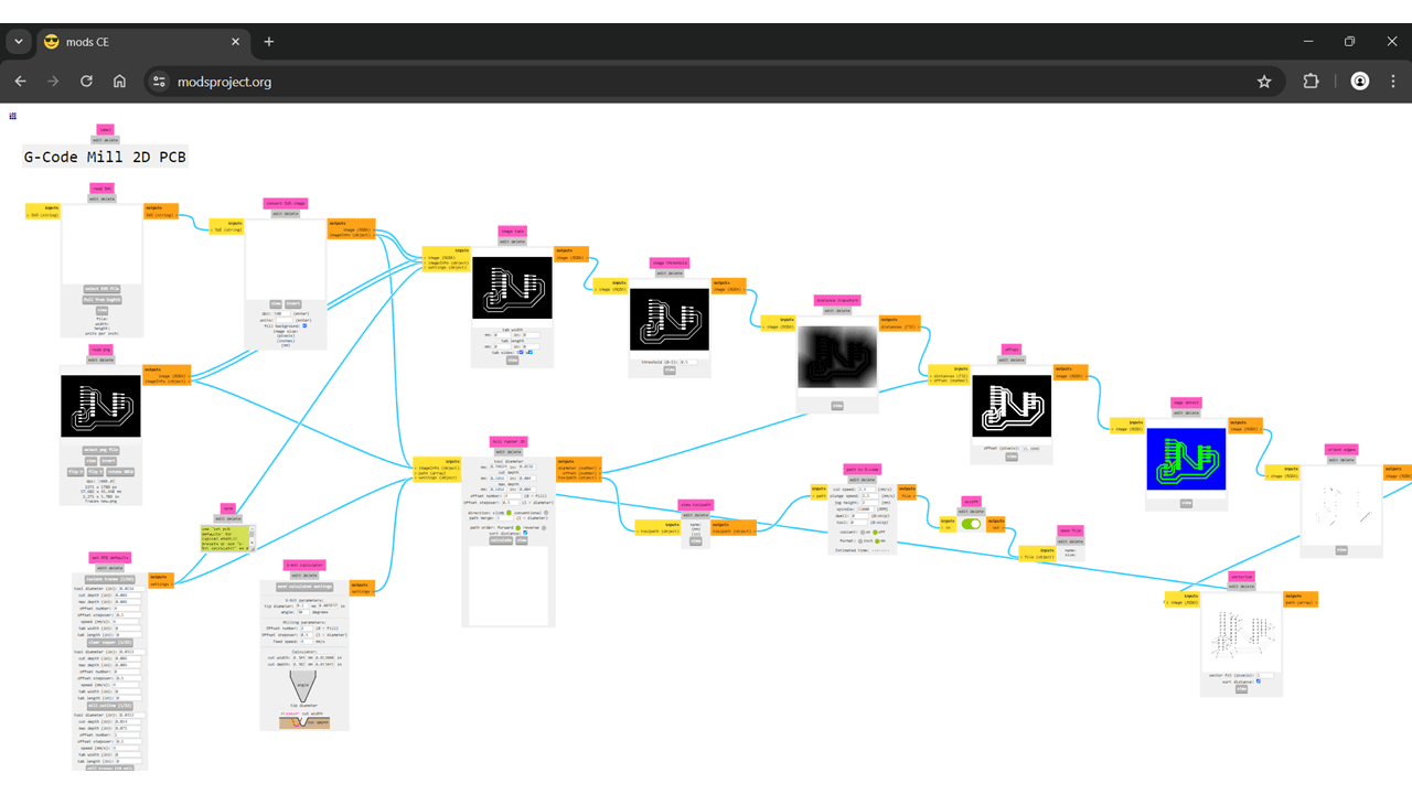
For Outline select mill outline (1/32) then tool diameter as 1mm and the cut depth 1.8mm, nuumber of passes 3. then generate the toolpath by clicking the generate button then the .nc file will be downloaded, open thet file into notepad and change the file extension as .gcd for our machine.
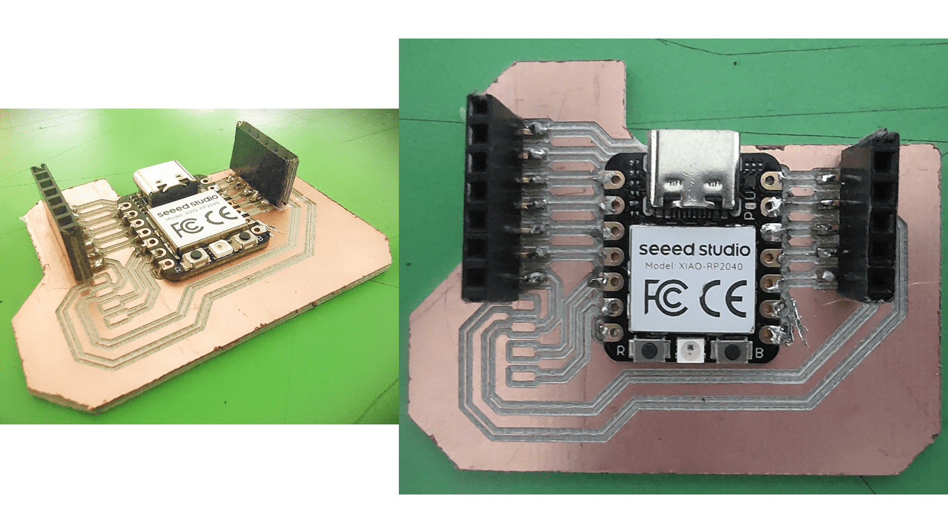
This is the final output I got after pcb milling and soldering.
Code:
        #define button1 D0

        #define button2 D1

        #define button3 D2

        #define button4 D3

        #define led D10


        #define input1 D7

        #define input2 D8

        int mode = 0;


        bool state1;

        bool state2;

        bool state3;

        bool state4;


        bool input1_state ;

        bool input2_state ;


        void setup() {

          pinMode(led,OUTPUT);

          pinMode(button1,INPUT_PULLDOWN);

          pinMode(button2,INPUT_PULLDOWN);

          pinMode(button3,INPUT_PULLDOWN);

          pinMode(button4,INPUT_PULLDOWN);

          pinMode(input1,INPUT_PULLDOWN);

          pinMode(input2,INPUT_PULLDOWN);

          Serial.begin(9600);

        }


        void loop() {


        state1 = digitalRead(button1);

        state2 = digitalRead(button2);

        state3 = digitalRead(button3);

        state4 = digitalRead(button4);

        input1_state = digitalRead(input1);

        input2_state = digitalRead(input2);

          if(state1 == HIGH)

          {

            mode = 1;

            Serial.println("mode1");

          } else if ( state3 == HIGH)

          {

            mode = 3;

            Serial.println("mode3");

          } else if ( state2 == HIGH)

          {

            Serial.println("mode2");

            mode = 2;

          } else if ( state4 == HIGH)

          {

            Serial.println("mode4");

            mode = 4;

          }

        Serial.println(mode);

        switch(mode) {

          case(1):

          digitalWrite(led,(input1_state && input2_state));

          Serial.println("and");

          break;

          case(2):

          digitalWrite(led,(input1_state || input2_state));

          Serial.println("or");

          break;

          case(3):

          digitalWrite(led,!(input1_state && input2_state));

          Serial.println("nand");

          break;

          case(4):

          digitalWrite(led,!(input1_state || input2_state));

          Serial.println("nor");

          break;

          default :

          Serial.println("press input buttons");

          break;

          Serial.println(mode);

        }


        }
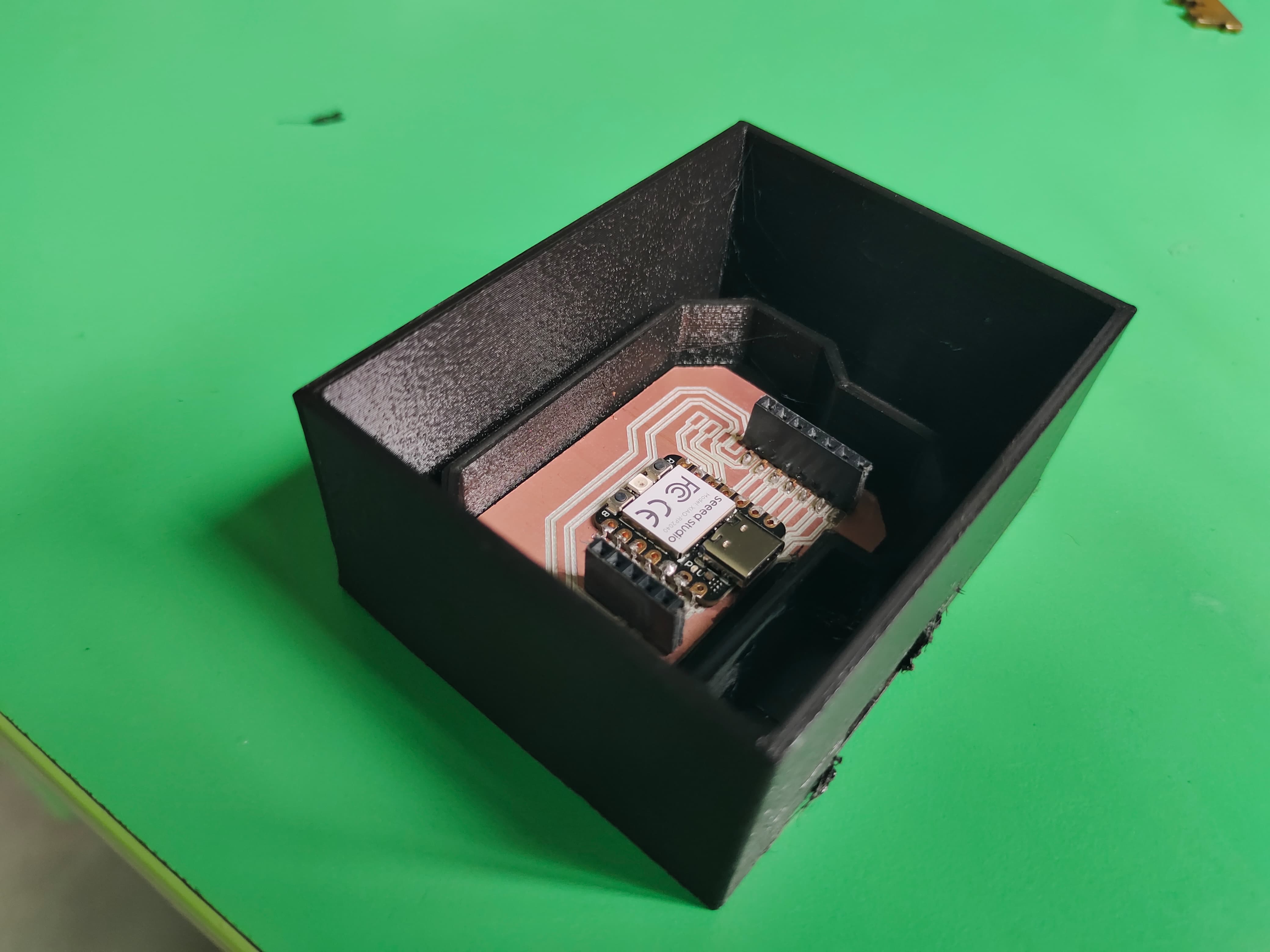
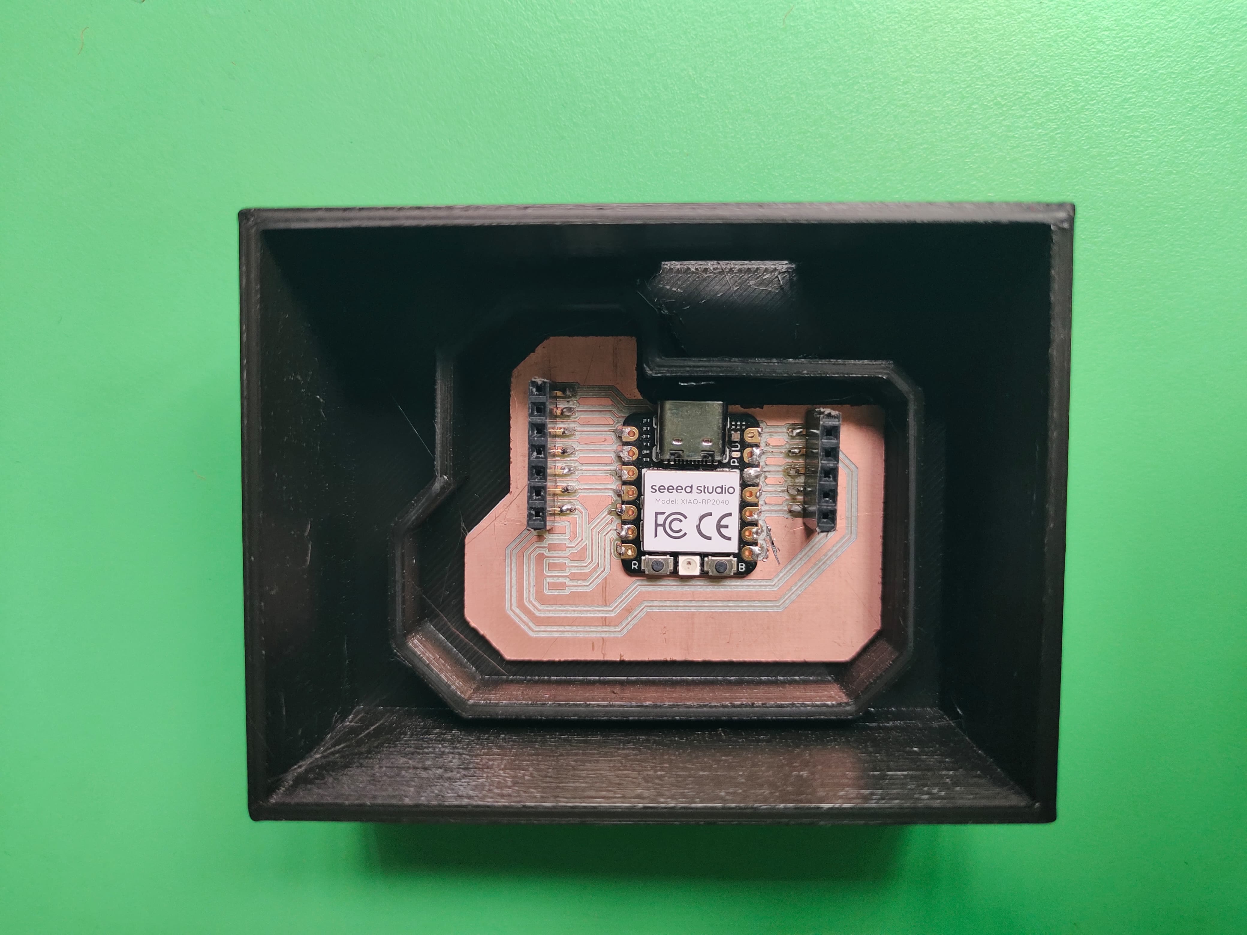
I used the 3D Printing to make the Casing for my PCB, I used SolidWorks for 3D modelling.
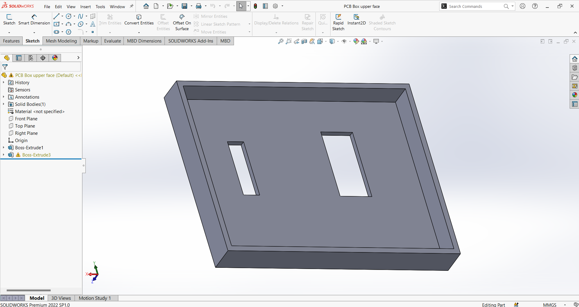
This is the Upper face of the casing.
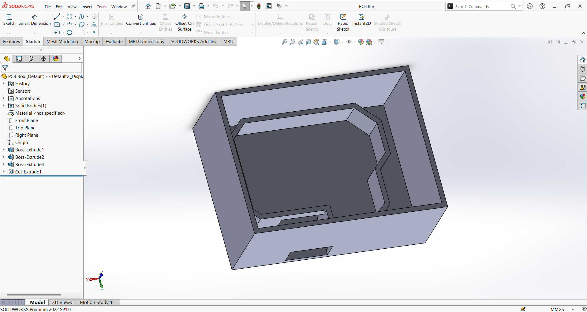
This the box where pcb is going to fix.
Assembly:
Then I Exported the model as .stl file for making the Gcode using Creality Slicer software.
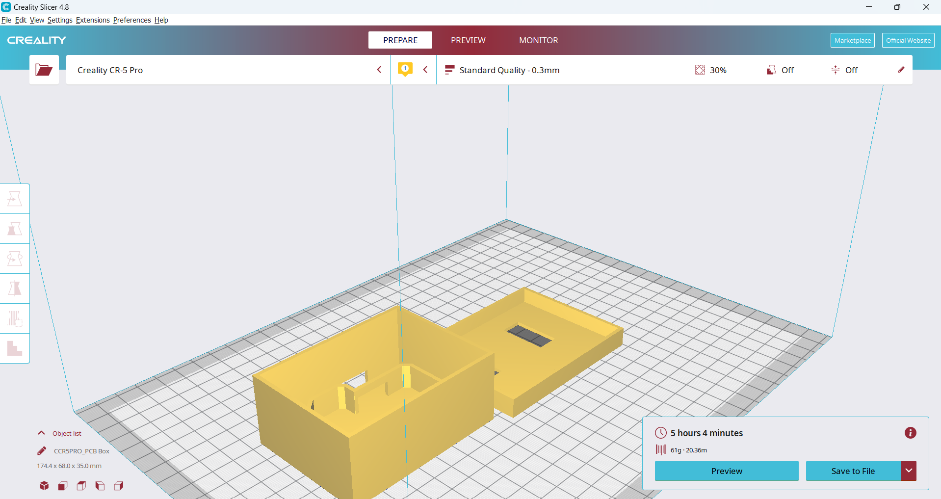
Import the file in software using import option or "CTRL + O".then click on slice option to generate the Gcode.
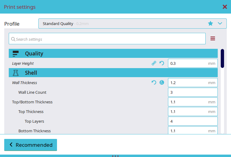
Important Parameters:
1. Layer Height = 0.3mm
2. Wall Thickness = 1.2mm
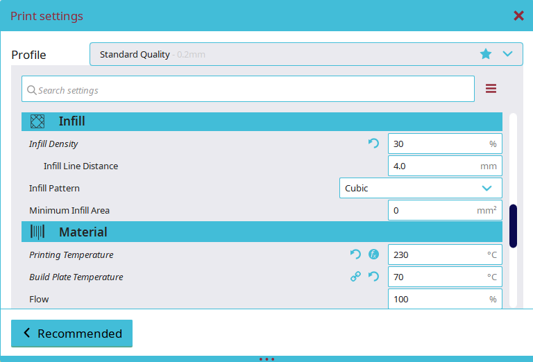
3. Infill Density =30%
4. Bed Temperature = 70 degree celcius
5.Printing Temperature = 230 degree celcius
For 3D Printing I used the PLA Material.
Output:
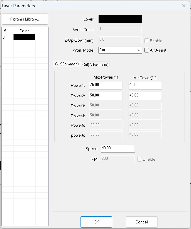
For Laser Cutting I used the Laser Cutting software, Firstly I exported the dxf file of the 3d model from Solidworks using Import Option or "CTRL + I". after uploading for Cardboard of 5mm thickness The Speed and Power is as Follows for our CO2 100W Laser Cutter Machine.
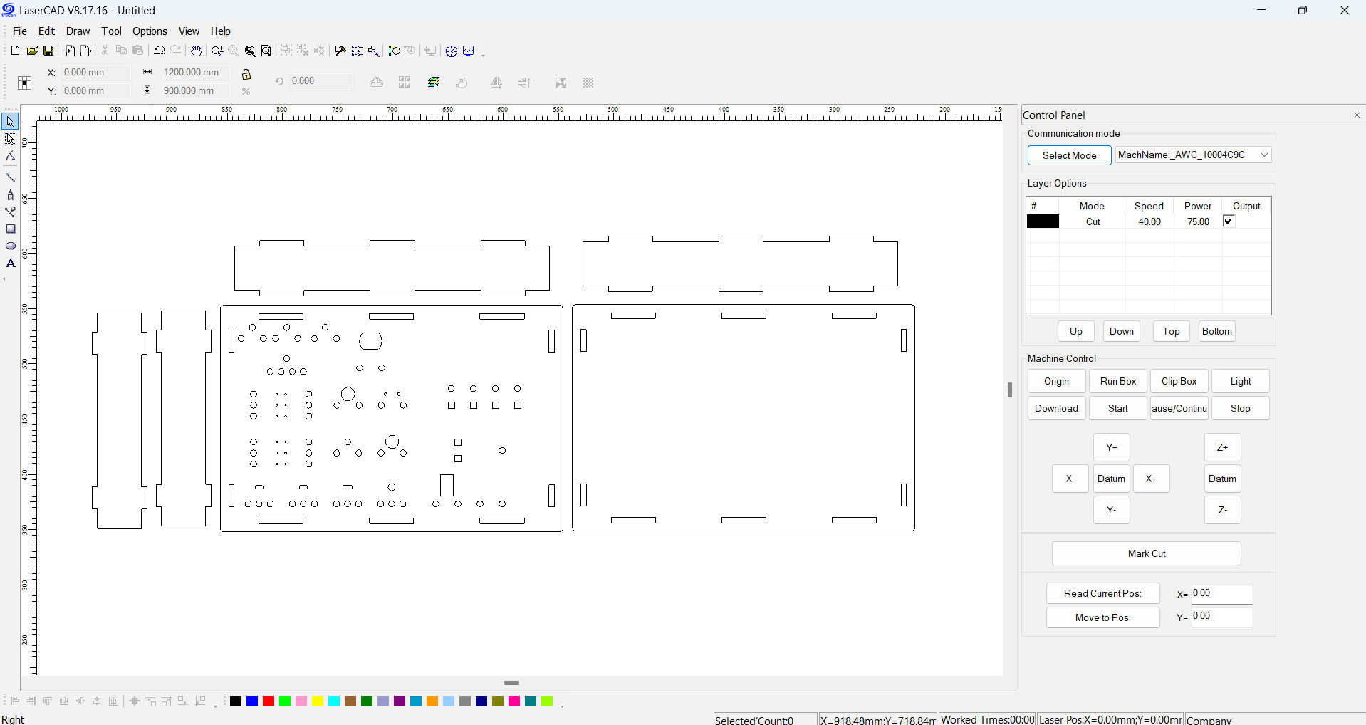
Power: 75
Speed: 40
Then From Select mode option I choose USB mode then I selected the machine connected with my laptop via cable and clicked on download for downloading that code into machine.
#_Output_:)
After Laser Cutting I got this Output
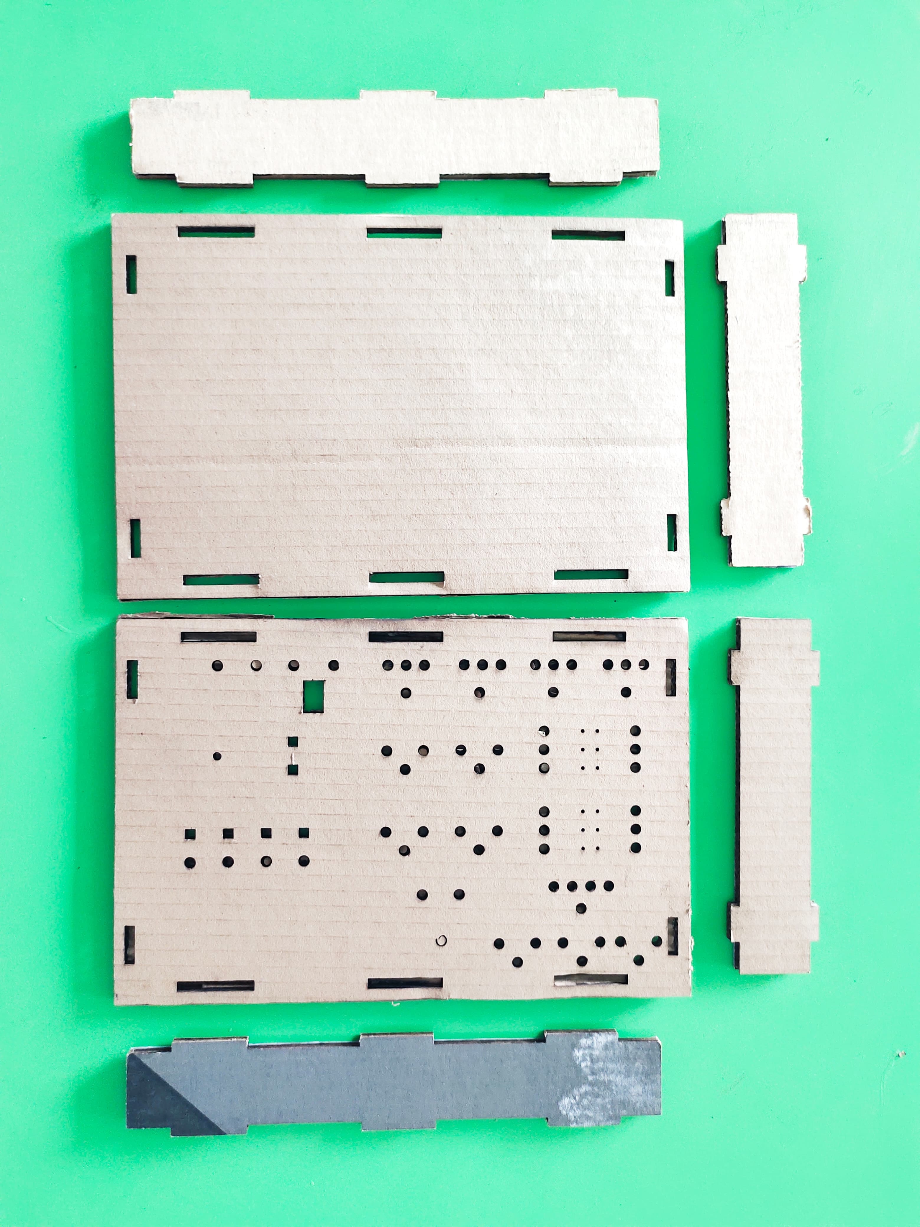
These are the Laser cutted parts.
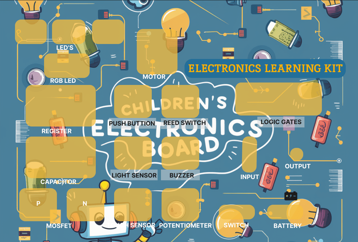
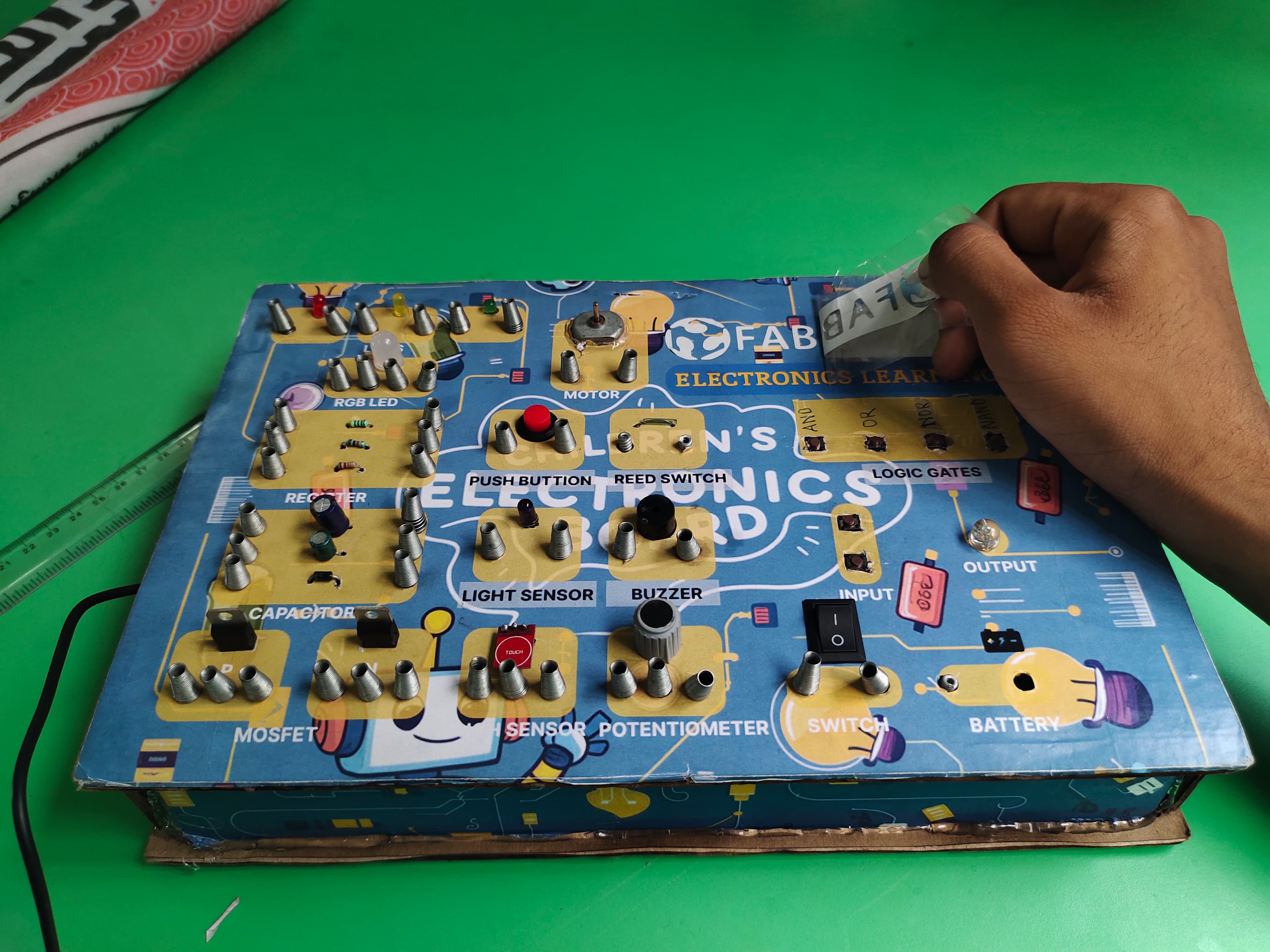
This is the poster that I have designed using Figma, I used Multiple layers option, Different shapes and the background image which is generated by Ideogram by chatgpt.
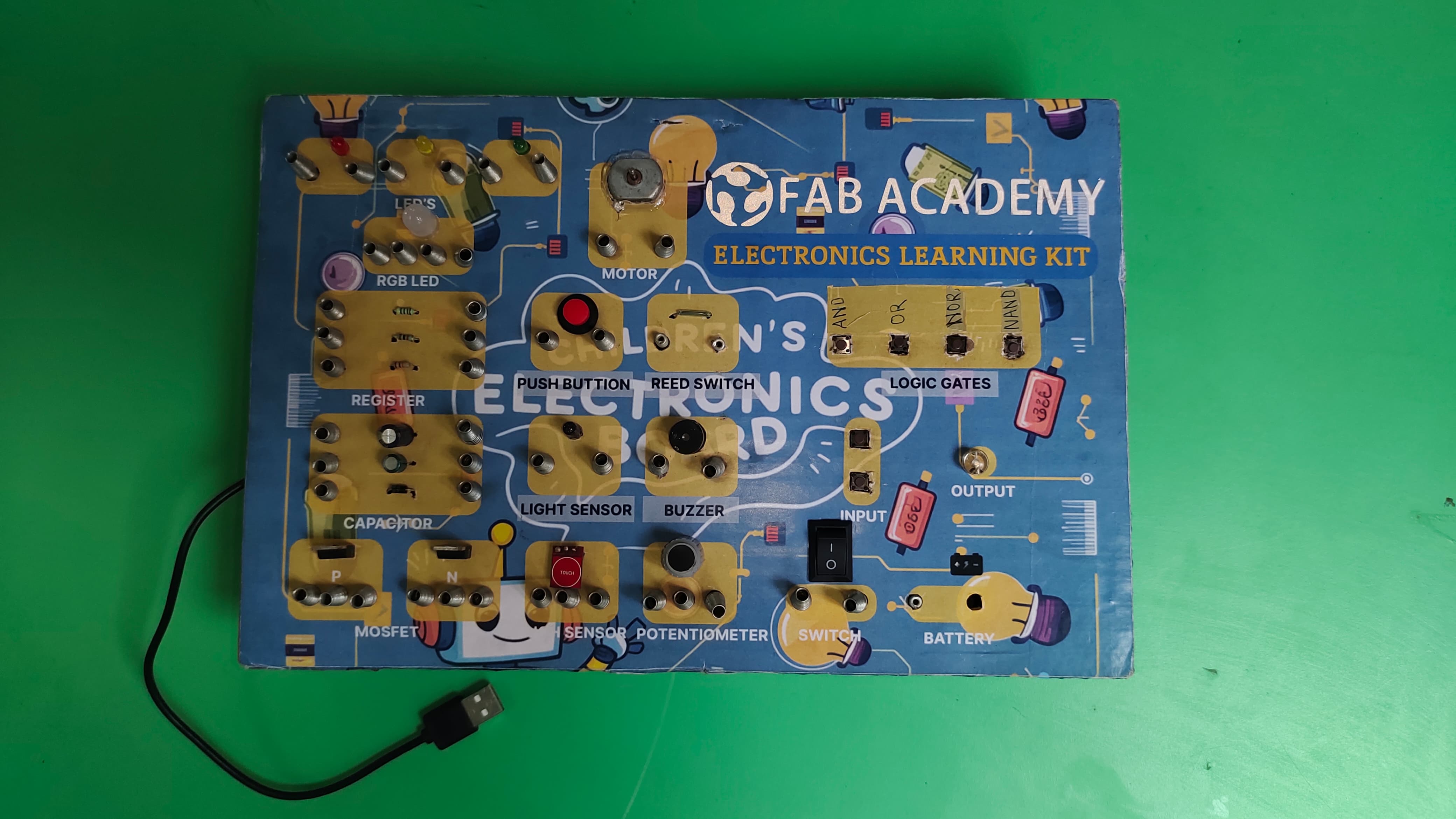
I sticked that poster onto my final kit box.
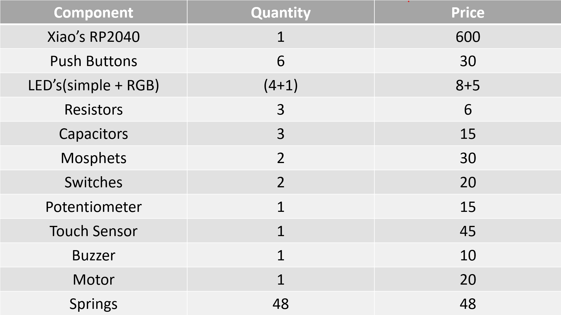
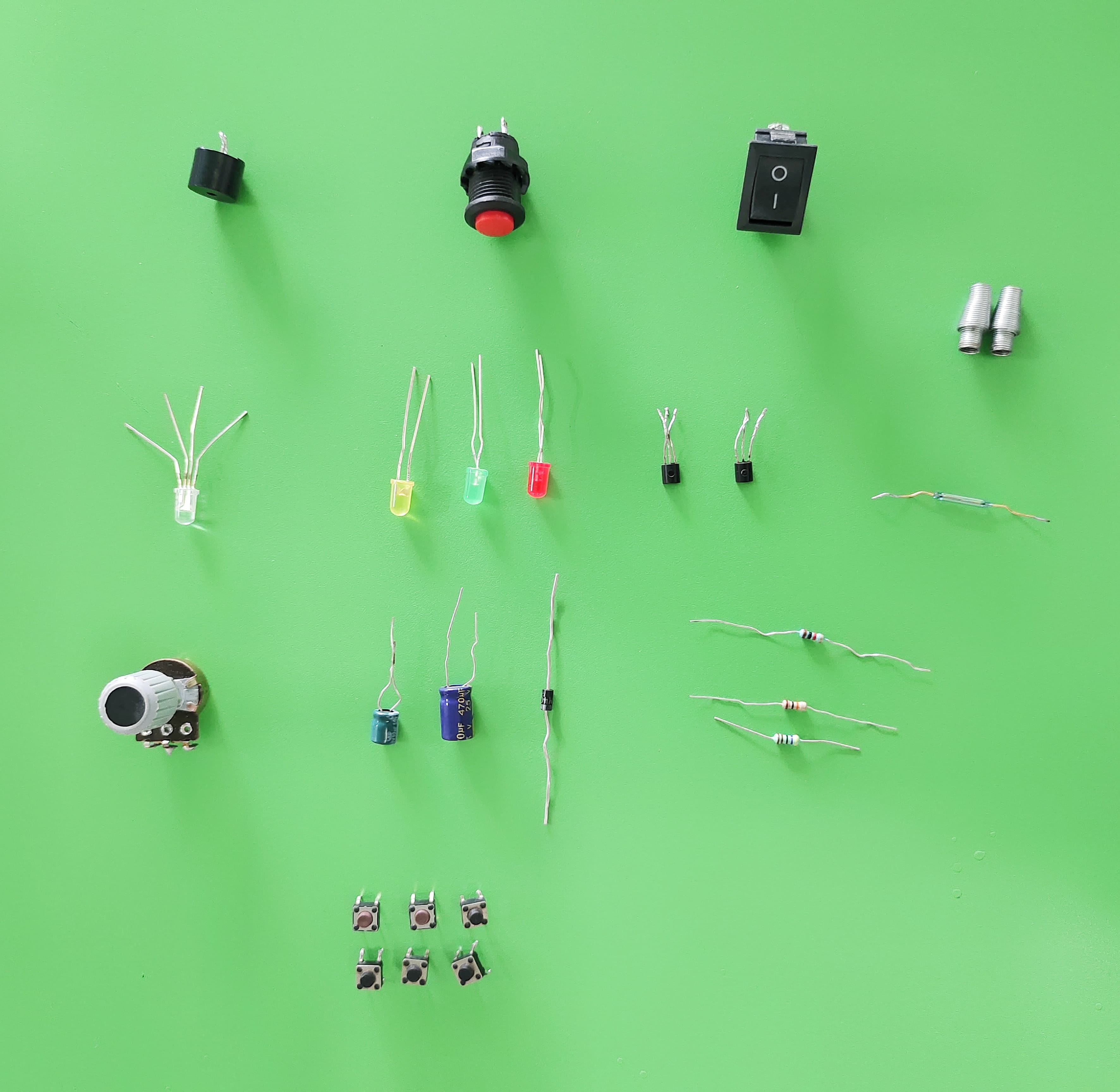
These are the Components that I have used in this project.
Below all the purchase links are provided for the components.
1. Xiao RP2040.
2. LED's.
3. RGB.
4. Buzzer.
5. Push Buttons.
6. Switches.
7. Potentiometer.
8. Touch Sensor.
9. DC motor.
10. Resistors.
11. Capacitors.
12. Mosfets.
Components
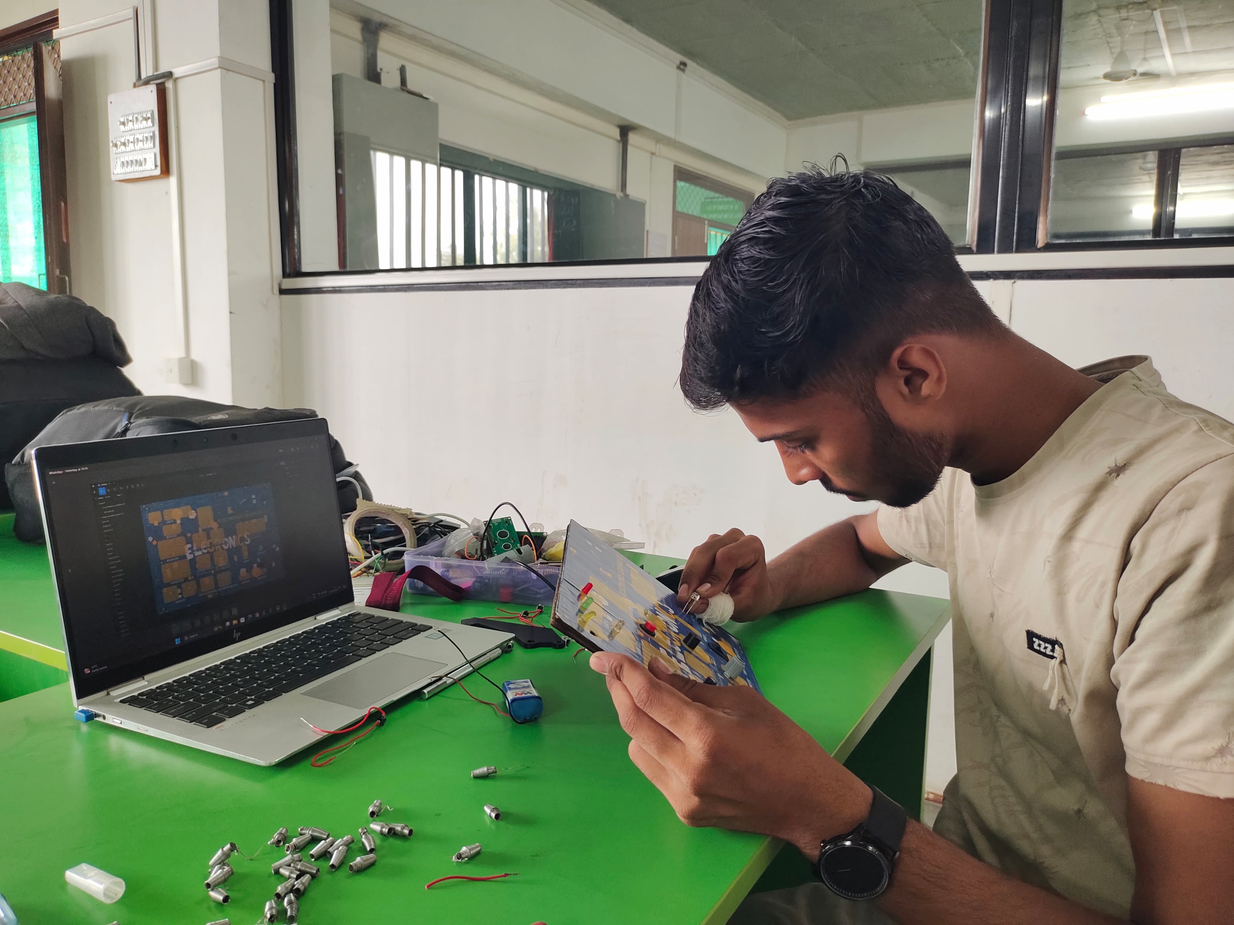
I starded fixing all the components on the board
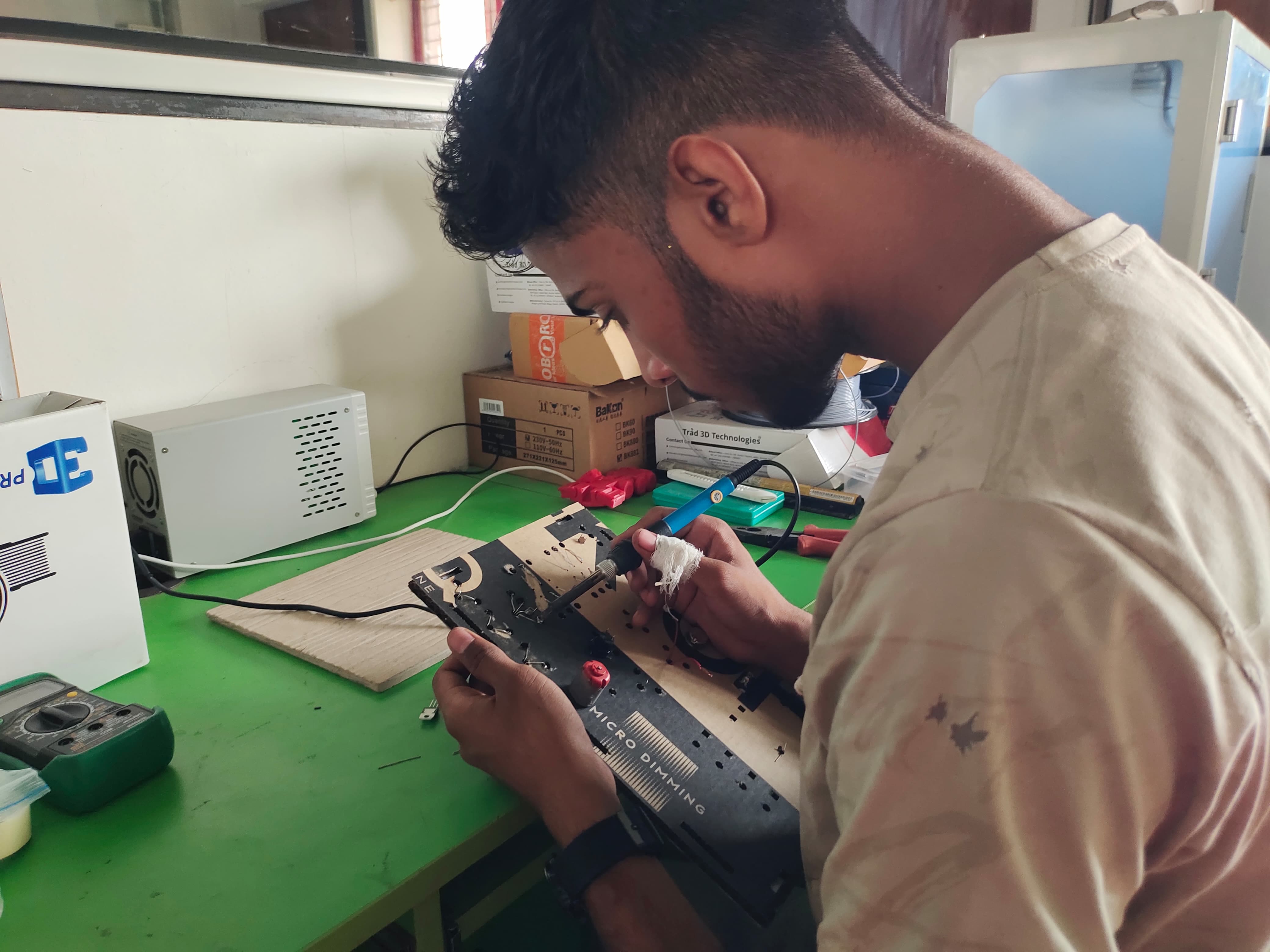
I started soldering the components.
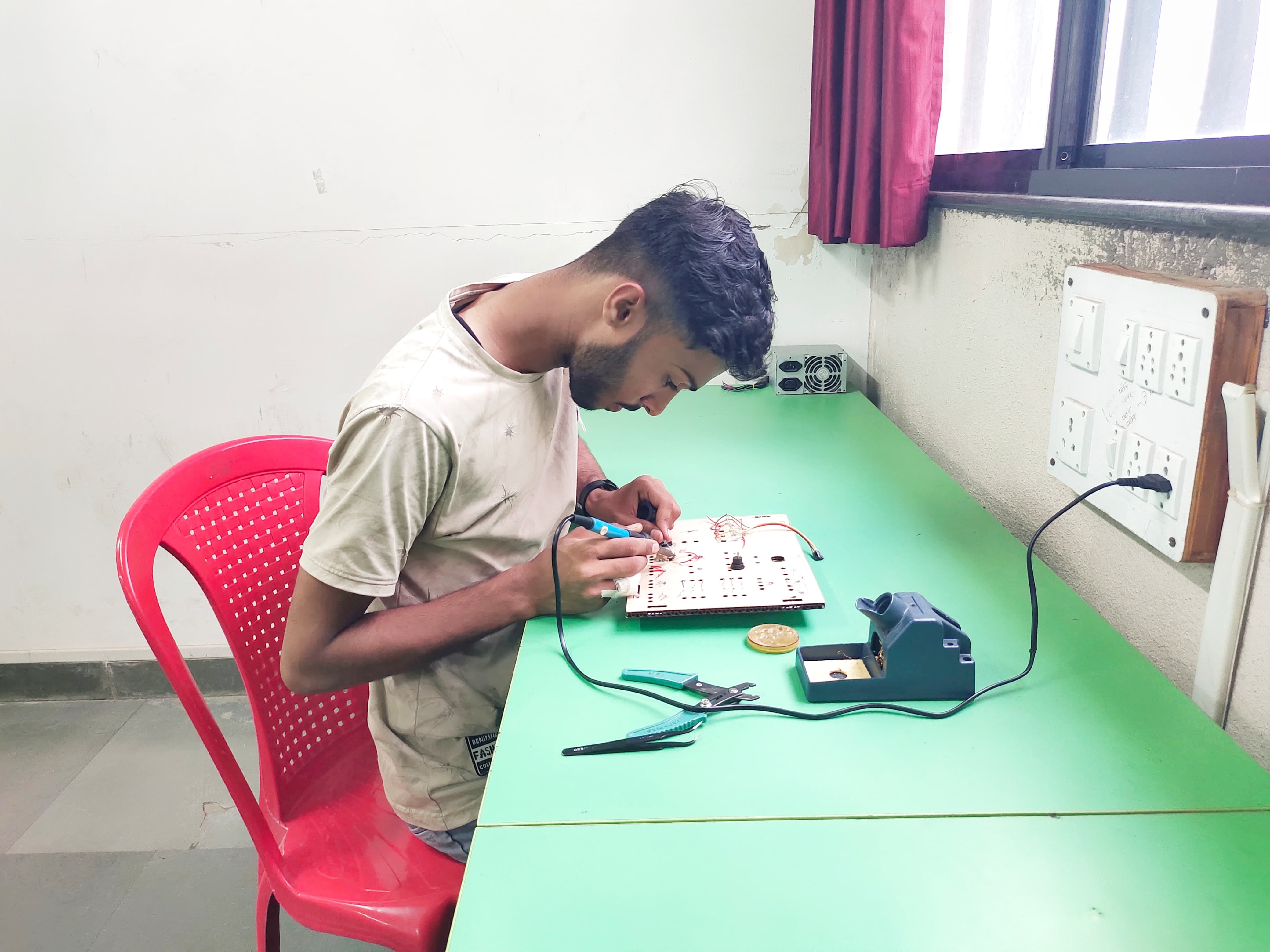
All the components are soldered with the springs by which the students can able to make the connections.
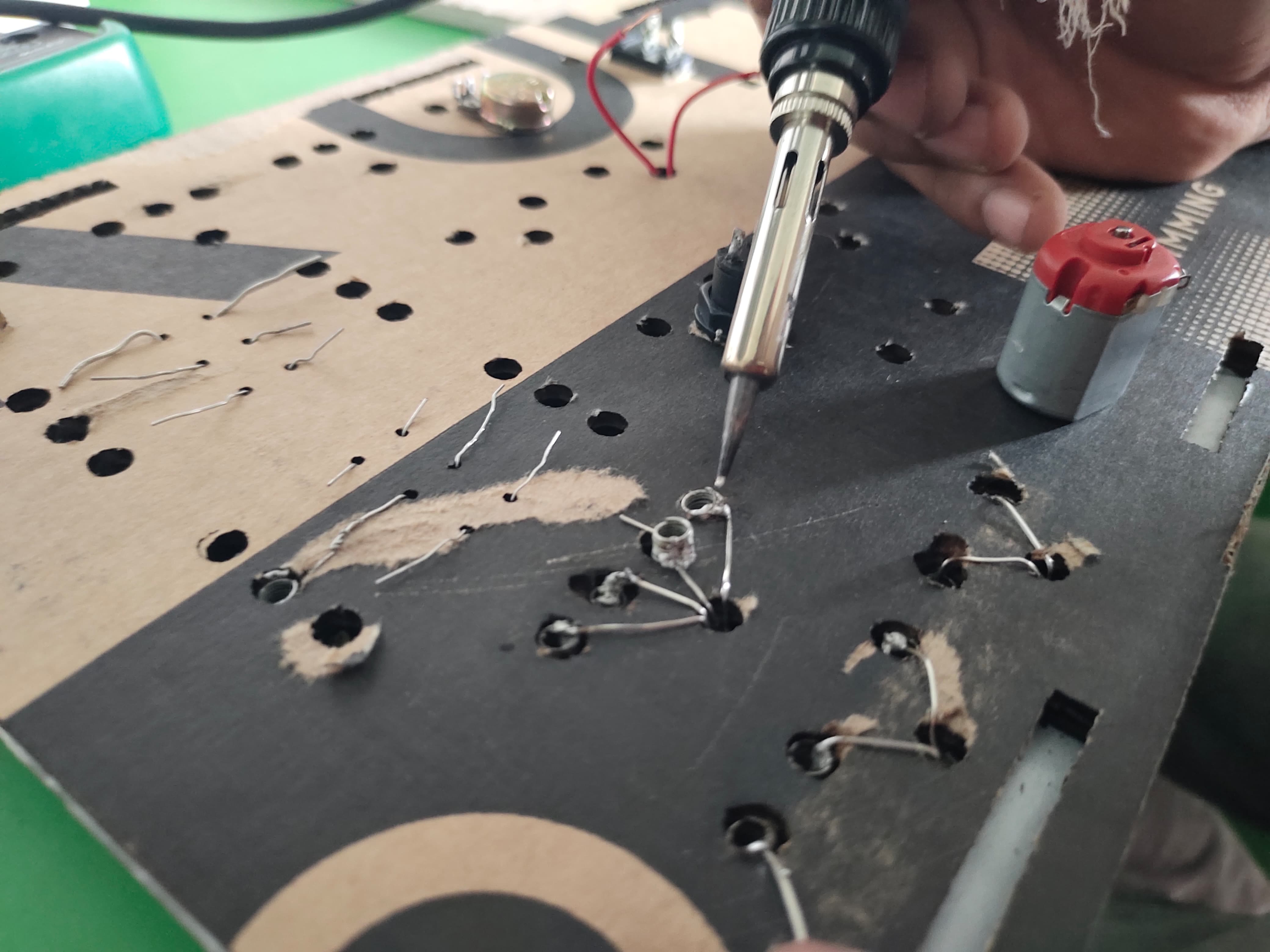
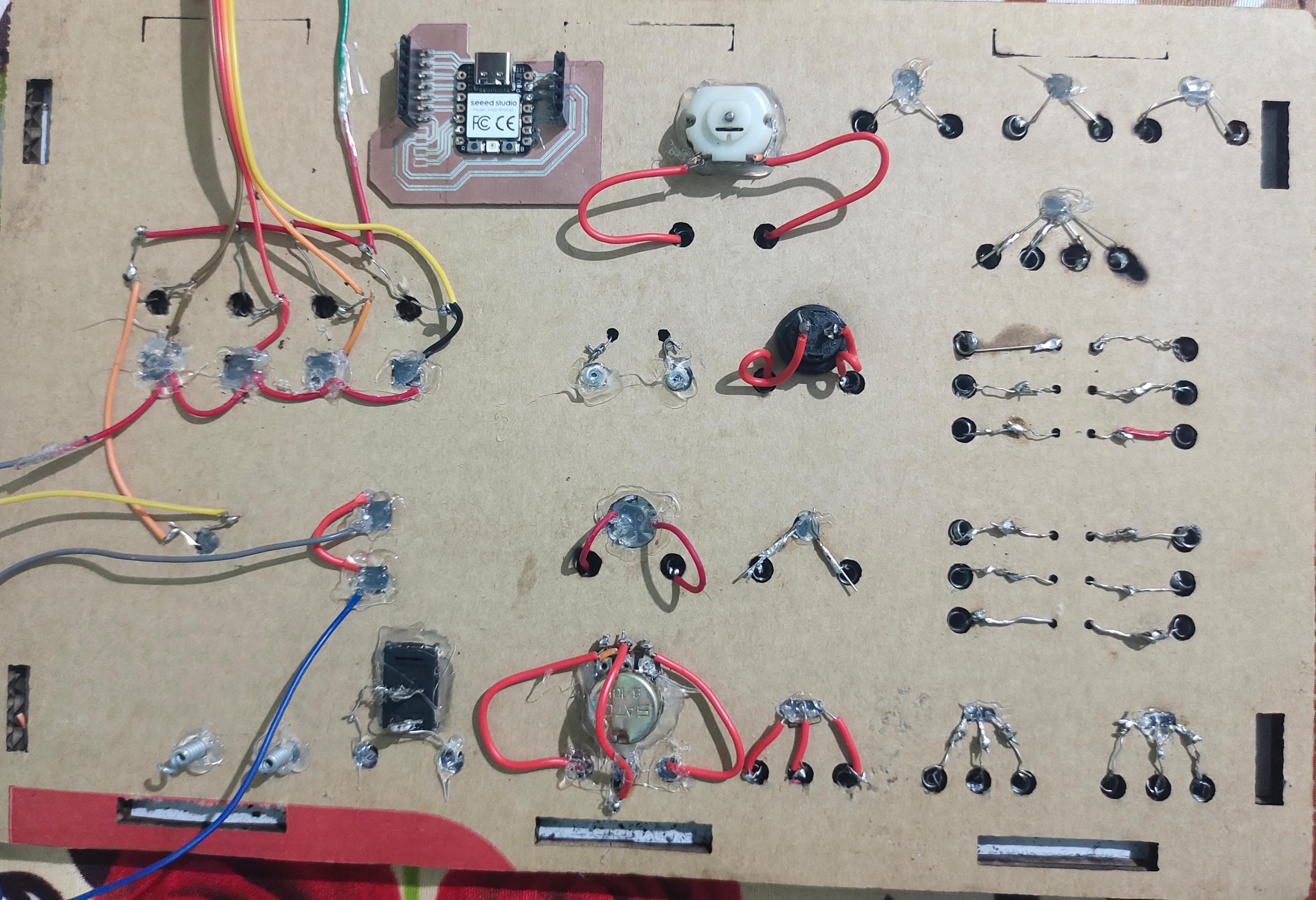
This is the board looks like from inside after soldering
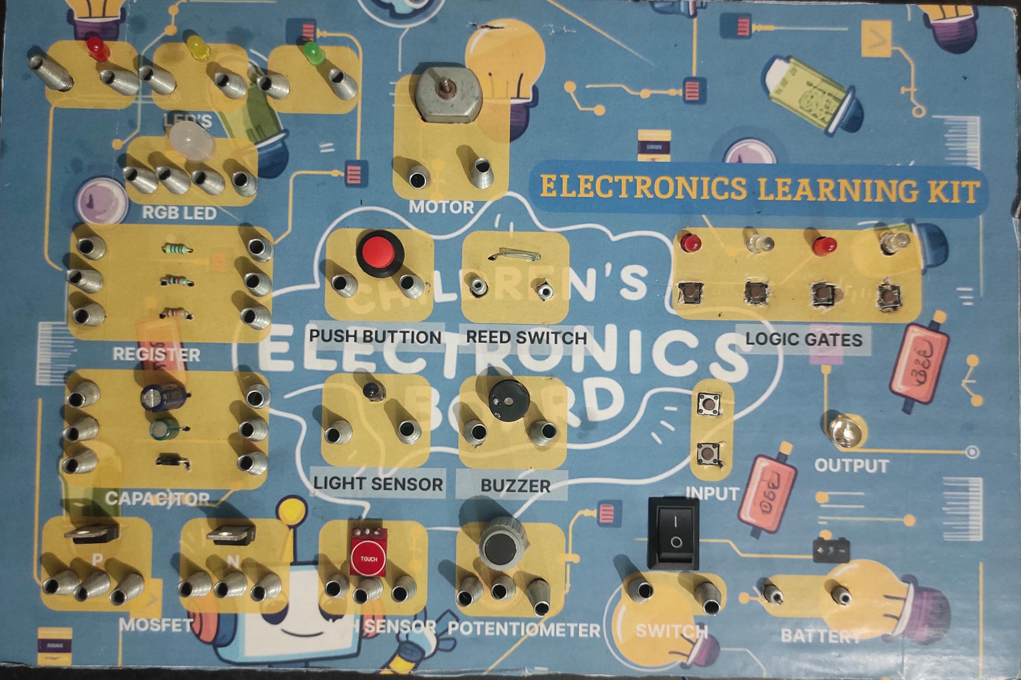
This is the board looks like from outside after placing the components and soldering them.
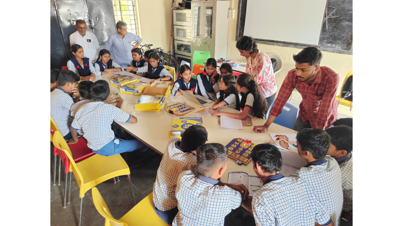
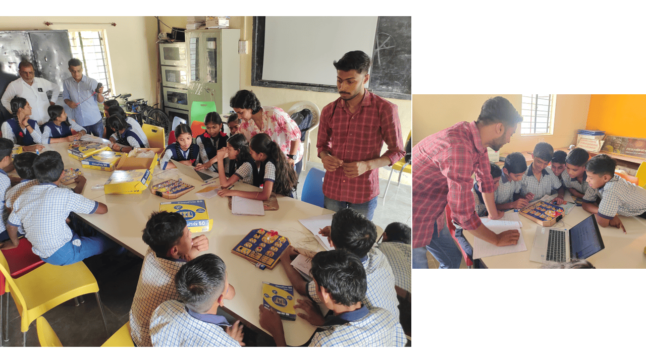
I gave this Electronics Learning Kit to the students, and they were playing with it very interestingly.


Electronics Learning Kit by Akash Mhais is licensed under CC BY-NC 4.0![]()
![]()
![]()
Akash Mhais FAB ACADEMY