Week8: Electronic design
This week we were working on Electronic design - PCB design and in the group we had to test our microcontroller circuti board with lab equipment. This week, we focused on electronic design, specifically PCB design. PCB stands for Printed Circuit Board, which is a crucial component in electronic devices. A PCB connects electronic components and provides a pathway for electrical signals to travel between them, ensuring efficient communication and functionality within the device.
Group work
Our group assignment was to use the test equipment in our lab to observe the operation of a microcontroller circuit board and to send a PCB design out to a board house for manufacturing. Group work can be found by opening the link here.
Individual Reflection:
- Multimeter Skills: I improved my skills in using a multimeter to measure various electrical parameters such as voltage, current, and continuity. This is essential for verifying proper circuit operation and troubleshooting issues.
- Oscilloscope Proficiency: I gained hands-on experience with an oscilloscope, learning how to set it up, connect probes, and interpret the displayed waveforms. Observing the microcontroller's output signals in real-time helped me understand how the microcontroller interacts with external components.
- Signal Analysis: By analyzing the waveforms on the oscilloscope, I learned how to identify key characteristics of digital signals, such as frequency, duty cycle, and amplitude. This knowledge is crucial for debugging and optimizing microcontroller applications.
- Practical Application: The assignment provided practical experience in setting up test equipment, connecting it to a microcontroller circuit, and interpreting the results. This practical approach reinforced theoretical knowledge and improved my problem-solving skills.
- Importance of Documentation: Documenting the setup, measurements, and observations on the group work page emphasized the importance of clear and detailed documentation in engineering tasks. This ensures that the work can be replicated and understood by others.
About my assignment
What to do?
Question: use an EDA tool to design a development board to interact and communicate with an embedded microcontroller, produce it, and test it
To do my assignement I used KiCad Software to develop my PCB from schematic design to PCB design and saving printable files.
kiCad KiCad is an open-source software suite for electronic design automation (EDA), primarily used for designing printed circuit boards (PCBs). It includes tools for schematic capture, PCB layout, and 3D viewing. KiCad is available for Windows, macOS, and Linux, making it accessible to a wide range of users.
We started by downloading the software from the link here: https://www.kicad.org/download/windows/. Downloaded Worldwide setup from gitHub.
Downloaded version of kiCad
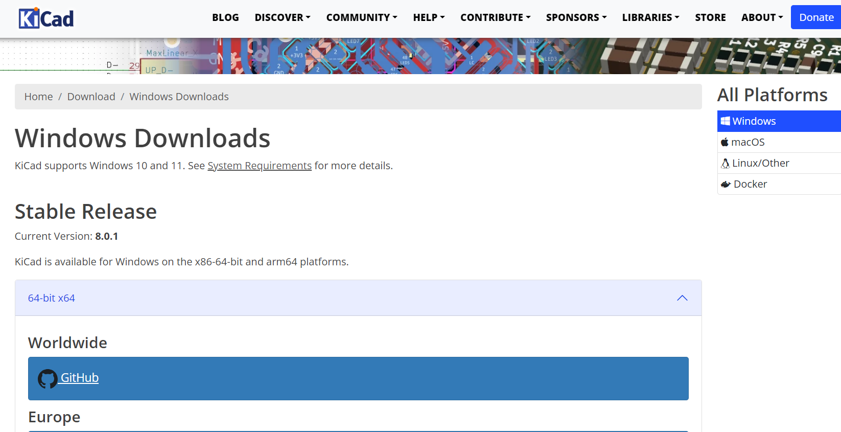
I downloaded version of kiCad which is 8.0 as the latest from the link above. Clicking on GitHub, the setup directly downloads.
Installation of kiCad, double click on the setup.
Installation of kiCad on my computer.

After following default process, then finish installation

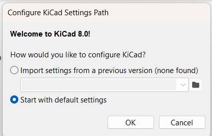
Opening Kicad at the first time, started by default setting
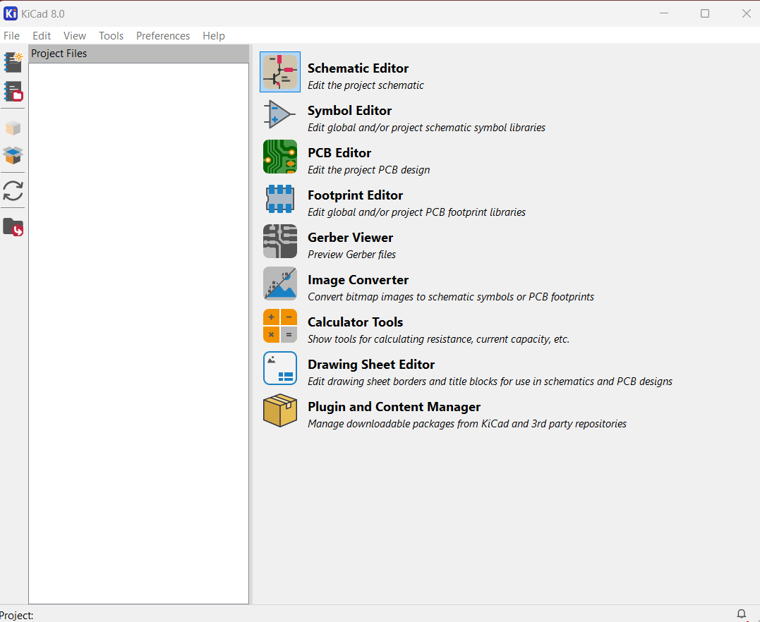
This is the page that comes after opening Kicad software
MY DESIGN IN KICAD
Schematic Design, PCB Design, Printing, Soldering and Testing
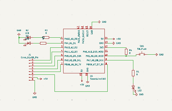
Placing of components in schematic design
Click on symbol on the right corner and search of tools symbols in popup

Joining components by wire symbol shown on image below

Finished joining components of my schematic design
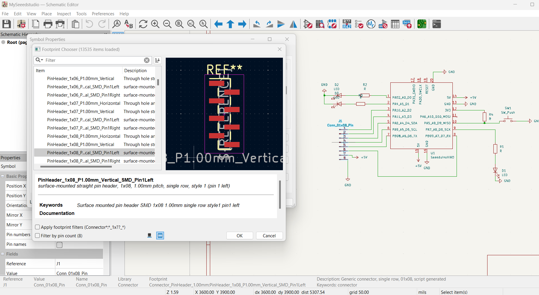
Assign footprint to each component in Schematic design

Continue assigning footprint (pinheader)
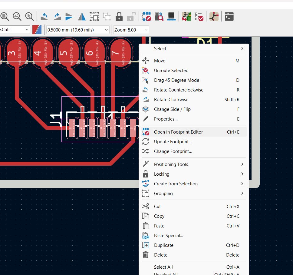
Edditing footprint (open in footprint edditor)
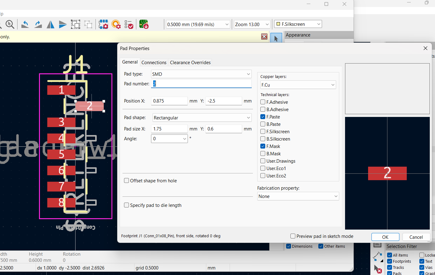
Inverting pad to same direction
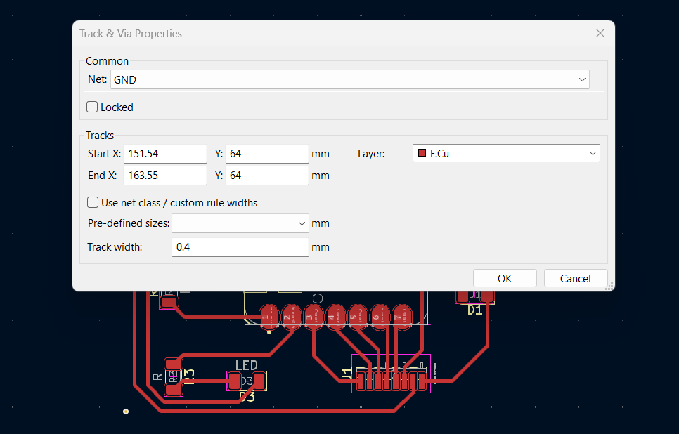
Edditing Trace line size to 0.4mm
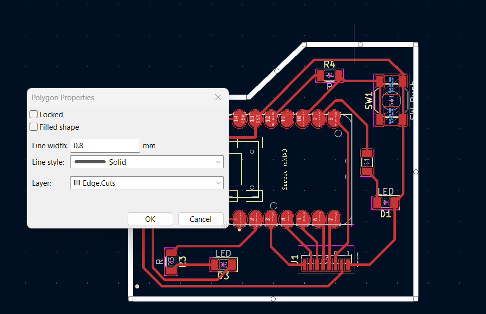
Drawing the edgecut with polygon shape
Edditing the line width of edgecut
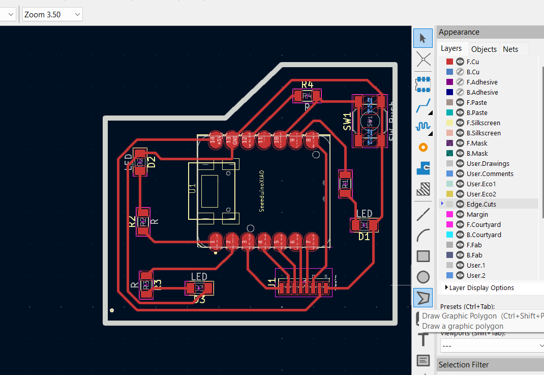
Final PCB Design of my design

Produced 3D view of my PCB design

Printing PCB
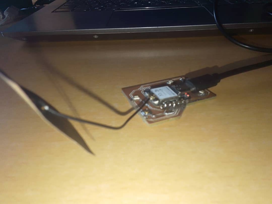
Milling, Drilling, soldering components and testing
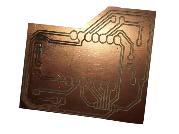
After printing, it came out like this
After soldering components