Week4: Electronics Production
About the assignment
PCB (Printed Circuit Board) fabrication
Microcontroller development board
I. PCB (Printed Circuit Board) fabrication
Definitions
PCB (Printed circuit board): It is a board made of a non-conductive material, such as fiberglass, with conductive pathways printed or etched onto it. PCBs are used to mechanically support and electrically connect electronic components using conductive tracks, pads, and other features etched from copper sheets laminated onto the substrate.
PCBs are found in almost all electronic devices, providing a reliable and compact way to interconnect components.
Microcontroller: A microcontroller is a compact integrated circuit designed to govern a specific operation in an embedded system. It contains a processor core, memory, and programmable input/output peripherals, all on a single chip.
Microcontrollers are used in automatically controlled products and devices, such as automobile engine control systems, remote controls, office machines, appliances, power tools, toys, and other embedded systems.
Roland SRM-20(PCB Drilling And Milling Machine)
The following is the machine we used in printing our PCP in group and in personal.
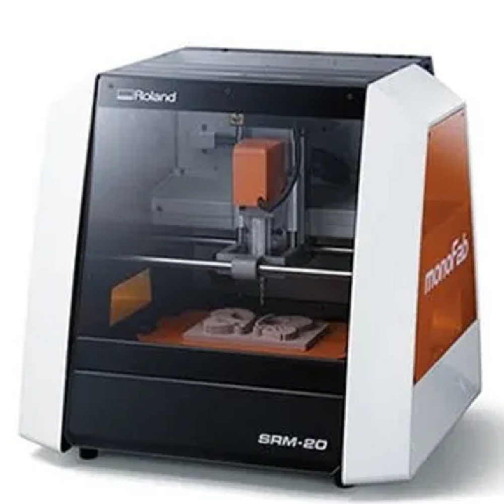
Roland milling machines enable engineers and designers to produce highly accurate, functional parts and snap-fit prototypes quickly and inexpensively from a wide range of materials and software. Roland’s MDX and monoFab brands go beyond the capabilities of 3D printing to provide clean and precise subtractive milling results that brings your 3D designs to life and capture the imagination.
GROUP WORK
In the group we started the assignment, with images shown in class of electronics production
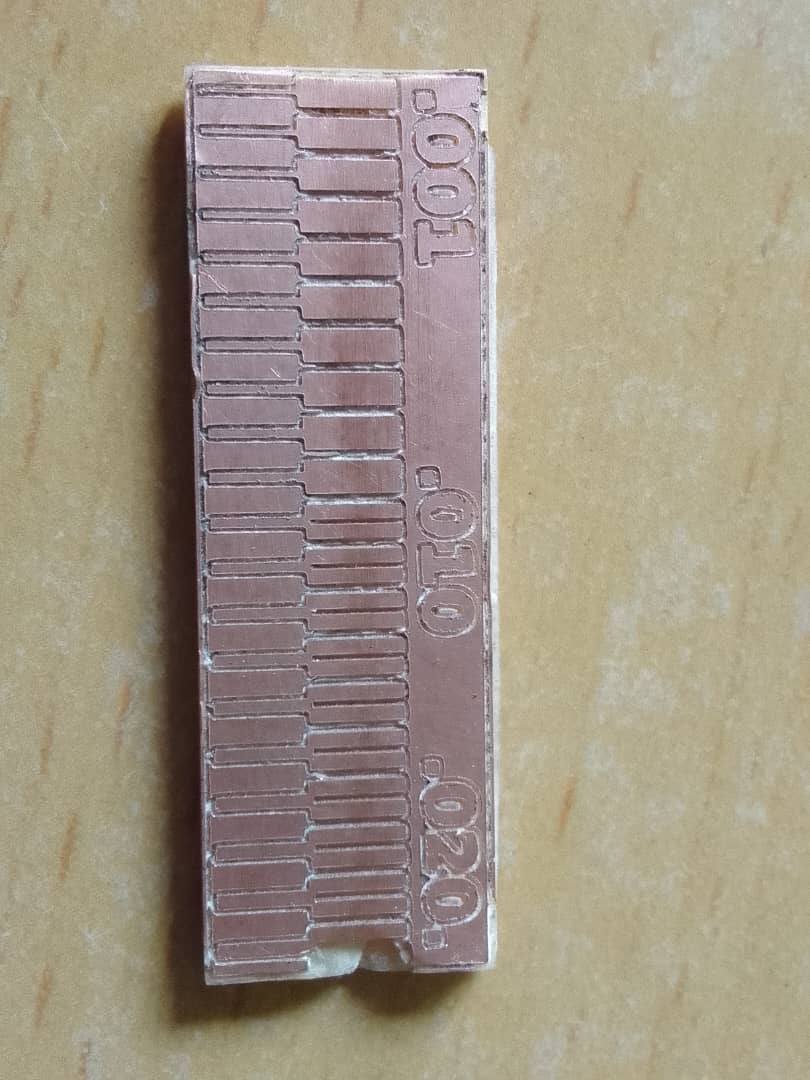
The part used in the assignement is here.
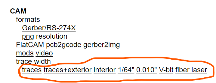
We started by downloading the files on the above image for interior and traces. The following steps were applied to both the images below. We used two different bits for cutting interior and tracing. For tracing we used V_shaped bit of 0.254mm diameter with cutting angle of 60 degree and we used End mill bit with a ring of 0.254mm diameter for outlining the PCB.
The online software we used to produce the file the is read by the PCB printing machine is on the link can be found here..

The process explained with the images below.
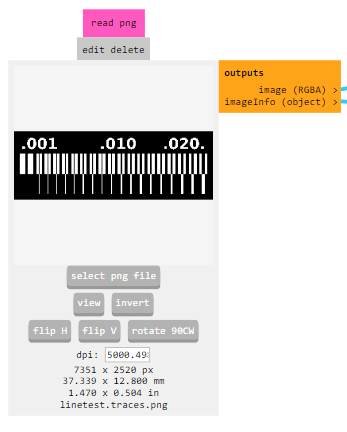
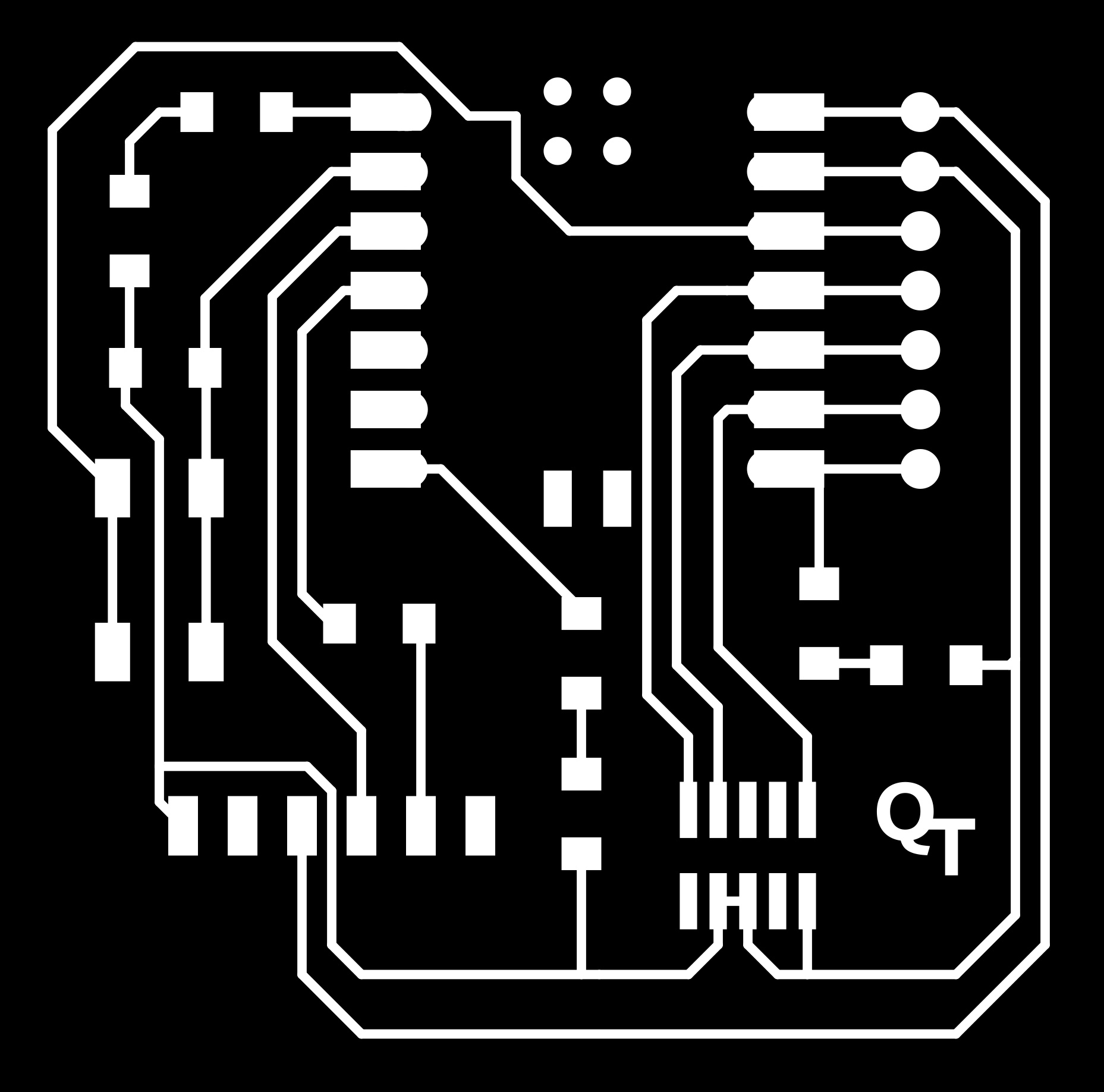
The image of traces for the PCB.
The image outline of the PCB.

Selecting png image to the software as shown below.
Edditing trace bit as the bit we have which is 0.254cm as shown below.
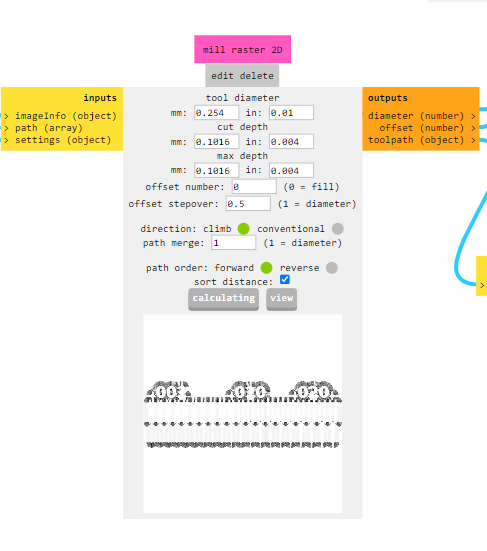
Puting coordinates xyz to zero as shown below.
When I click calcuate on mill raster 2D the image immediately downloads as shown below.
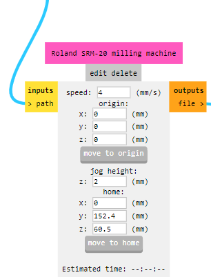
The next step is to set the machine.
Puting on the PCB Machine and connecting the cable to the machine.Making sure the software that reads the file above is ready.The software is VPanel for SRM_20. The software can be downladed on the link here.Click here to open the link.
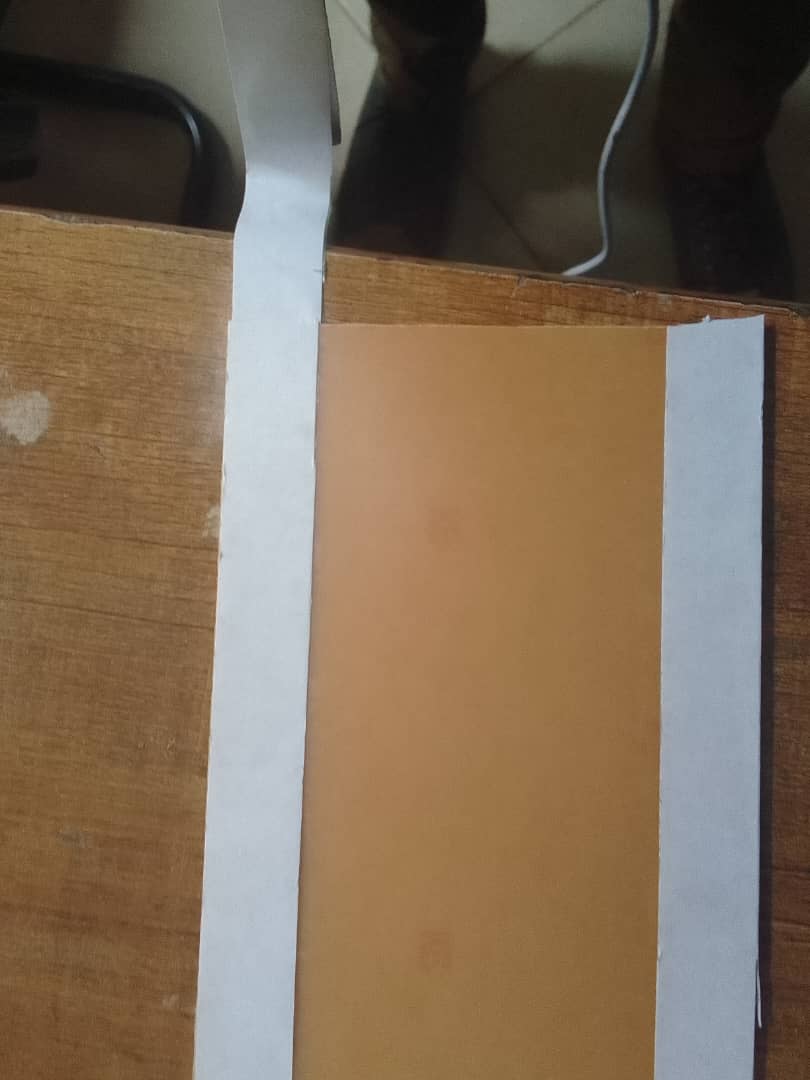
The next step is to make the PCB ready and fixing on the bed.
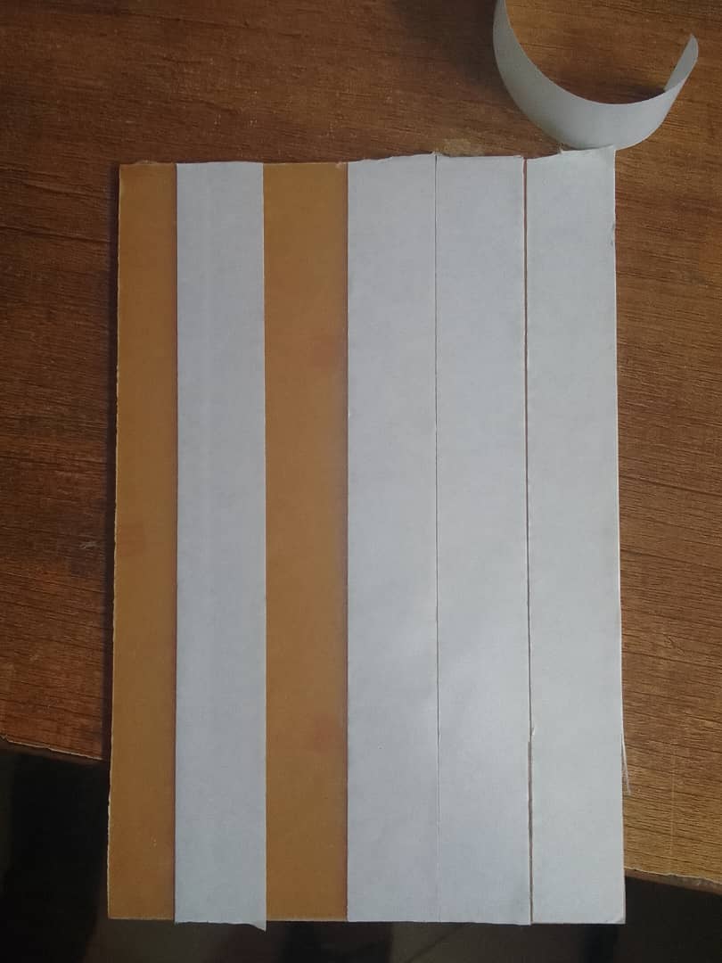
Puting double_sided sticker at the bottom.
Continuation of placing stickers.
Continuation until the bottom is full.
Remove the upper paper on the sticker and fix it on the bed.
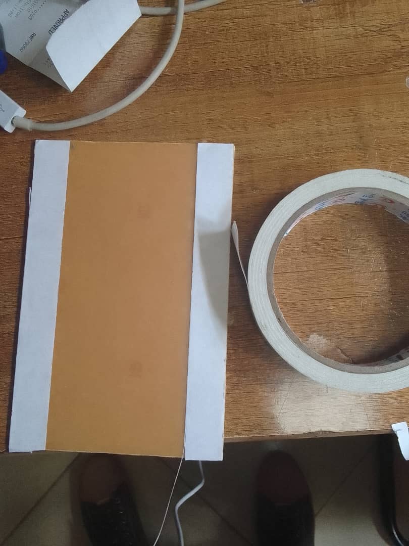
Fixing PCB on the bed.
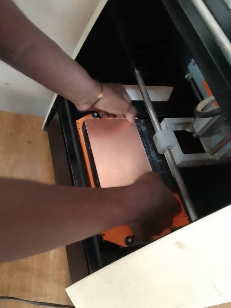
Fixing with pressure on the bed.
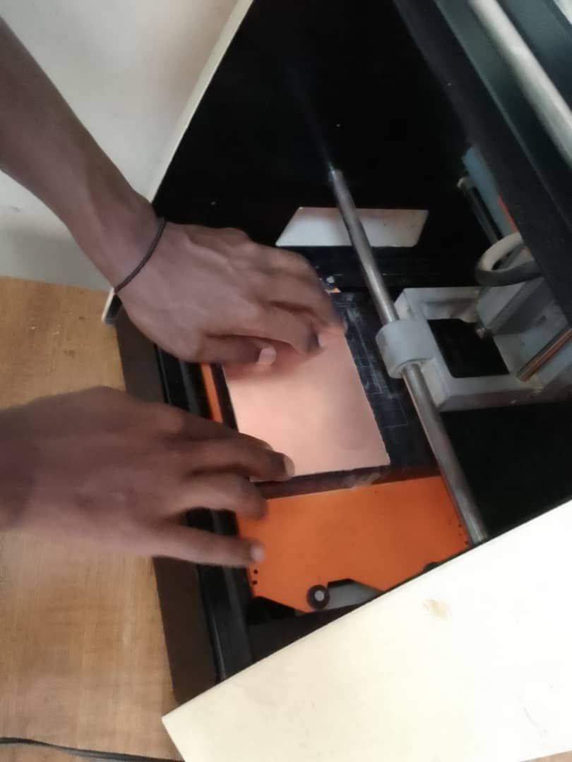
The PCB is ready.
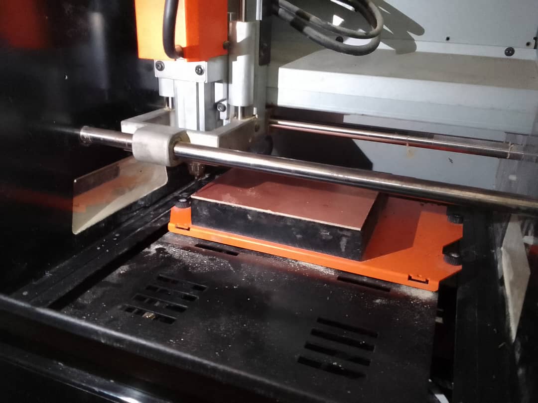
Fixing the bit.
Making the machine ready to print.
Steps shown in the images below.
Opening the software
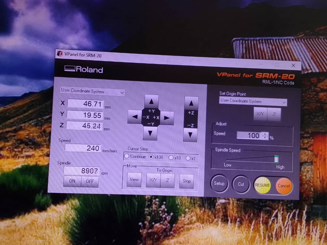
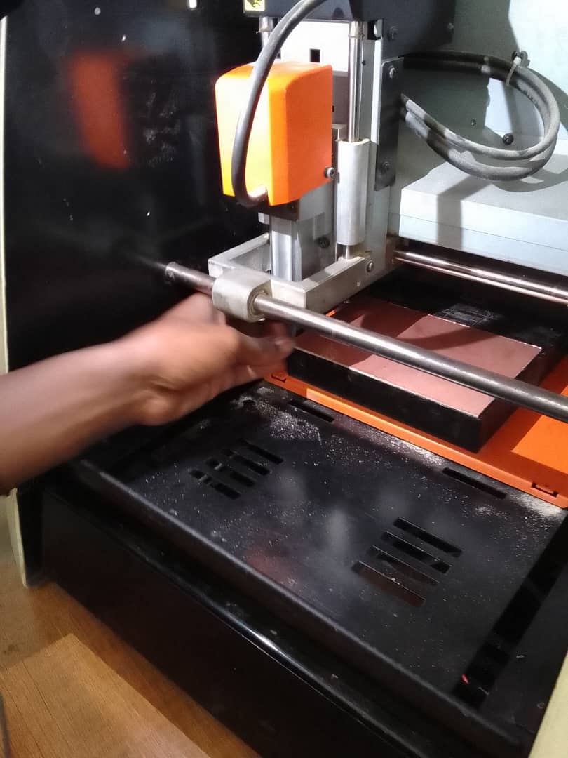
Moving the bit and bed in X,Y and Z until it reaches the starting point.
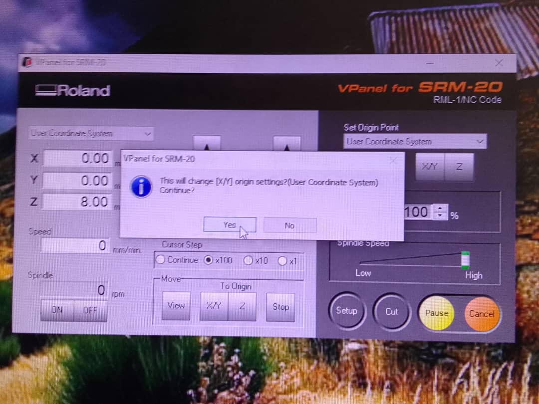
Setting the orgin of X and Y axis.
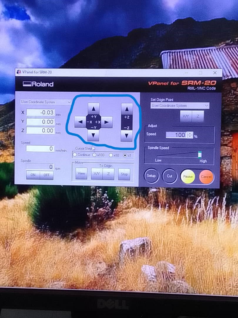
Losening the drill abit to touch the surface and re-fix it to help set the orgin on the surface.

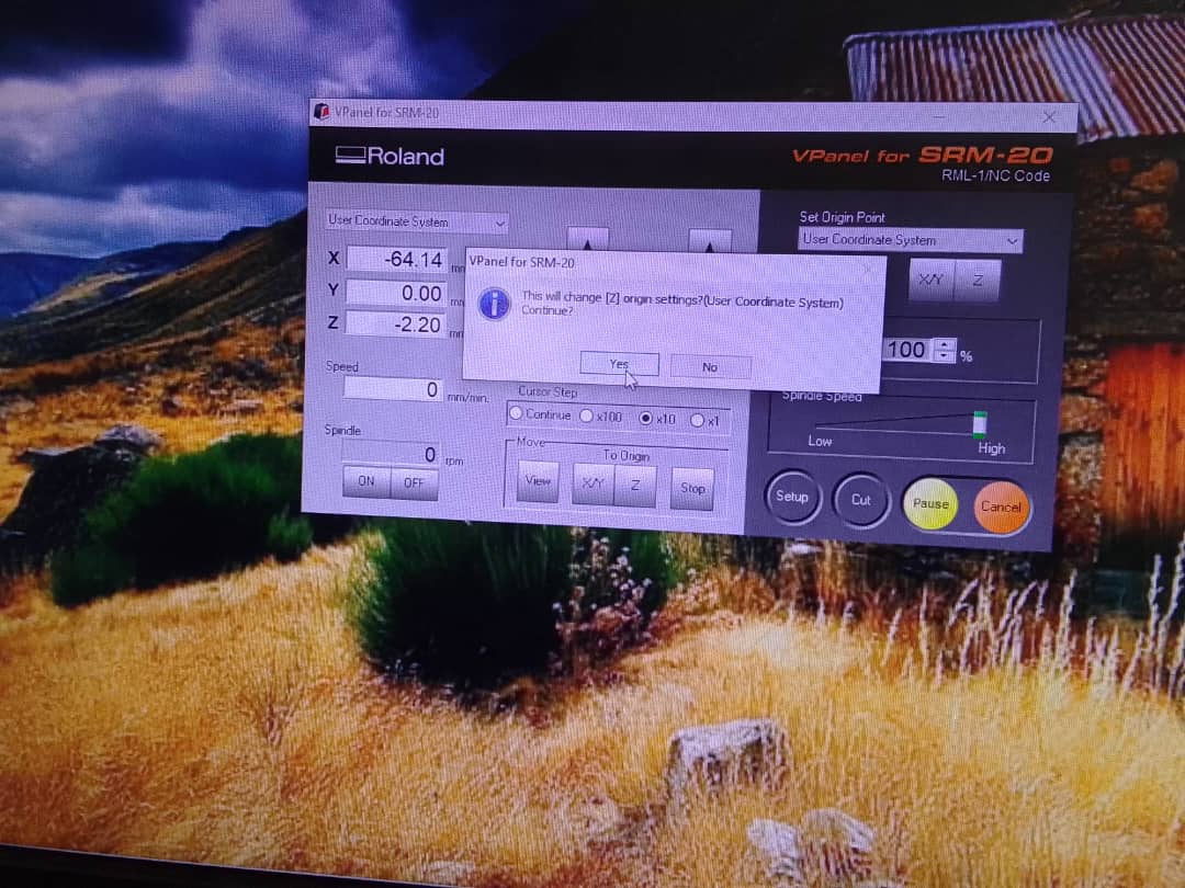
Setting the orgin of Z axis.
Note: Move the Z up by click from the PCB surface to avoid the breakage of the bit as you start printing.
Now start to print.
Now click on cut.
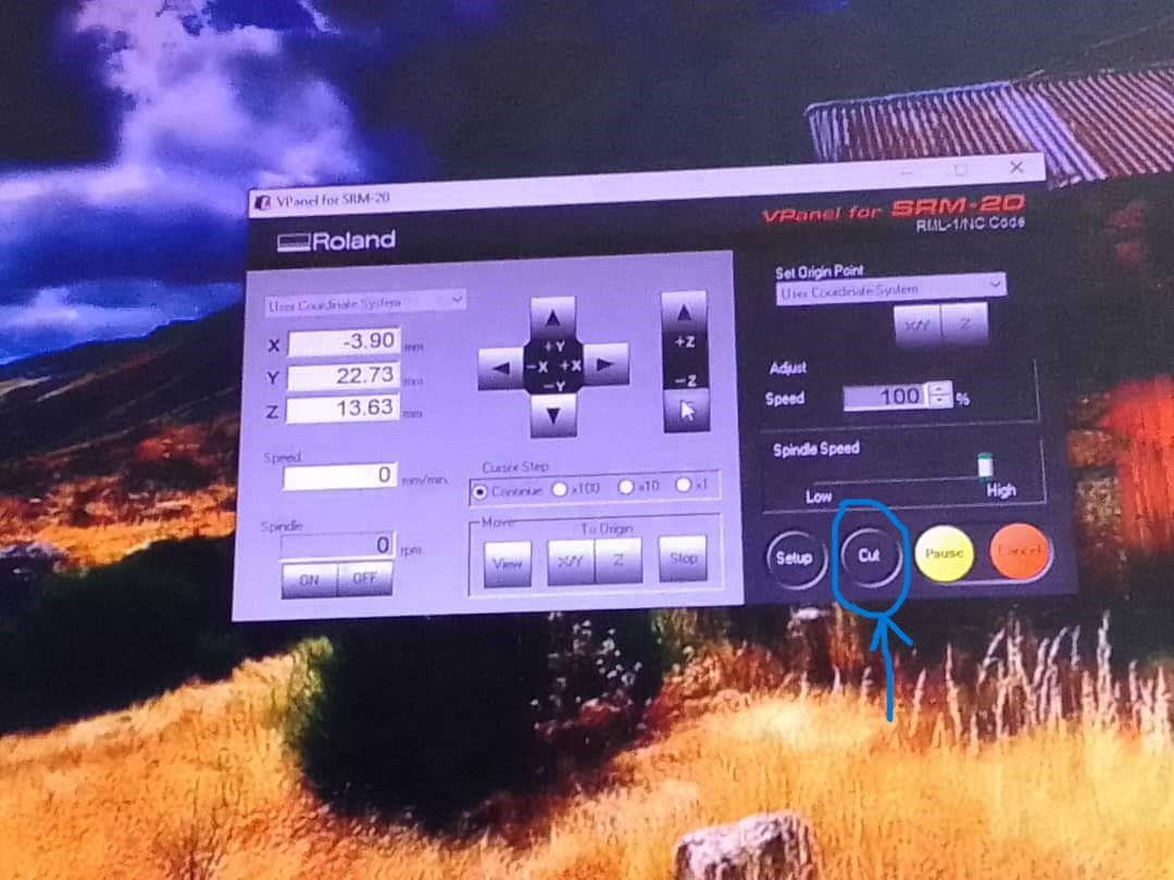
If there is anything in the drop box you can click delete all and then click add to chose a file from the directory.
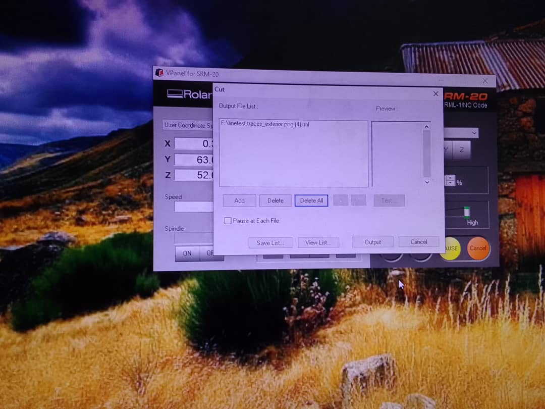
Click output to start printing.

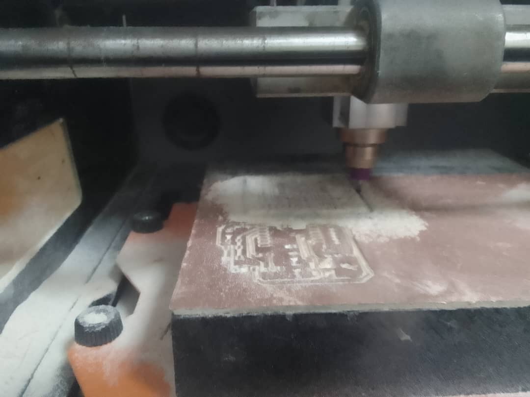
The machine starts printing.
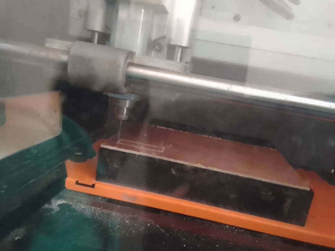
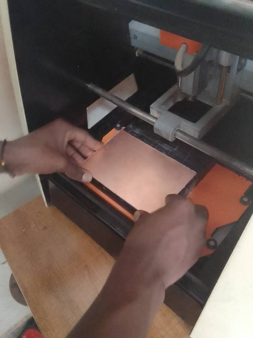
This is the printed design.
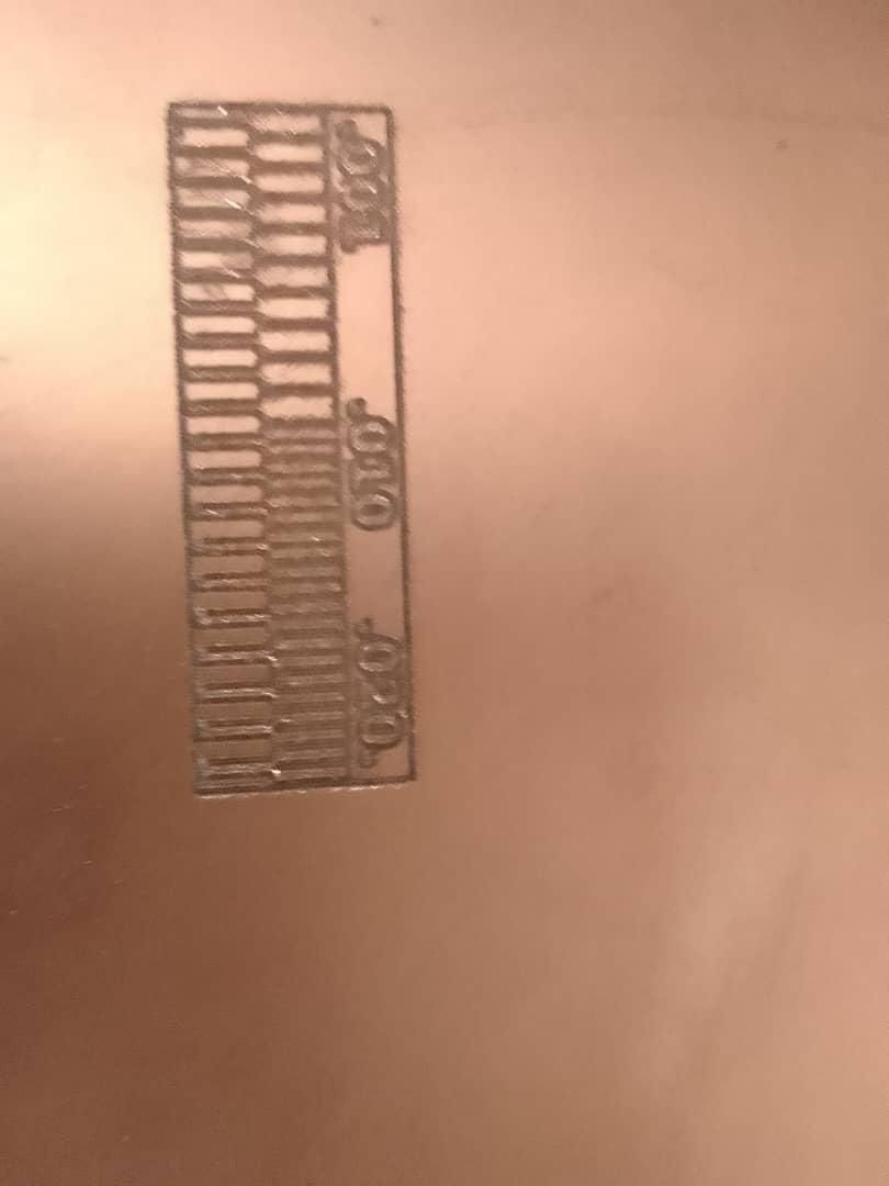
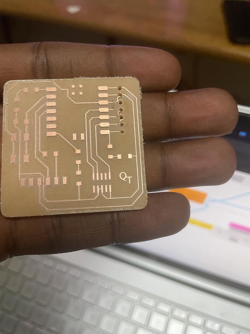
Final piece of PCB here.
PERSONAL WORK
To complete personal work, I used already prepared work in png format from images in the following link. click here to open the link. Thanks to the developers who prepared this work and made it open for use to try it out.
Traces image downloaded.
Drill image downloaded.

Outline image downloaded.

I followed the same steps as in the group work starting from fixing the sticker to the process of print on this stage for all the three images downloaded.
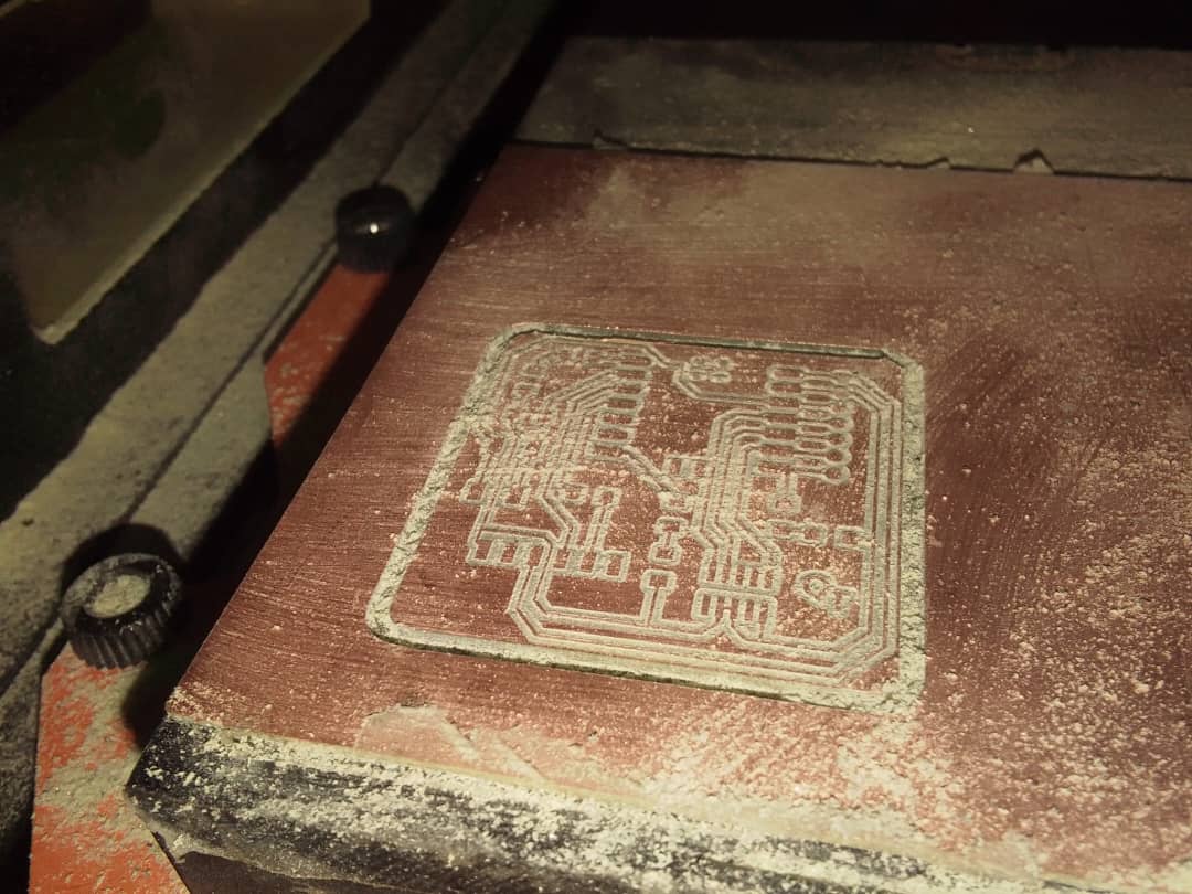
The PCB before outline to remove the piece.
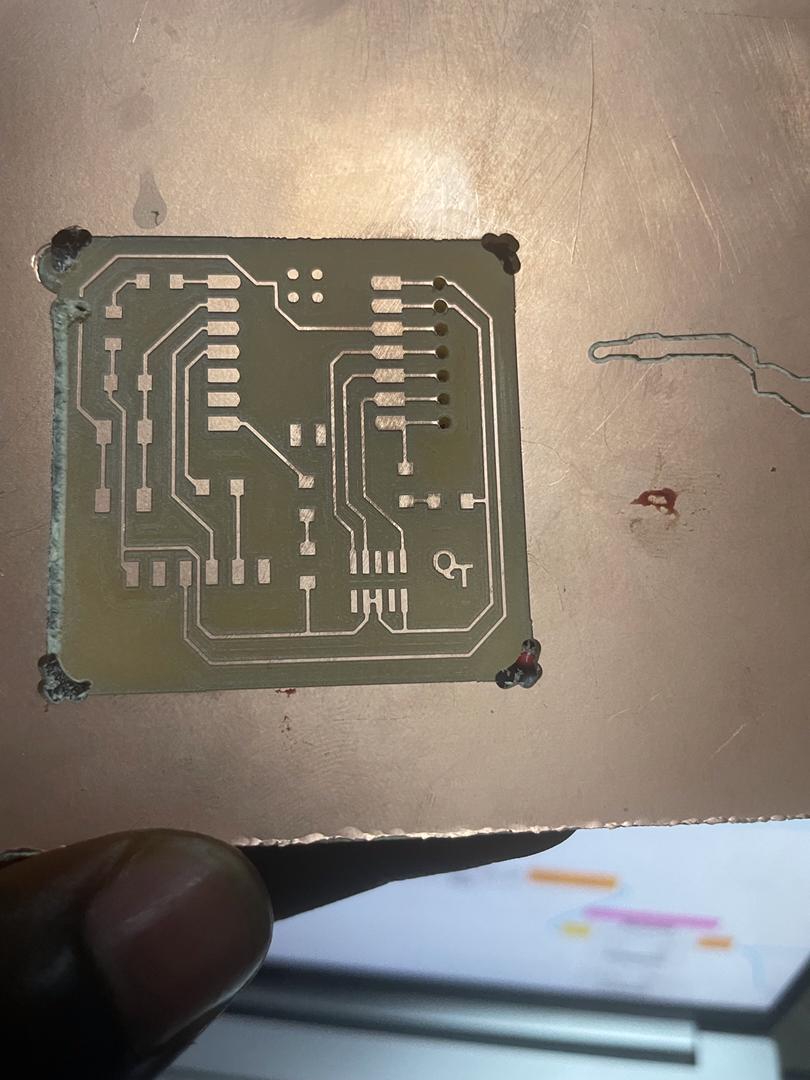
The final printed board.
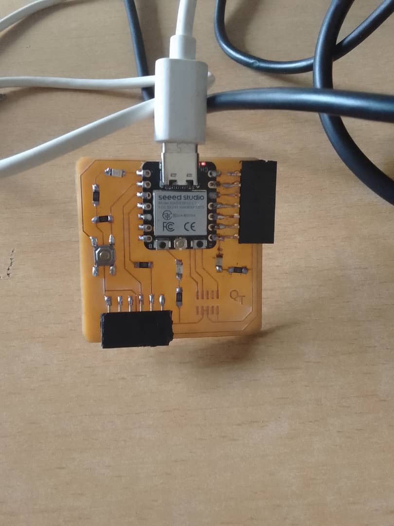
II. Microcontroller development board (Soldering and testing)
After PCB milling and printing we started soldering components on the PCB.
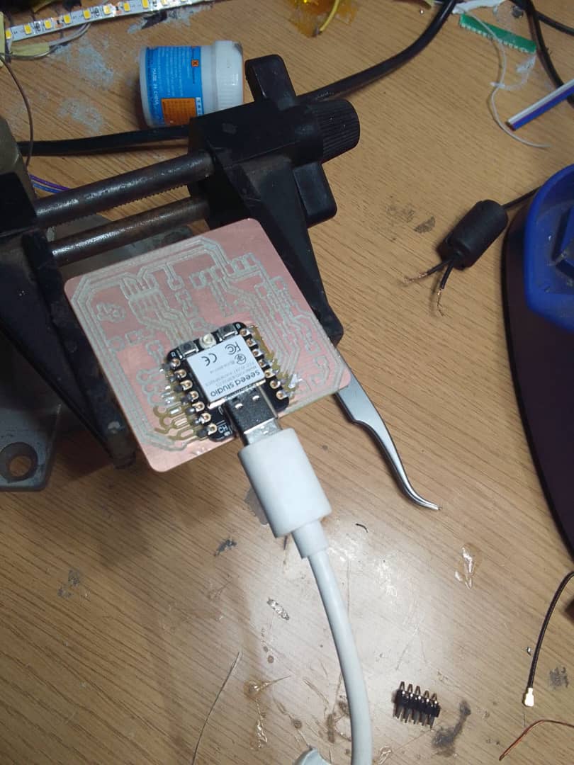
I tested the board and it was not ready in the port of the computer. We tried all the means with my fellow trainees and facilitator but could not work. By testing all the components, we found the microcontroller XIAO-ESP32-C3 not working. Then we decided to make a new board.
later I tested the pcb and it worked, i thought it was probaly some parts that we not soldered well.
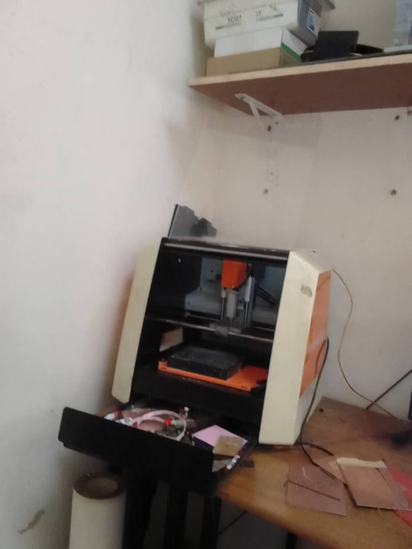
I started by printing a new PCB board and decided to test every step.
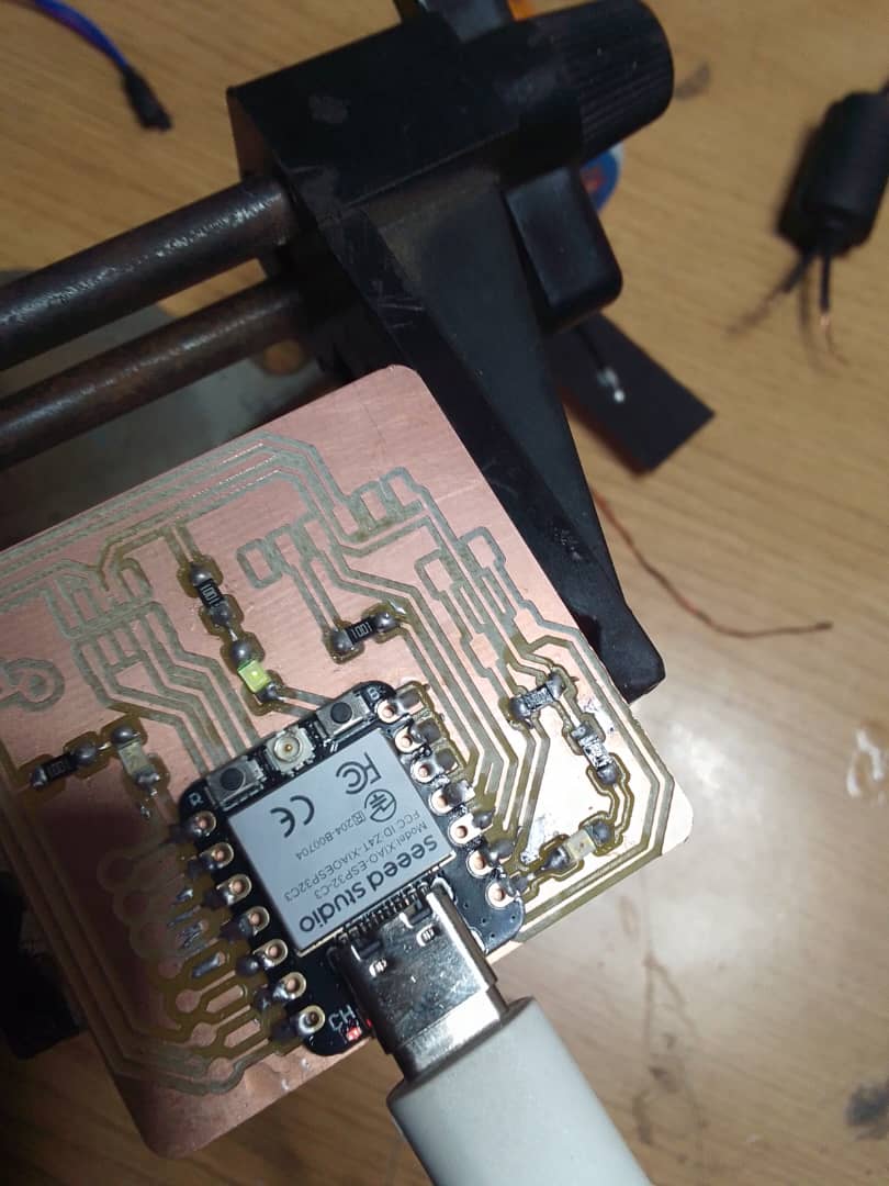
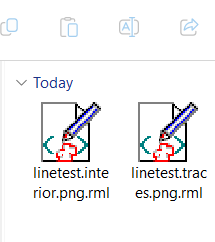
Now the New board works well. The file of traces of the working PCB is found with this document on below file list.