8. Electronics Design
Individual assignment
1. Desing
Finding the right software to kickstart the PCB design process was essential, and after careful consideration, I settled on KiCad as my tool of choice due to its reputation for robust functionality and versatility.
I had to install specific libraries to ensure that the components I intended to use would appear in the program.
The first thing i did was to open the option manage symbol libraries.
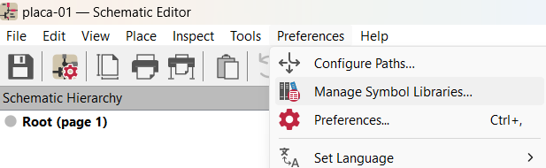
After the windows was open I add 2 files to the library using the +. This files were provided to us by our local evaluator.
Once that was done, I encountered no issues whatsoever in utilizing the software.
The first step was to design the circuit in KiCad, a software tool used for electronic design automation.
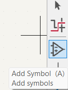
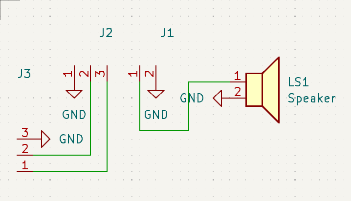
I used the add symbol button to add the components i used:
- Conn_PinSocket_1x02_P2.54mm_Horizontal_SMD
- Conn_PinSocket_1x03_P2.54mm_Horizontal_SMD
- GND
- Speaker
Then i drag every component until i was please with the position.
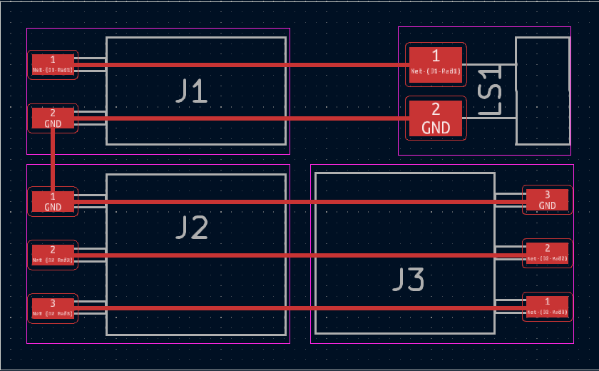
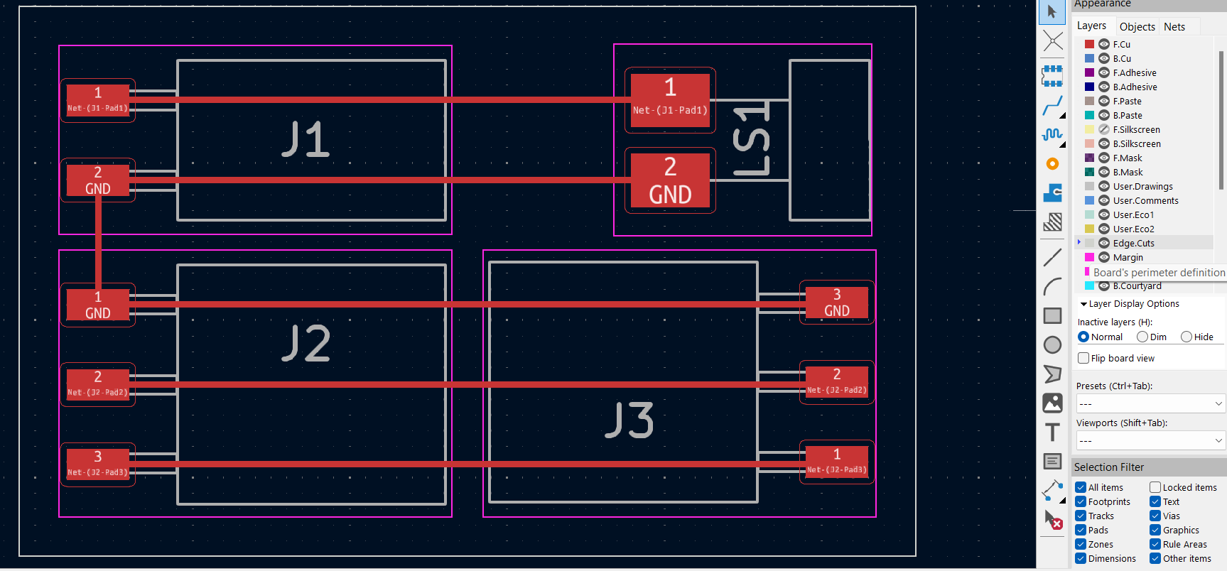
After this was done it was time to make the inner connections. So i change the layout to the PCB editor to start making the traces so every ground is connect.
I move some components to make it easy to aling some components. After i had the traces of the ground I started to trace the lines between the bridges and the speaker. Until i had something like this.
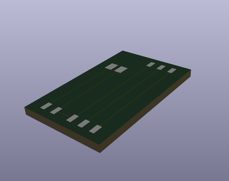
Using the 3D viewer tool it show me how the PCB will look.
I used the page MODS to import my pcb trace to the minimill. The parameters y used:
After setting up the Roland minimill, it start the process of cutting my pcb.

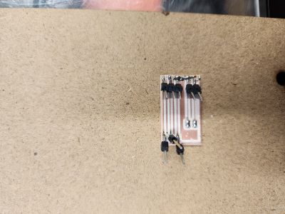
The final result.