Week 17 Project development
What tasks have been completed
Conducting a Field Visit During Social Service to Assess Needs and Identify Mechatronic Engineering Applications
Identify the need to detect lead in clay items and develop the concept for a device for this purpose.
Research the functioning of spectrophotometers and methods for performing lead detection tests.
Design a 3D model for a mechanism to analyze multiple samples.
Develop PCBs for connecting motors, an LCD, a photodiode, and an LED.
Integrate communication between these boards and develop the necessary software.
Research how to perform the test manually in a chemistry lab.
What tasks remain?
Final devive assembly :
Integrate all mechanical, electronic and software components into a functional prototype right now i already have it, but i need to put it pretty and less messy.
Compplete all the documentation
I need to finish 4 previous weeks, i only did the practice and physical tasks, but i had to make all the documentation, and also i plan to:
What has worked? what hasn't?

| CNC Structure | I was unable to obtain an LED that operates at a wavelength of 200 nm. |
| Integration of the boards and communication between them. | Adaptation of the OPT101 light sensor to a custom-designed board. |
| Sampling tests to detect copper using a standard solution. | |
| CNC programming. |
What questions need to be resolved?
Calibration Curve
Before finalizing this project, I need to perform a calibration curve by sampling approximately 20 samples. Here, I want to verify and compare the efficiency of absorbance against the university's spectrometer.
Cost-Benefit Analysis
- Conduct an economic analysis of the device, considering materials, assembly time, and potential mass production costs.
- Compare the costs with similar commercial devices.
Testing in Different Environments
- Evaluate the device under various environmental conditions (temperature, humidity) to ensure its robustness.
- Perform field tests with end users to gather feedback.
what will happen when?
By now i already presented on June 10th, i couldn't finish the documentation of my weeks but by that time i already had all the evidence, photos, PCBS, my final project.
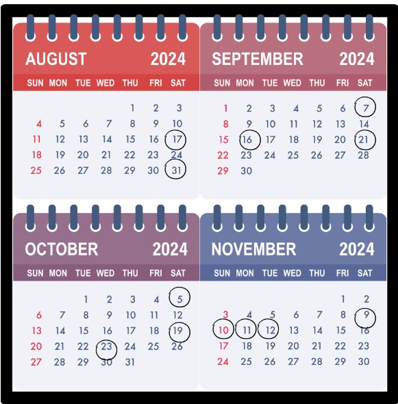
So i'm planning how to do it in a more efficient way to finisih by November 15th.

- August 17, 2024 : Finish documentation Week 8, electronics Design
- August 31, 2024 : Finish documentation Week 9, Mechanical Design, Machine Design
- September 7, 2024 : Mid Term Review
- September 16, 2024 : Input devices
- September 21, 2024 : Moulding and Casting
- October 5, 2024 : Output devices
- October 19, 2024 : Embedded Networking and Communications
- October 23, 2024 : Interface and Application Programming
- November 3, 2024 : Wildcard week
- November 9, 2024 : Applications and implications
- November 10, 2024 : Project development
- November 11, 2024 : Intellectual property
- November 12, 2024: Final project documentation
what have you learned?
What I learned from this experience in the Fab Lab is the great importance of time management. There were many tasks to complete for the Fab Academy that I thought would be quick, but I never imagined how time-consuming documenting everything would be. Along the way, I learned several methods to make the documentation process more efficient, such as recording myself in audio while working on a program or activity. This helped me easily recall how to detail each week and its activities. I also learned a lot about HTML and CSS to make my website a bit different while keeping it simple. I believe integrating so many aspects was challenging.
