Electronics design
This week I worked on electronics design. I liked learning about this tool, I remembered very basic physics things such as the use of resistors, power source, etc. It was a challenge to integrate things reviewed in previous weeks, apply what was done this week and have the vision in the design for the deliveries of the coming weeks.
Electronic design, also known as electronic engineering or electrical engineering, is a field of engineering focused on the design, development, and testing of electronic systems, devices, and components. It encompasses a wide range of applications, from small-scale integrated circuits to large-scale systems such as telecommunications networks and aerospace systems.
Electronic design involves the application of principles from physics, mathematics, and engineering to create electronic circuits and systems that perform specific functions. This process typically involves several stages:
Requirements Analysis:
Conceptual Design:
Developing high-level concepts and architectures for the electronic system based on the requirements analysis. This may involve selecting appropriate technologies, components, and design approaches. Detailed Design: Creating detailed designs of individual circuits, components, and subsystems within the electronic system. This includes selecting specific components, designing circuit layouts, and optimizing performance.Simulation and Analysis:
Using computer-aided design (CAD) tools to simulate the behavior of electronic circuits and systems, predict performance, and identify potential issues or areas for improvement.Prototyping:
Building physical prototypes of the electronic system to test and validate its functionality, performance, and reliability. This may involve breadboarding, soldering, and assembling electronic components.Testing and Verification:
Conducting thorough testing and verification of the electronic system to ensure that it meets the specified requirements and performs as intended. This may include functional testing, performance testing, environmental testing, and compliance testing.Iterative Design:
Iterating on the design based on test results, feedback, and changes in requirements. This may involve making adjustments to the design, refining prototypes, and retesting to achieve the desired outcome.Documentation and Manufacturing:
Documenting the design, including schematics, specifications, test results, and manufacturing instructions. Once the design is finalized, it may be handed off to manufacturing for mass production. Electronic design is a broad and interdisciplinary field that encompasses various sub-disciplines, including analog design, digital design, mixed-signal design, power electronics, RF and microwave engineering, embedded systems design, and more. It plays a crucial role in advancing technology and innovation in industries such as consumer electronics, telecommunications, automotive, healthcare, aerospace, and beyond. There are several programs used for electronic design and design automation (EDA). Some of the most popular include:Eagle (Autodesk Eagle):
Eagle is another widely used EDA software, especially in commercial and professional environments. Provides tools for schematic creation, PCB design, manufacturing file generation, and more. Eagle offers an intuitive user interface and a wide range of component libraries.Altium Designer:
Altium Designer is a complete electronic design software suite that includes tools for schematic, PCB design, simulation, library management, and much more. It is widely used in the industry and is known for its power and versatility, although it can be expensive to license.OrCAD:
OrCAD is an EDA software suite developed by Cadence Design Systems. It offers tools for schematics, PCB design, circuit simulation, signal analysis, and more. OrCAD is widely used in the electronics industry and is known for its robustness and functionality.DipTrace:
DipTrace is a cost-effective alternative to KiCad and other commercial EDA programs. It offers tools for schematics, PCB layout, track routing, manufacturing file generation, and more. DipTrace is known for its ease of use and active community of users.DesignSpark PCB:
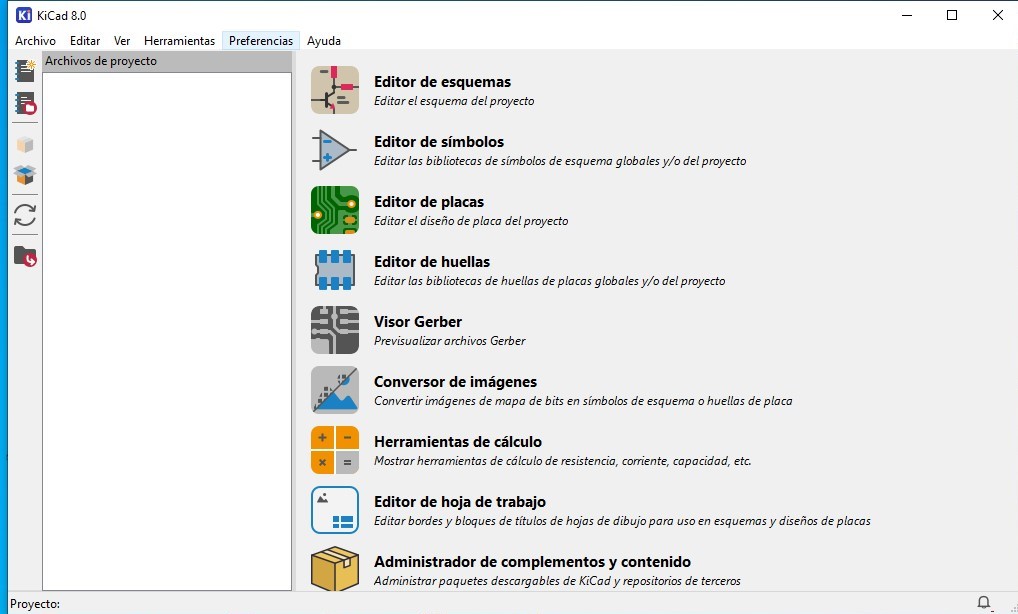
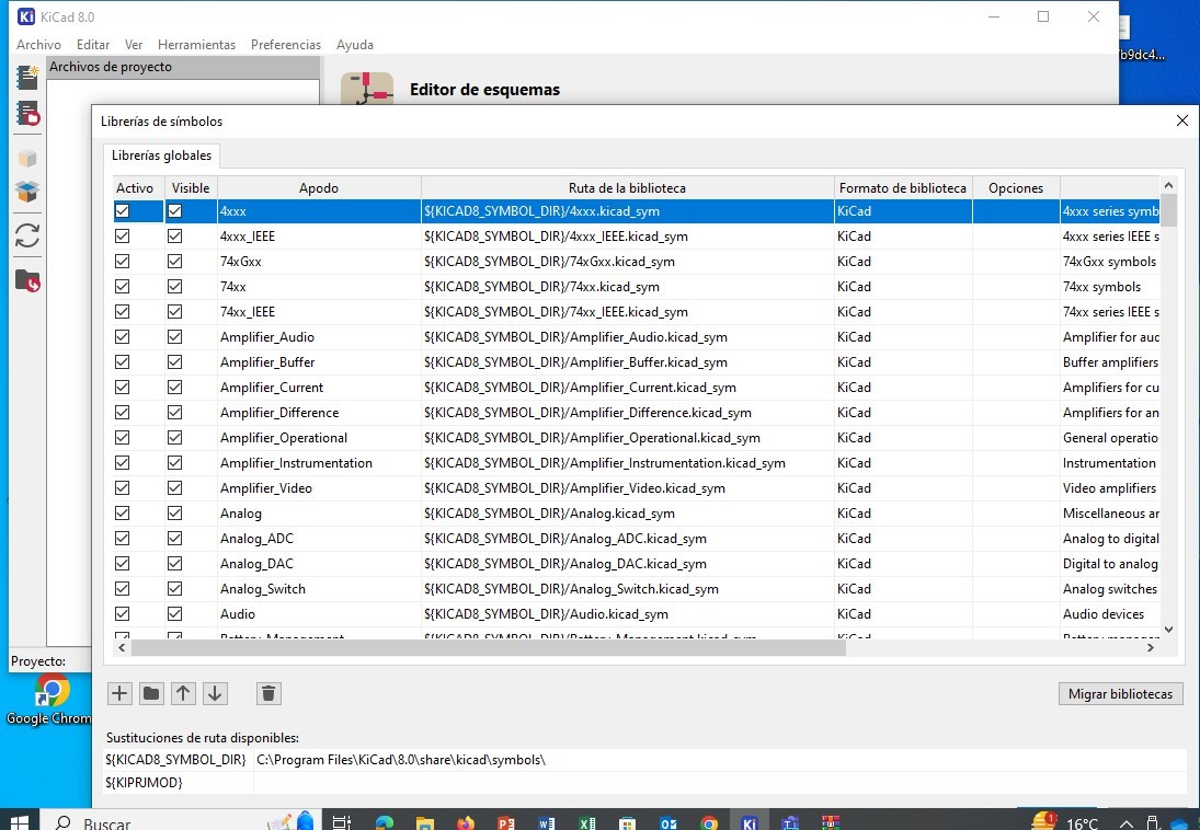
DesignSpark PCB is a free EDA software developed by RS Components. Offers tools for schematics, PCB design, component library creation, and more. DesignSpark PCB is popular with amateur designers and professionals looking for a free, easy-to-use solution.KiCad
is an open-source software suite used for electronic design automation (EDA). It provides tools for schematic capture, printed circuit board (PCB) layout, and component footprint creation. KiCad is popular among hobbyists, students, and professionals for designing electronic circuits and PCBs. Key features of KiCad include:Stages of the process of lectronics design
It was a very complicated week. I did this assessing in different stages: Stage 1: Idea Stage 2: Dessign ussing KiCad Stage 3: Cutting and engraving Stage 4: Assembly Stage 5: Check
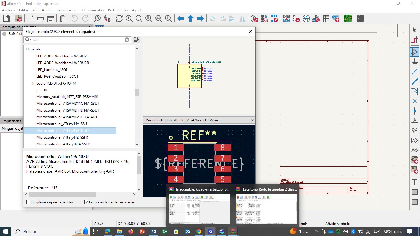
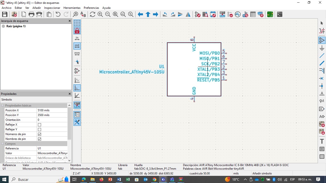
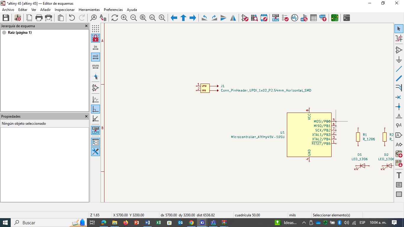
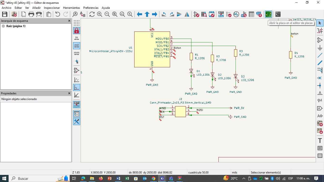
Stage 1: Idea & design Imagining the object to make this week was difficult The idea was to design a circuit that could have interaction to turn on, turn off or coordinate the turning on of three LEDs using a button. ee XIAO-RP2040, I want to make a design to place three LEDs, a button and thinking about future weeks I want it to be useful to be able to put a humidity and temperature sensor. I also want the humidity and temperature sensor to be part of my 3D printer for my final project. I searched and found that DHT22 sensor can be a good option and made this design.
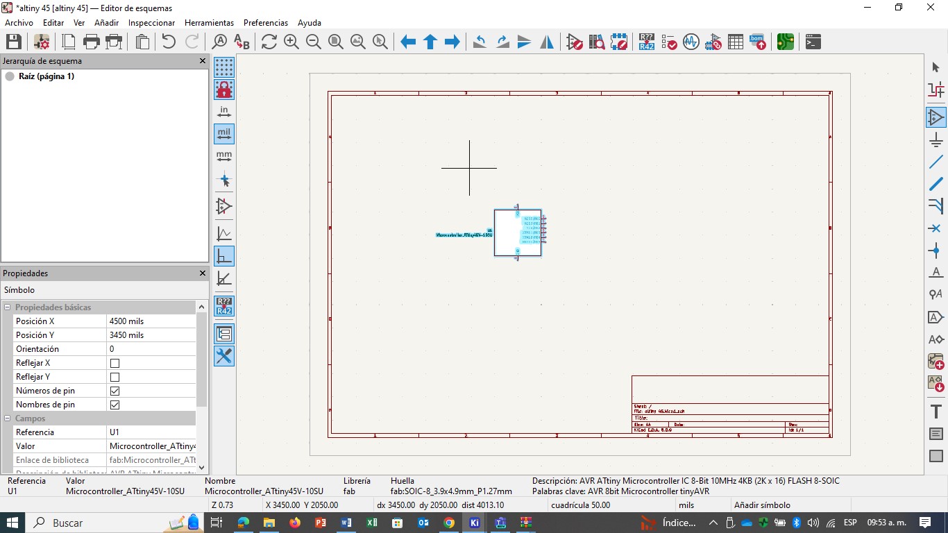
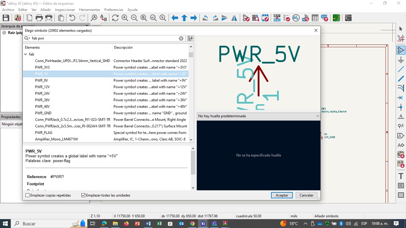
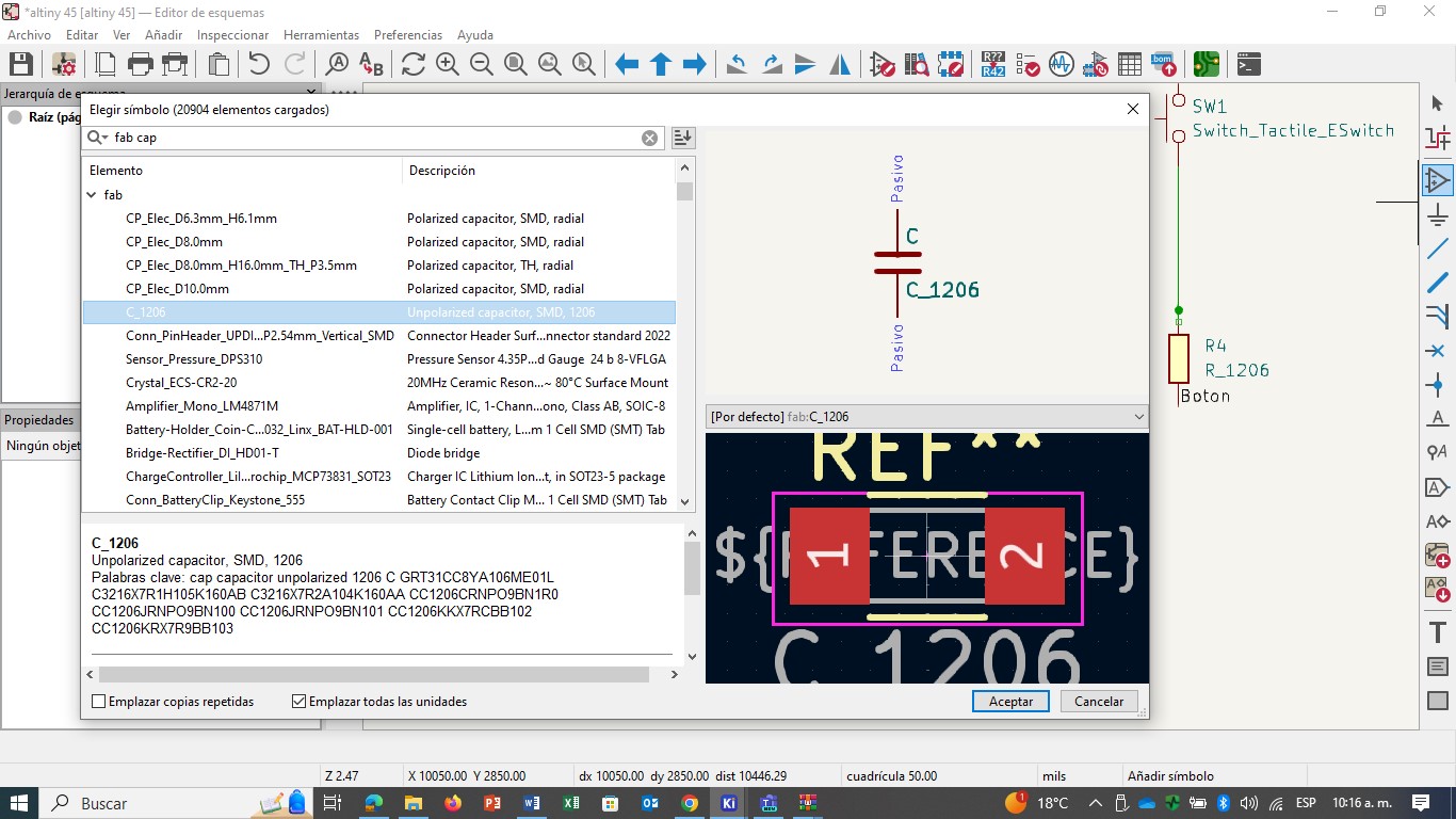
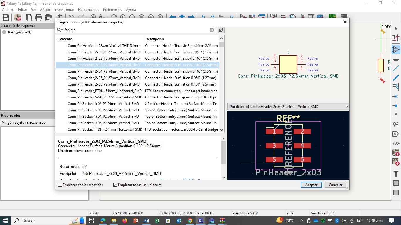
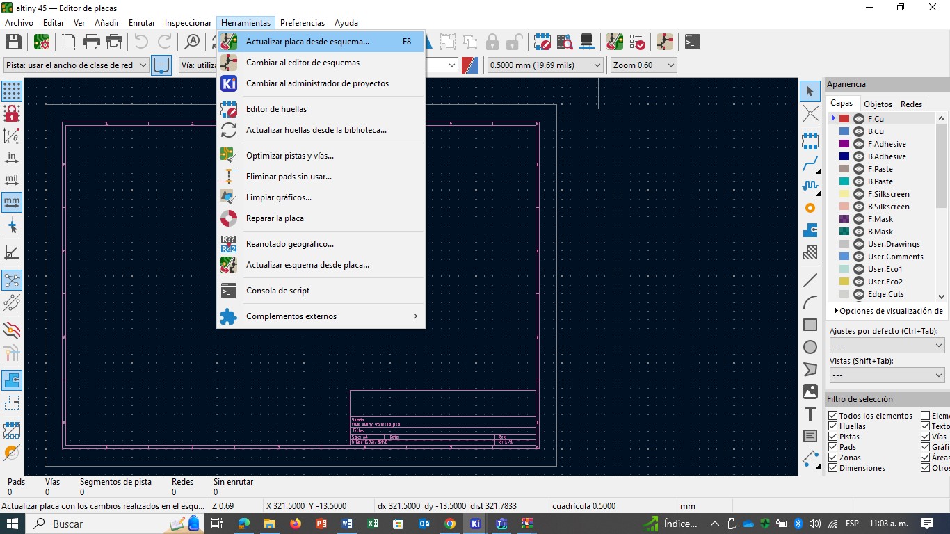
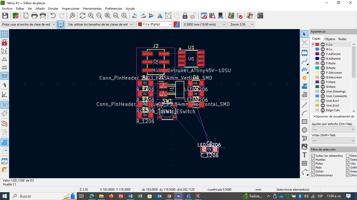
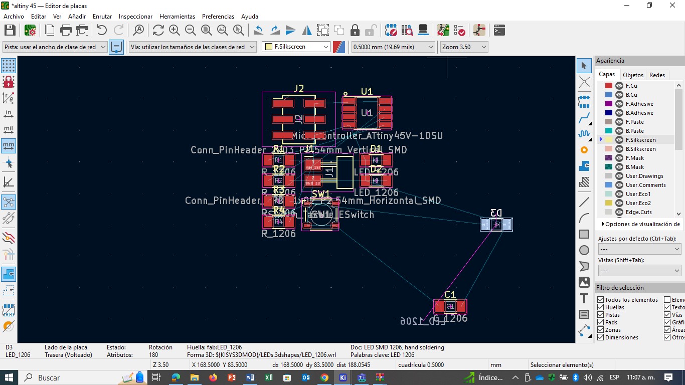
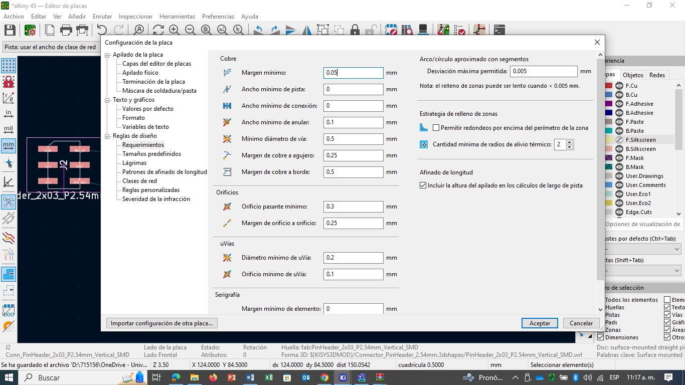
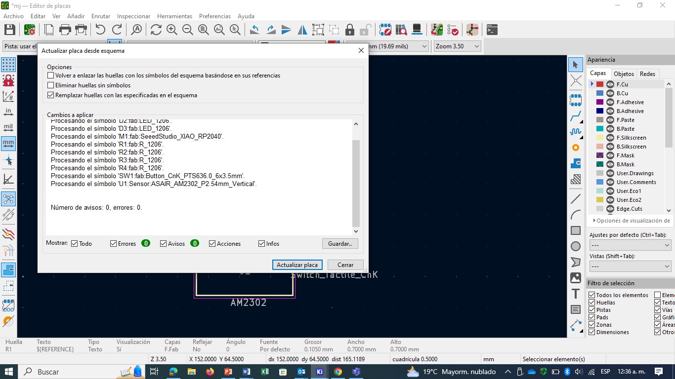
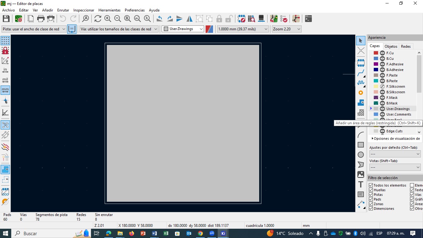
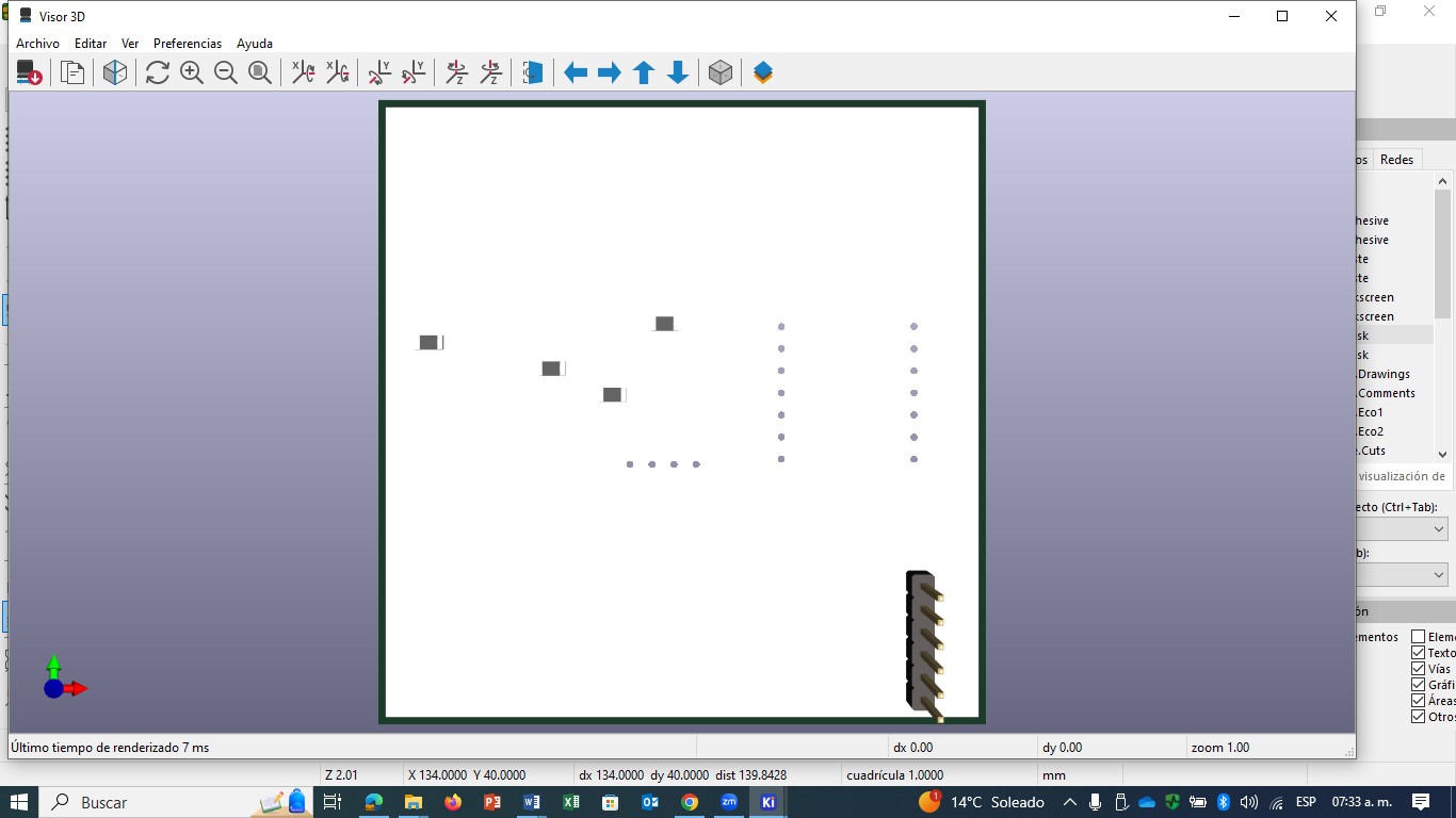
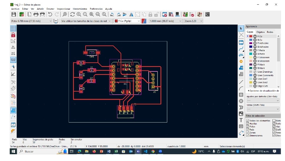
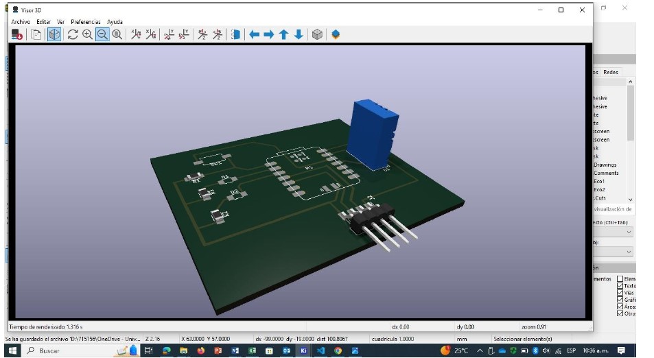
Stage 2: Dessign ussing KiCad

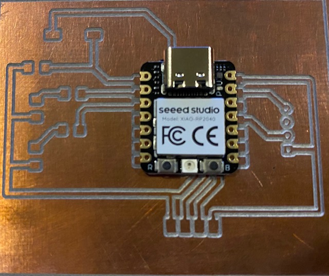
Stage 3: Cutting and engraving
To cut and engrave the designed circuit, the ROLAND SRM-20 PCB Milling mini was used. To remember the use of the machine you can review the topic in the Follow link Electronics Production-Fablab Puela
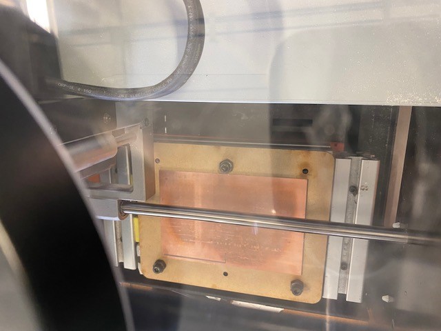
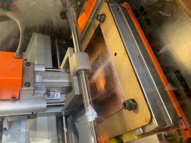
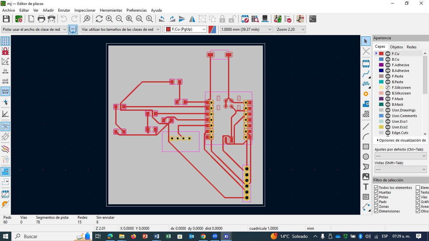
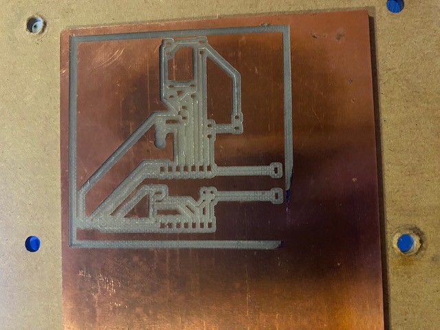
The design was not correctly engraved or cut, and there were errors in the design due to the thickness of the tracks and connections. Therefore, with the same instructions, a new design was made that is presented in the images.
Stage 4: Assembly
Stage 5: Check
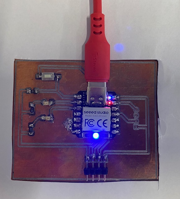
It's not ready yet
Conclusion
It was a very active week, he use of KiCad did not seem so complicated to me, once the functions and necessary components are clear, the design is quite intuitive using KiCad. This has tools to detect errors easily. I had problems installing the board to cut and etch the circuit I designed. Unfortunately, I could not remove the inclusion and this did not allow the tracks to be recorded well, so they are not distinguishable. It is necessary to review the design and try to re-record the circuit.