8. Electronics Production
This week's assignment was to design A development board to program and communicate with a microcontroller
Group assignment
All the documentation about the equipment realated to electronics production can be found on Ibero Pueblas week 8 group page. There you can found the tipe of equipment we use and clear instruction on how to use it. Fablab Puebla week 8
Designing my PCB
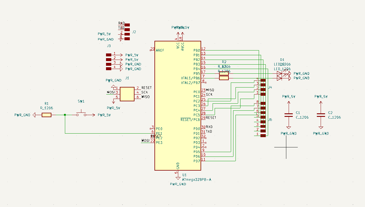
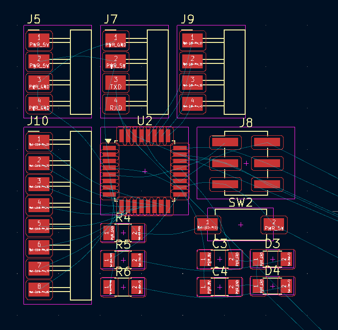
I used KiCad to design my PCB, the first step to making my PCB was to choose the components of my board. For my microcontroller, I used the ATMEGA328PB-A, all microcontrollers available in Ibero Puebla can be found on our Fab Academy page in week 6. Fablab Puebla. I decided to recreate an Arduino board in order to communicate with other boards for future projects like next week's output devices. In order to get started I first selected the components for my PCB in the schematic editor. There are libraries with a wide variety of components.

To recreate an Arduino board First I looked up the components of the ATMEGA328PB-A.
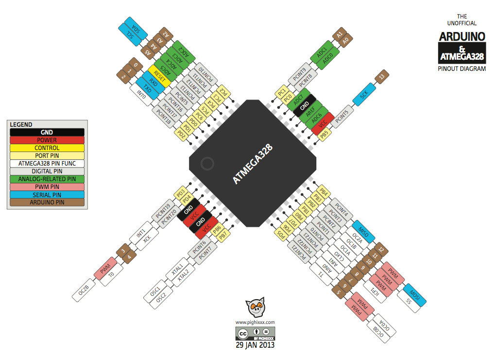
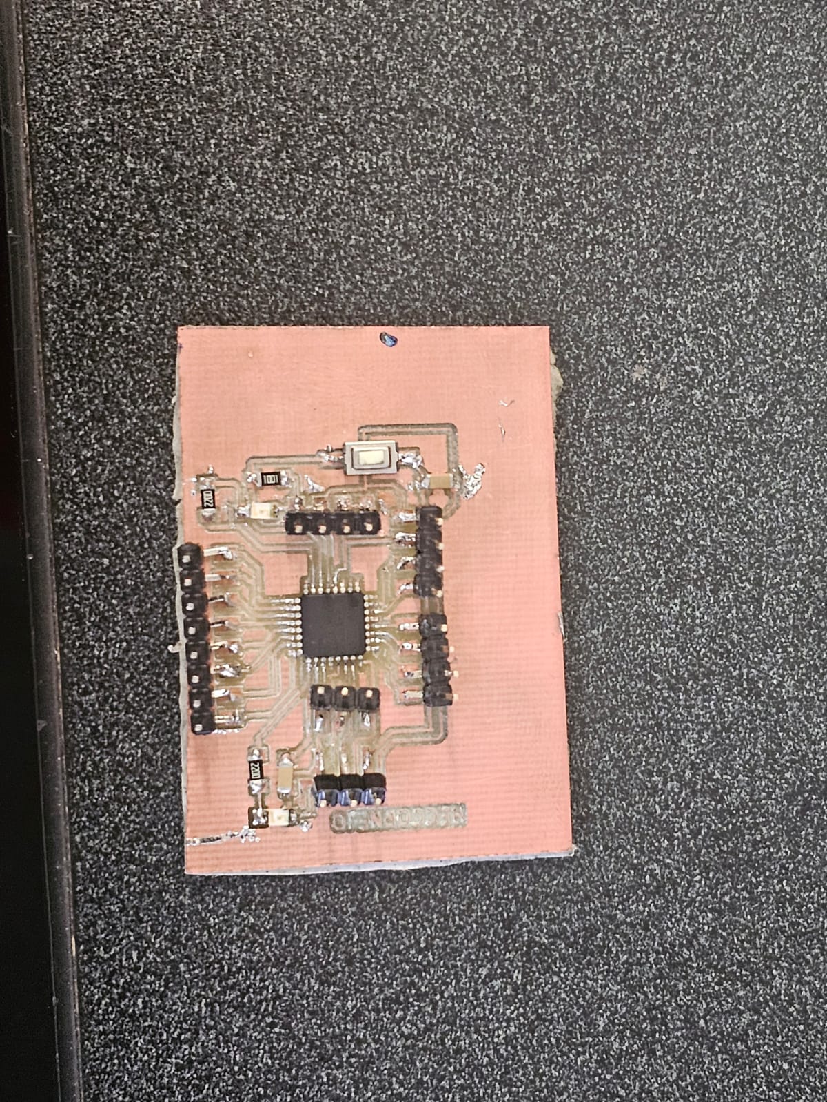
For my components I used 26 pins for digital exits, RXD and TXD signals, and programming pins, RXD and TXD signals, and programming pins, 2 LEDs, 1 button, 2 220 resistors, 1 1k resistor, and 2 capacitors.Following the ATMEGA328PB-A schematics I made the connections to my components.
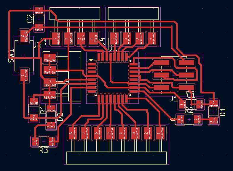
Once I had my connections it was time to arrange my PCB. To do this I used the PCB editor. There I uploaded my microcontroller and components to the PCB editor by selecting the tool's in the top menu and the updating my PCB frrom my Schematics.
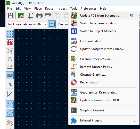
First, all of the components in the Schematic editor appear disarranged with only some indications of what components need to be interconnected. Arranging the components was probably one of the most time--consuming activities of this week's assignment.
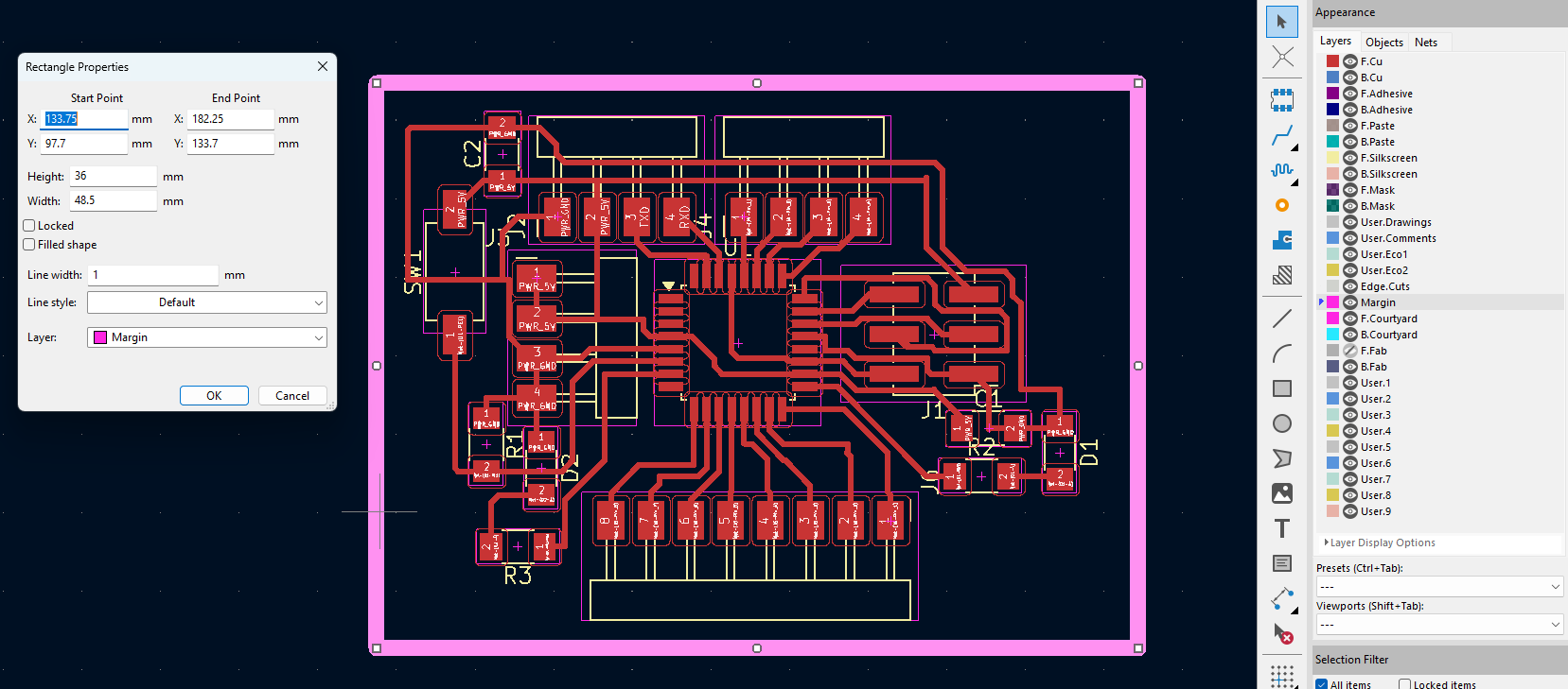
Then I added a margin using the appearance menu, selected the margin option, and then I added a square around my PCB design, after that, I gave my margin a width of 1 millimeter.
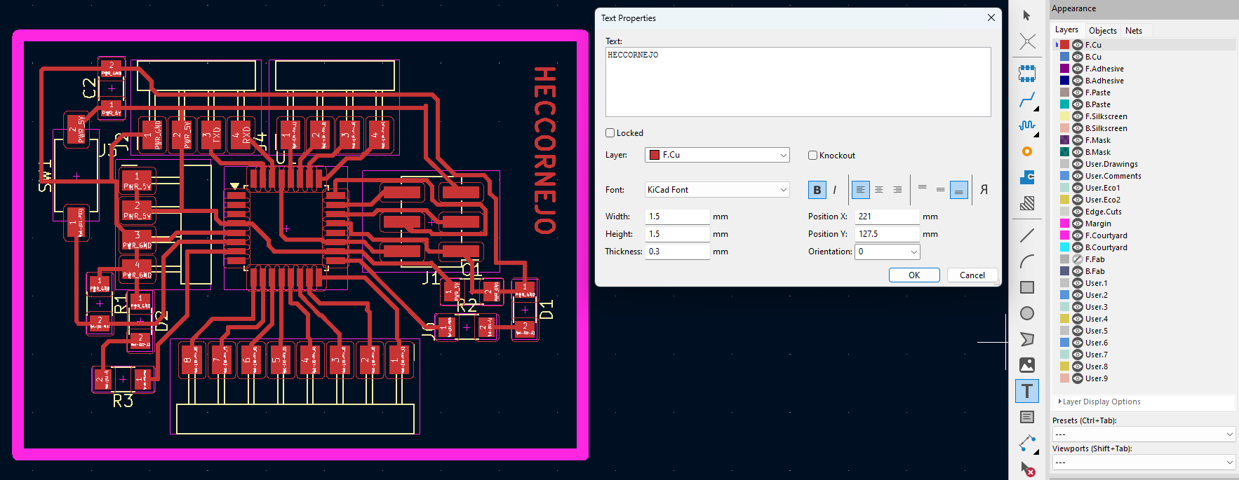
Finally, I added an engraving in my PCB by selecting the Text Properties tool and writing what I wanted engraved on my board.
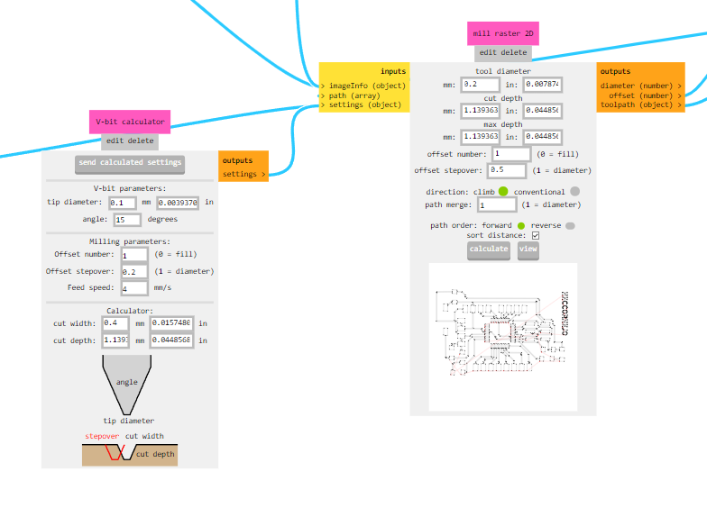
Once I was happy with the design of my PCB I exported it as an SVG file. Then I used Modes CE to generate the code for the Mini-mill. I opened the Roland Monofab PCB program.
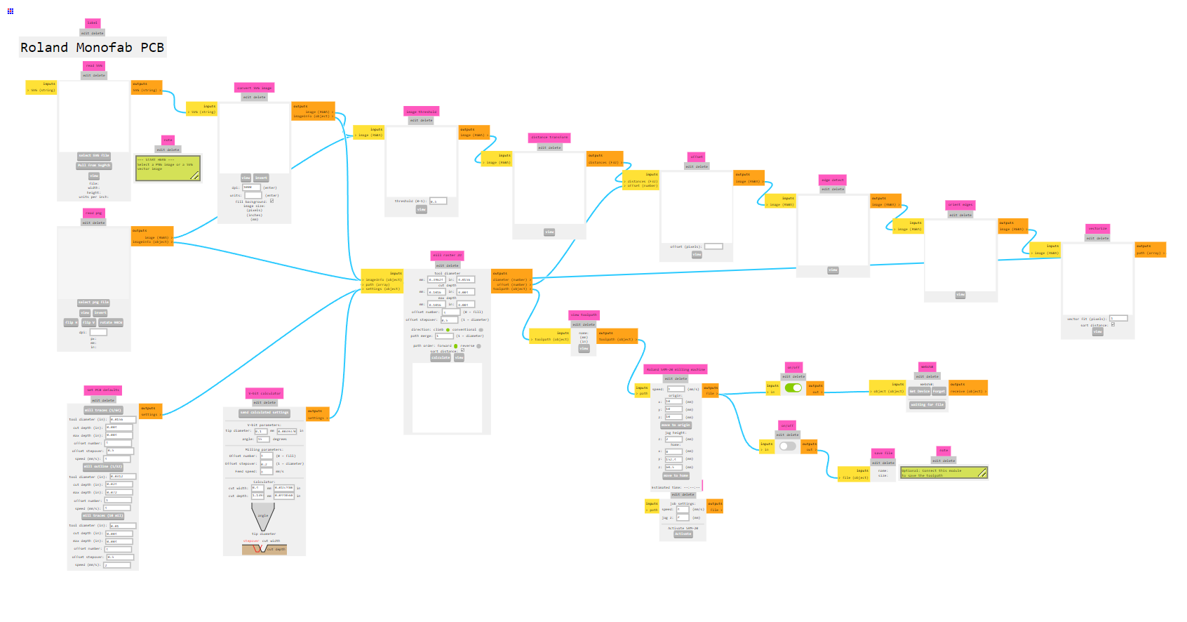
After opening my SVG file in Modes I made some modifications to the V--bit calculator and the mill rate 2D.
Engraving and Cutting
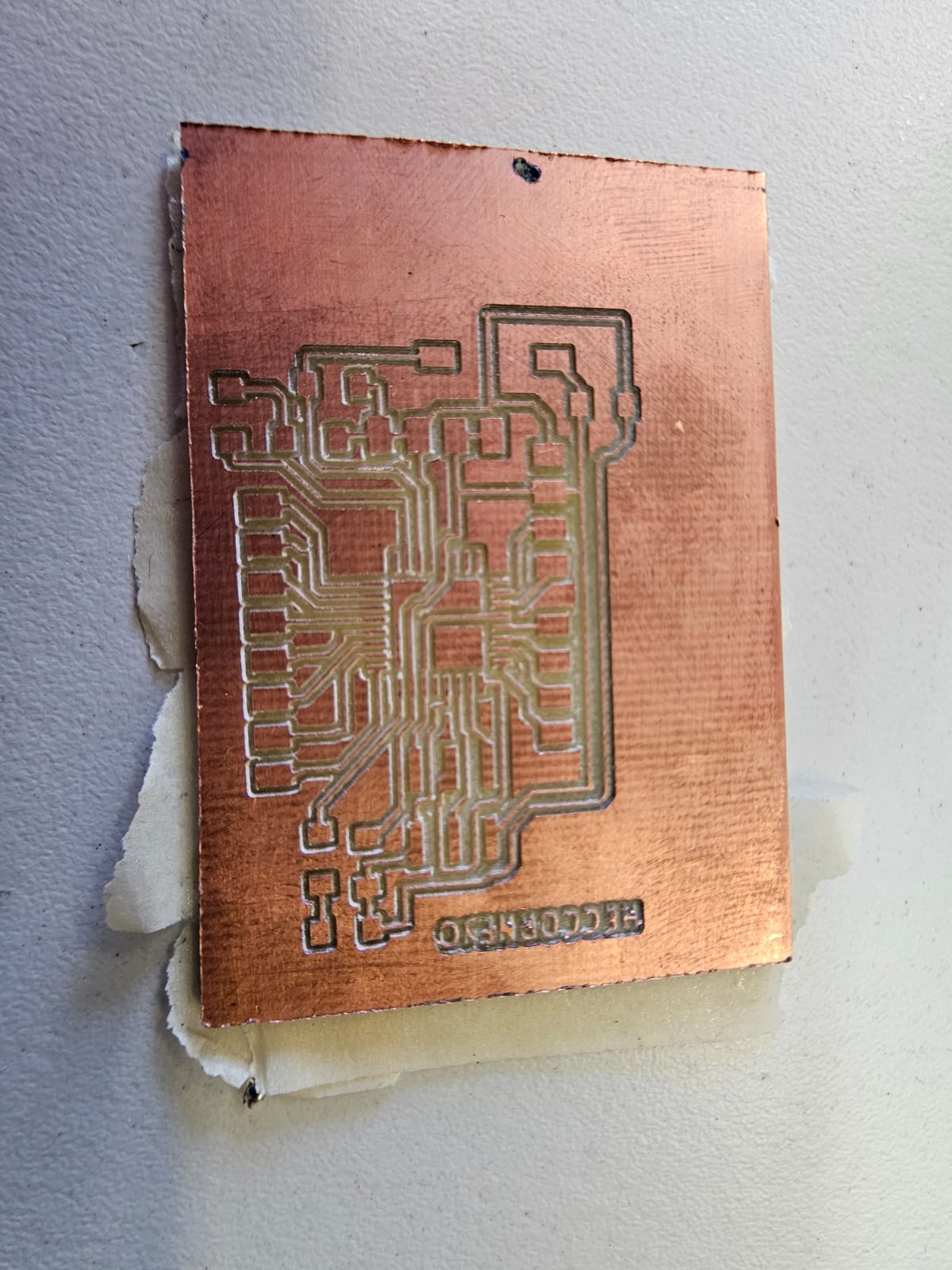
I used the SRM-20 to engrave and cut my PCB, the software is very user-friendly and self-explanatory. I selected an origin in x and y first, then I manually lowered the tool until it was touching the plate and there I selected my origin for Z. Once that was done I just started my cuts.
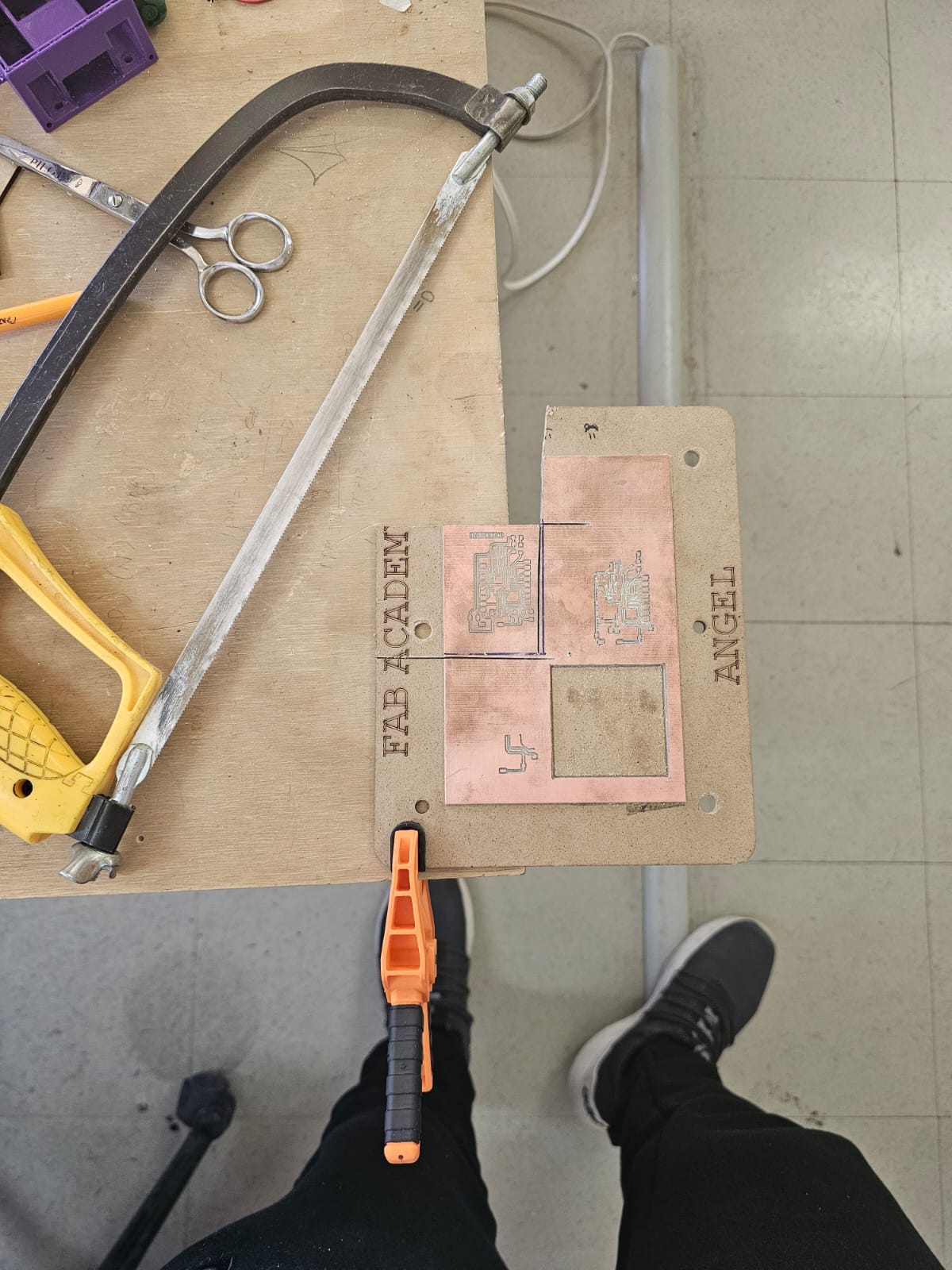
One problem I had was that after the engraving my origins got deleted so I had trouble trying to set up new ones to cut my PCB. After some tests and trying to align again my origins, I decided to cut my PCB by hand using a saw.
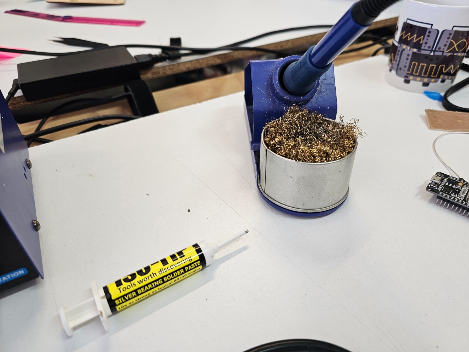
Soldering
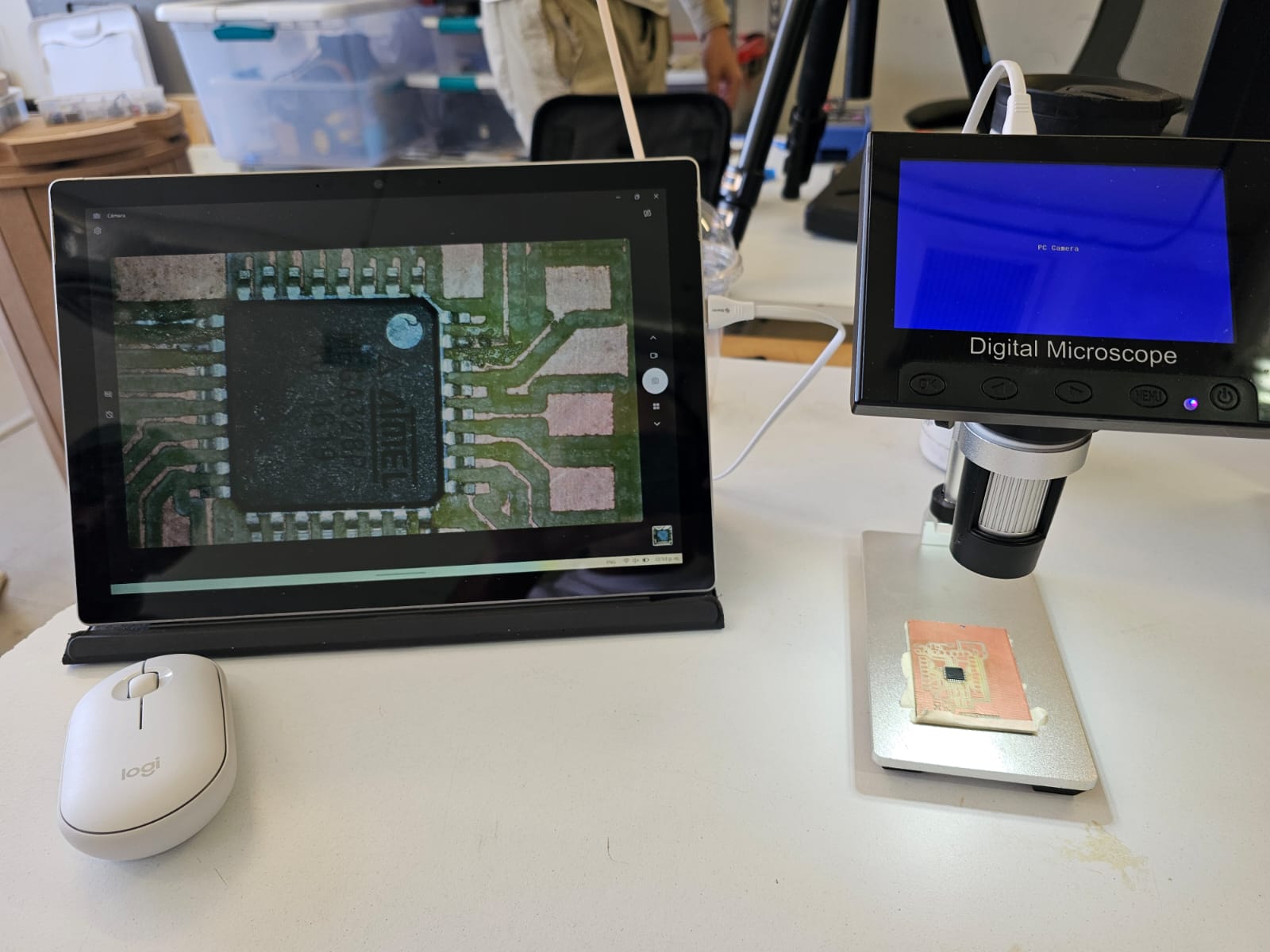
Soldering the ATmega was a challenge, I had never soldered anything that small before. First I solder the ATmega, to do so I used liquid tin and a digital microscope. It took me an hour to solder the ATmega.
After that I just soldered the rest of the components
Final result