WEEK 8
ELECTRONICS DESIGN
For this week, I designed my first PCB from scratch! It was indeed a great challenge, but I was very excited about what I could accomplish. I knew I wanted to try using Neopixels and also start experimenting with some things that would work for my final project. So, keep reading if you want to see the final result.
Something important this week was the introduction we had to the electronics part during the group assignment, which you can see here. As an industrial designer in university, I hadn't received training in this area, and even though the basic concepts can be easy to understand, it felt like dusting off my high school physics classes. Below, I'll provide a summary of these concepts in an easy and straightforward manner. And if, like me, physics doesn't always treat you kindly, try using technology to your advantage, like Chat GPT, to better understand the topics.
-
Electric Current: Imagine that electrons are like tiny balls that can move along a path made of wires. Electric current is like the flow of these little balls along the path.
-
Voltage: Think of voltage as the force that pushes these balls to move along the path. The higher the voltage, the faster the balls will move.
-
Resistance: Sometimes, the path along which the balls travel can be narrow or difficult to pass through. Resistance is like obstacles on that path that make the balls have to exert more effort to keep going.
-
Ohm's Law: This law tells us how voltaje (V), current (I), and resistance (R) are related to each other. It helps us understand how the balls behave on the path.
-
Voltage (V) = Current (I) × Resistance (R): This formula tells us that if there are many obstacles on the path (resistance), the balls will have to exert more effort to advance. Therefore, the voltage needed for the balls to overcome these obstacles is equal to the amount of balls (current) multiplied by the difficulty of the path (resistance). In other words, if we increase the current or the resistance, the voltage will also increase proportionally.
-
Current (I) = Voltage (V) ÷ Resistance (R): Continuing with the analogy, if we know the force (voltage) pushing the balls and the difficulty of the path (resistance), we can calculate how many balls will pass per second. This is done by dividing the voltage by the resistance. If the voltage is high or the resistance is low, there will be more balls (current) flowing. So, if we increase the voltage or reduce the resistance, the current will increase.
-
Resistance (R) = Voltage (V) ÷ Current (I): Lastly, if we know the force (voltage) pushing the balls and the number of balls passing per second (current), we can determine how difficult the path is. This is calculated by dividing the voltage by the current. If the voltage is high and the current is low, the apparent resistance of the path will be high, meaning that the balls will encounter more difficulty in advancing.
-
Electric Circuit: It's like a set of interconnected blocks. The blocks are electrical components like resistors, diodes, and lights, and they are connected by paths (the wires) along which the balls can travel.
-
Basic Components: These are like puzzle pieces used to build interesting things in the electric circuit. For example, resistors are like small obstacles that control the flow of the balls.
-
Analog and Digital Circuits: Analog circuits are like drawings that can have many colors mixed together, while digital circuits are like drawings made only with solid blocks of colors, one next to the other.
-
Signals: Imagine sending messages using little lights. Sometimes, the lights can shine dim or bright, or they can blink fast or slow. These are different signals that can send different messages.
-
Amplification and Attenuation: It's like when you use a megaphone to make your voice louder, that's amplification. And when you lower the volume of the music, that's attenuation.
-
Power: Power is like how fast you can do work. In our electrical world, it's how quickly we can use electricity to do things like light up a bulb or run a motor. It's like the strength of the flow of the balls along the path.
-
Boolean Logic: It's like a game with very simple rules. If you have two switches and both are turned on, then the light turns on! It's a fun game of turning things on and off.
Also, I'll share the basic symbols that need to be known to make electronic circuits.
Components
| NAME | SYMBOL | DESCRIPTION |
|---|---|---|
| Resistor |
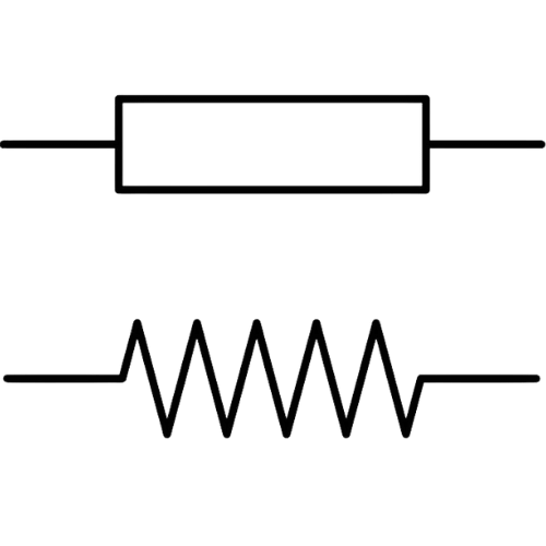
|
It's a component that reduces the flow of electrical current in a circuit. It's used to control the amount of current passing through a specific part of the circuit. |
| Capacitor |
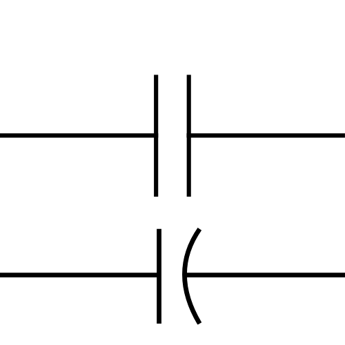
|
Stores energy in the form of electric charge. It acts like a temporary "battery" in the circuit, releasing or absorbing energy as needed. |
| Diode |

|
Allows electrical current to flow in only one direction. It works like a valve that lets current pass in one direction and blocks flow in the other. |
| LED |
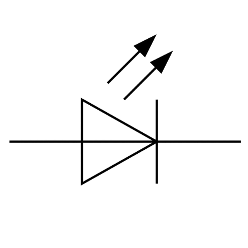
|
Similar to a regular diode, but it emits light when current passes through it. It's commonly used to indicate the status of a circuit or to illuminate devices. |
| Transistor |
|
Acts as a switch or amplifier of electrical signals. It can control the flow of current between two of its terminals based on the current or voltage applied to a third terminal. |
| Power Supply |
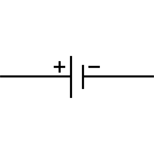
|
It's the source of electrical power for the circuit. It can be a battery, a power adapter, or another electrical power source. |
| Switch |
|
Opens or closes the circuit, allowing or interrupting the flow of electrical current. It's like a light switch that turns the light on or off. |
| Coil/Inductor |
|
Stores energy in the form of a magnetic field when electrical current passes through it. It's used in circuits to filter signals or to control electrical current. |
| Ground |

|
It's the common reference point in an electrical circuit. It's used as a zero-voltage reference and as a way to dissipate excess electrical current. |
LET'S START DESIGNING A PCB!
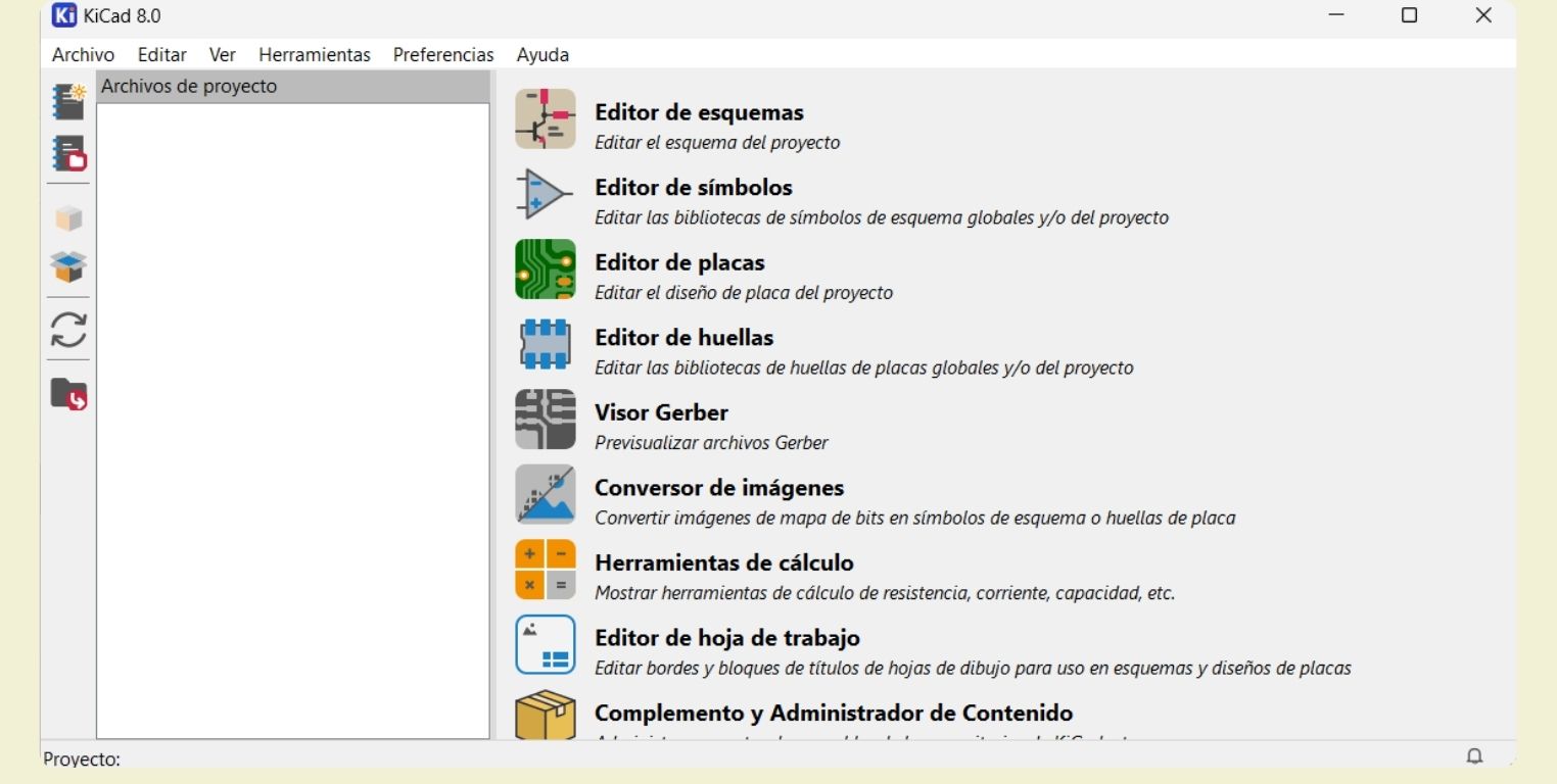
For the design of a PCB to be manufactured, it is necessary to use special software that we can trust for its fabrication. There are many currently available, but this time my instructors recommended KiCad.
 KiCad
is an electronic design automation (EDA) software that provides tools for schematic design, circuit
simulation, PCB routing, and manufacturing file generation.
KiCad
is an electronic design automation (EDA) software that provides tools for schematic design, circuit
simulation, PCB routing, and manufacturing file generation.
This is an overview of what you can see once the program is opened.
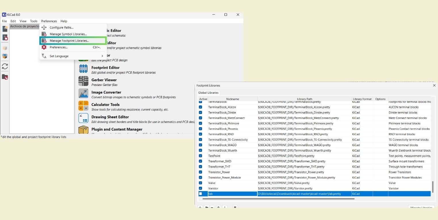
The first step was to install the libraries with the Fab components. In the "Preferences" menu, I clicked on "Manage Symbol Libraries...", and in a new "Library path" called "Fab" I added the "fab_kicad_sym" file by clicking on the folder.
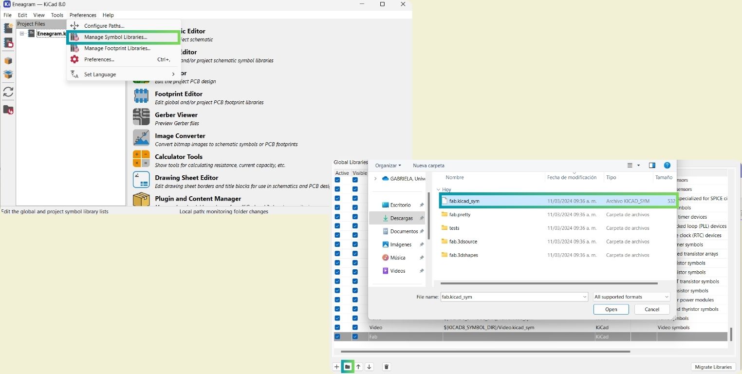
Then I went back to the beginning, and within the "Preferences" menu, in "Manage Footprint Libraries...", I added the "fab.pretty" file as I did with the previous one.
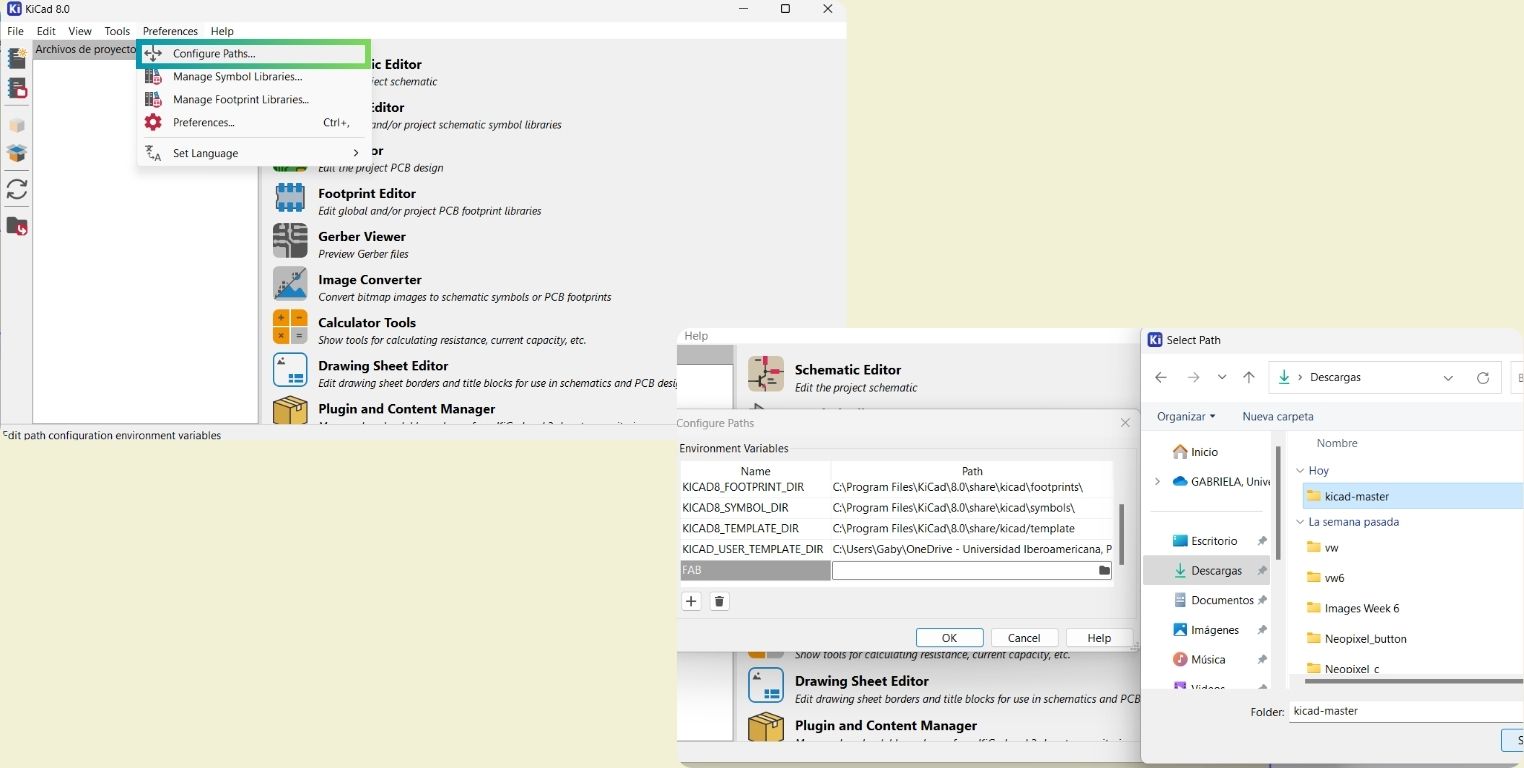
In "Configure Paths", I created a new variable called "FAB" and added the "kicad-master" folder to finish installing the libraries.
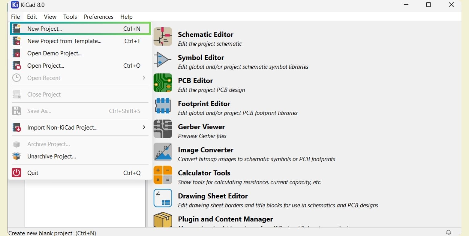
Within the "file" menu, I created a new project, and named it "Eneagram".
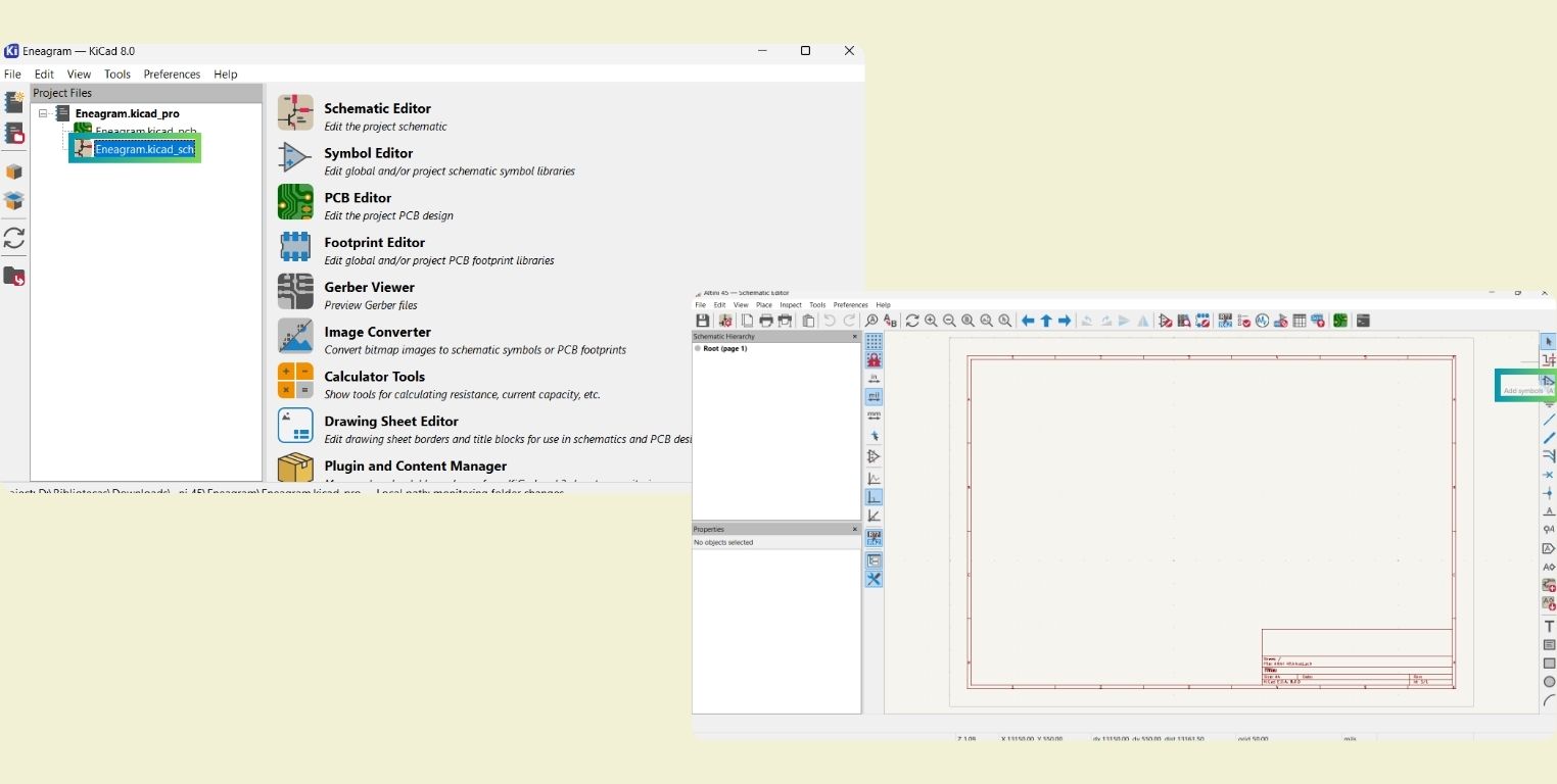
Schematic
From this new project, I selected the "Schematic Editor". To start, it is necessary to add the symbols of the components that will be used by clicking on the third symbol in the menu on the left.
Next to the magnifying glass, you can search for the component to make it faster. Once selected, the measurements appear at the bottom, and a link to the component's datasheet, which in the case of the Neopixel is necessary to know how it is connected, as each input and output is different. On the upper right side, you can see the symbol, and on the bottom side, you can see the footprint with which the PCB would be made.
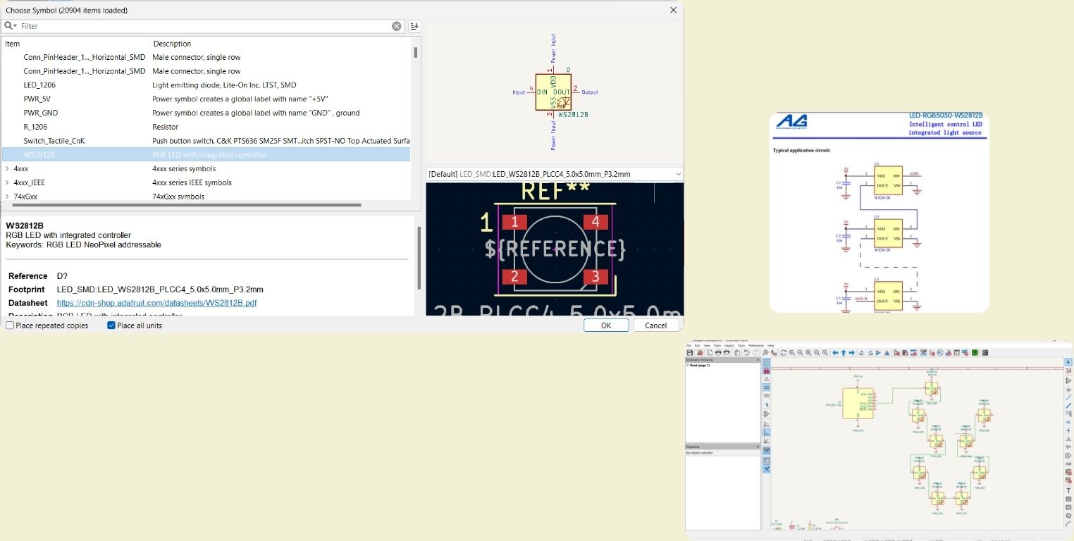
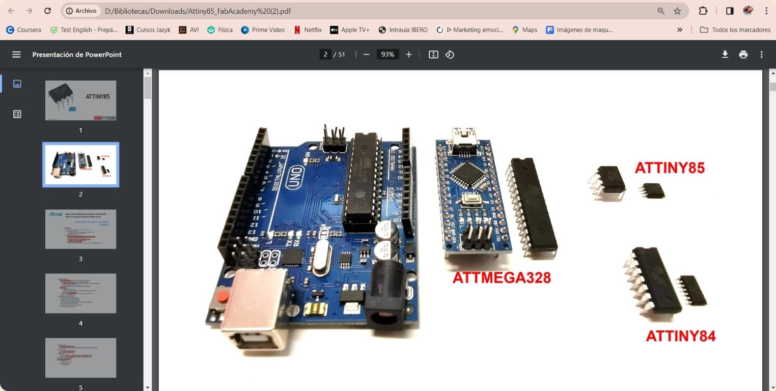
For this delivery, I worked with an ATTiny 45 microcontroller, the diagram says 85, but in reality, the footprint size is the same for both. According to the diagram I was using, I named it "MOSI/SDA, MISO, and SCK/SCL" on the corresponding pins of the ATTiny 45/85 microcontroller.
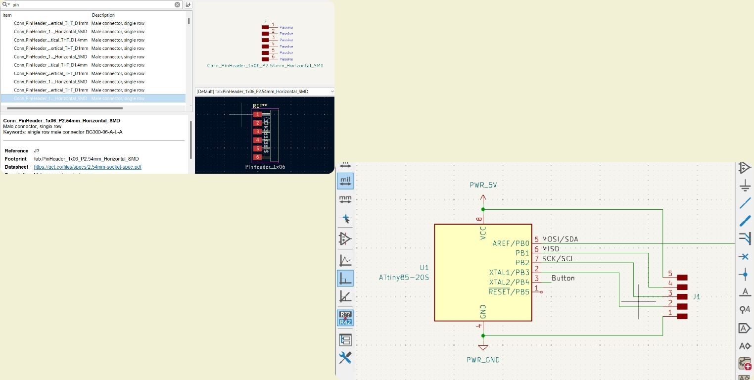
I also added 6 pins and connected them to the microcontroller. It is advisable to have several pins to be able to connect more things, especially if you also consider that the ATtiny has to be connected through these to an external programmer to be able to save codes and test its functionality.
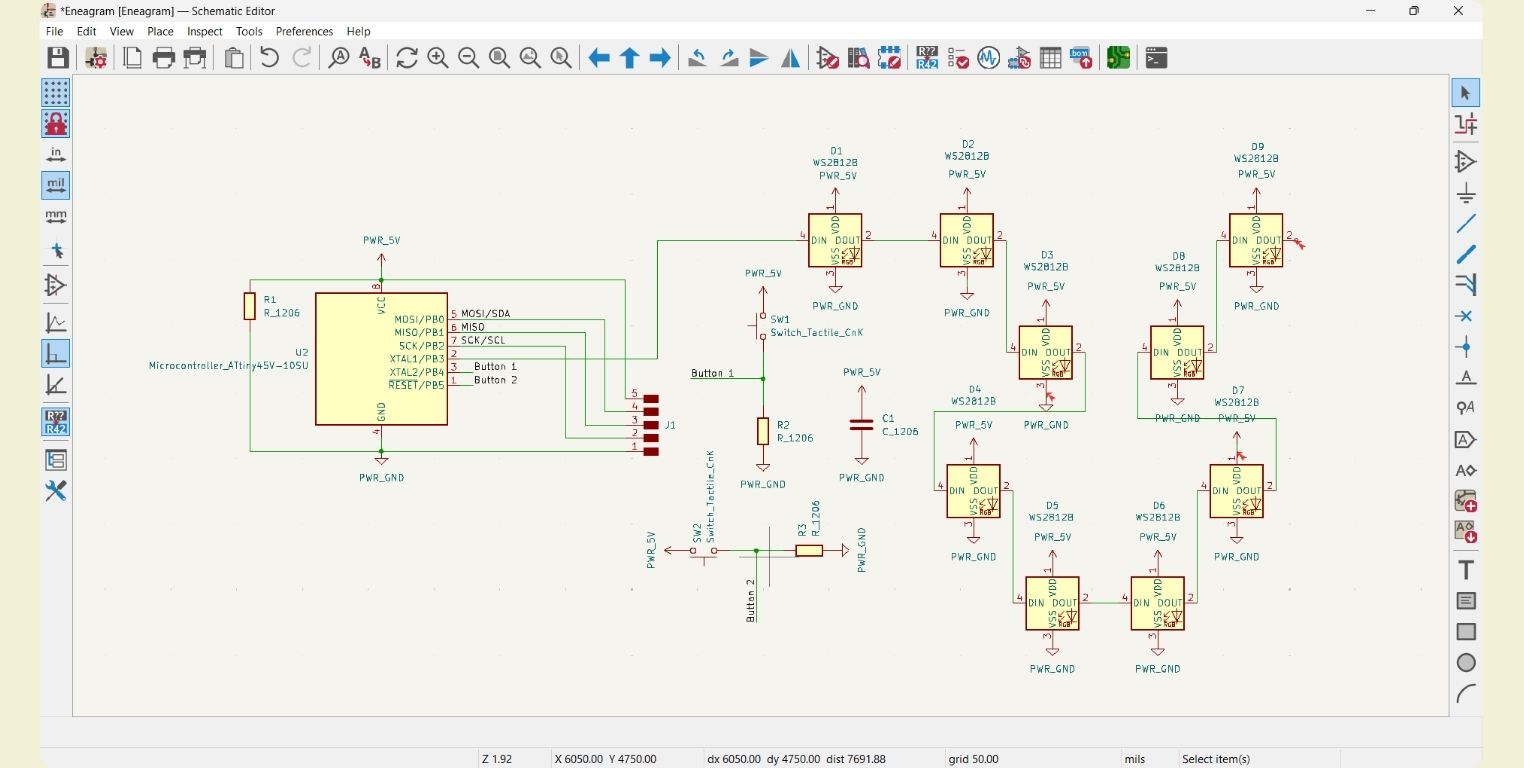
Try to find the mistakes in the following picture!
As seen in the picture below, I also connected a button with its respective resistor (I know that in the picture there are 2, but in the end, I decided to leave only one button), and a capacitor. In addition to that, you can also see a resistor connected to voltage and ground, what does it do there? I don't really remember why I put it there, I just remember that I ignored it for a while and then it gave me a headache when arranging the components, but I'll tell you more later.
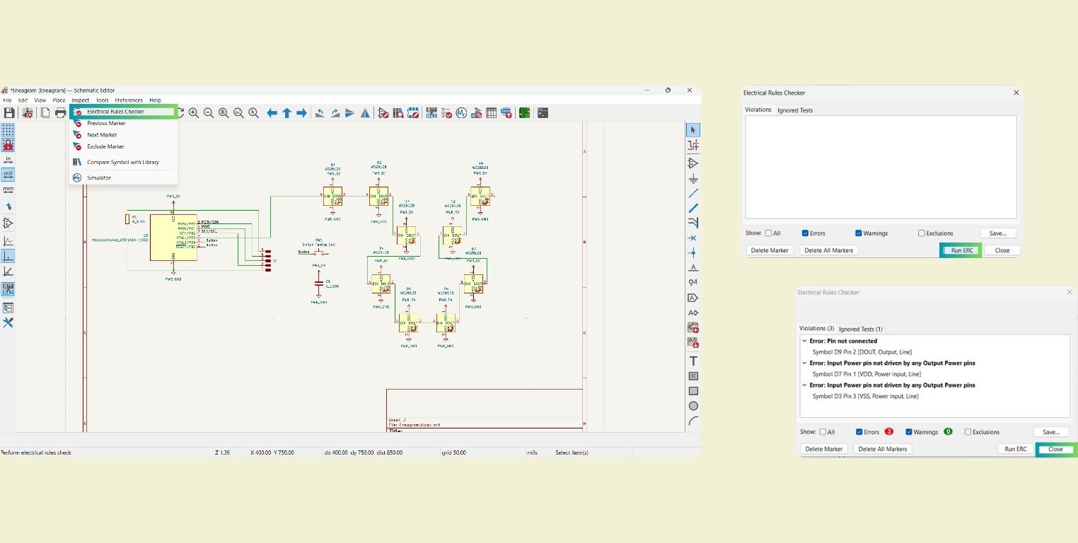
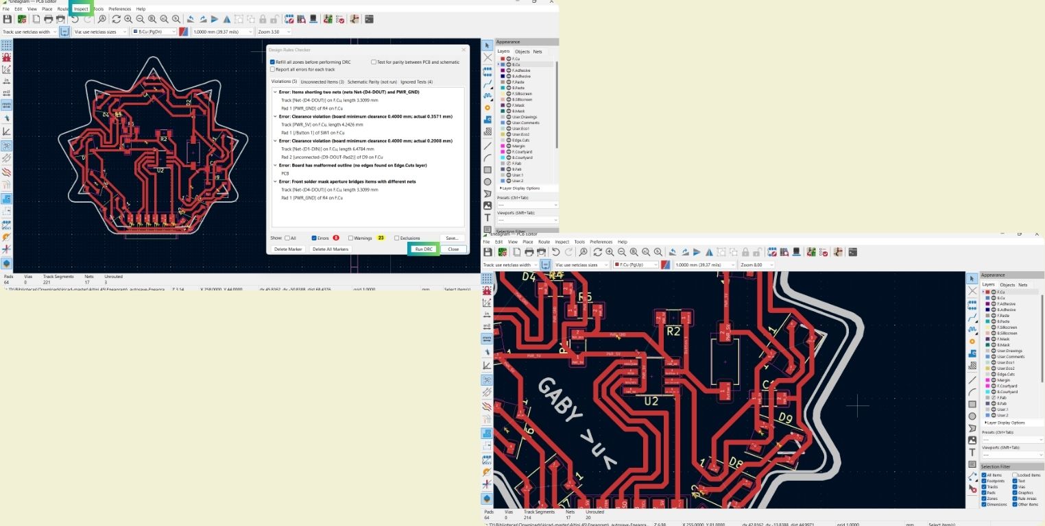
To verify that there are no errors in the schema, within the "Inspect" menu select "Electrical Rules Checker". What it does is open a tab, click on "Run ERC", and then the possible errors that it could have appear.
Design Process
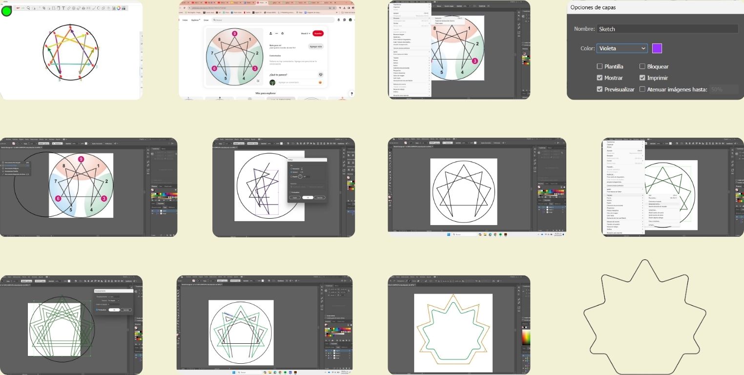
Before continuing, I decided to design my PCB, as I would need it to accommodate all my components. Initially, I wanted to continue with the idea of my project and make the top part of the lamp from my final project, however, the size I want it to be is too small to do it on a PCB, so I think in the future I will try to replicate what I did, but with a strip of Neopixels made of vinyl.
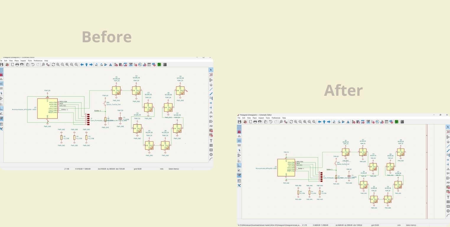
Returning to the design, I wanted my PCB to follow the shape of the enneagram with the paths, so I drew it circular, with the Neopixels around and the paths connecting. Then I passed it to Illustrator, because I naively believed my idea was possible, and maybe it is, but not in the size I thought, also I would have to add many resistors for the intersection of the paths... So what I did was make an offset of my stroke, and leave only the outline. Once ready, I rounded the corners and exported it as DXF.
PCB Editor
I went back to KiCad and in the top menu I selected the "Open PCB in board editor" icon, it opens a dark tab, there within the "Tools" menu I clicked on "Update PCB from Schematic...", it opens a tab with all the changes that can be applied, because yes, you can go back to the previous scheme and update the changes in the new one (I did it several times), finally click on "Update PCB" and we can see all the components on the screen, although they still need to be arranged. For this, I went to the "File" menu where I imported the document I had previously made in "Graphics".
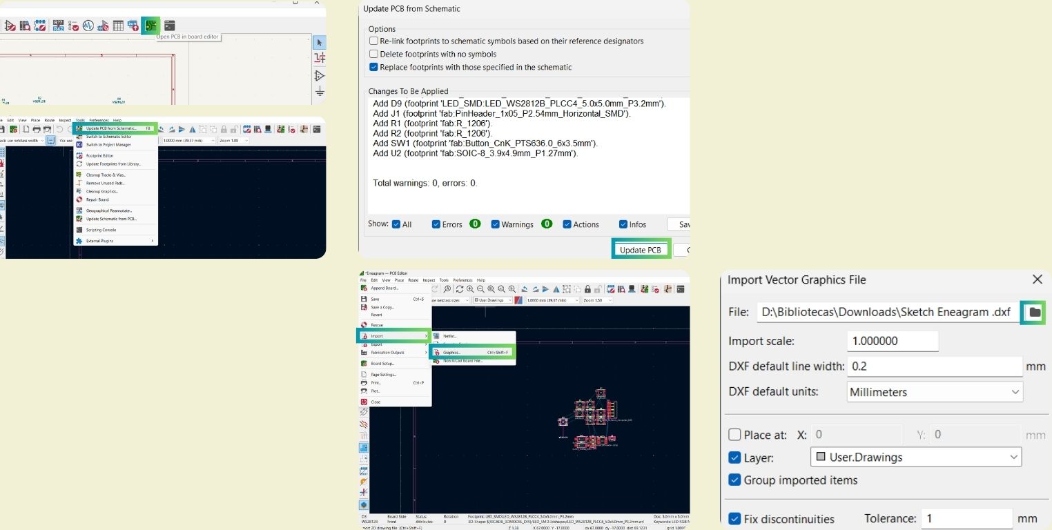
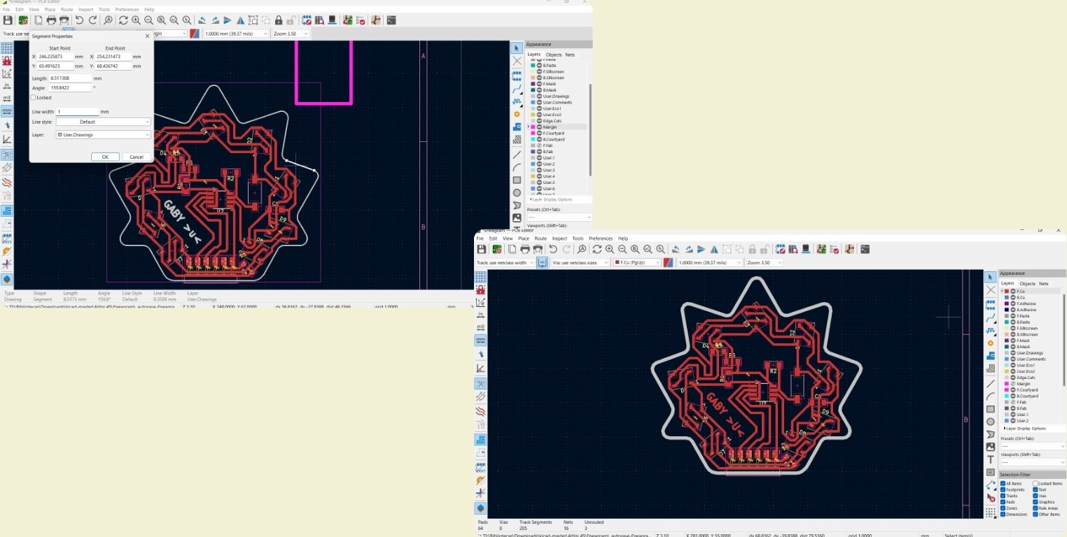
The next step is to configure the design rules. For "Clearance" I gave it 0.4 mm, and for "Track width" 0.7 mm. Once that was done, I was able to arrange the components as I wanted, and with the letter "X" I was able to start drawing the connections. To rotate the components, just double-click on the component you want and in the lower right corner adjust the degrees, or simply select the component and click on the letter "R".
Once you think you have connected everything, within the "Inspect" menu you can verify that this is the case. It showed me many because at some point "Ground" had disappeared and had become voltage, and do you remember the resistor I had connected? Well, I had removed it, but I left the connection between voltage and ground. You can also see in the photos below, that I added 3 resistors that were connected only to ground, and that is because I arranged the components so that ground was on the outside and voltage on the inside, however, the components inside must also be connected to ground, but as I no longer had space to pass a ground path to the center, what I did was make resistor bridges with a value of 0 connected to ground.
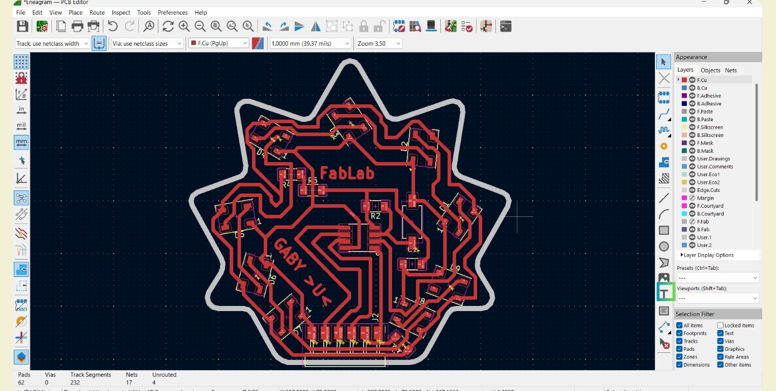
Here you can see a photo of how it turned out (until it was modified by a suggestion from an instructor and I added an LED to it). To add text, you can easily do it in the icon that has a "T".
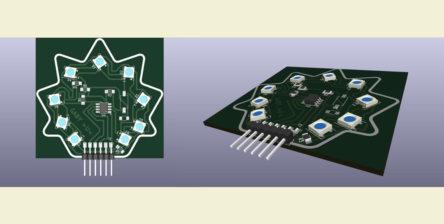
Something that fascinated me was that KiCad has the option to see your PCB in 3D.
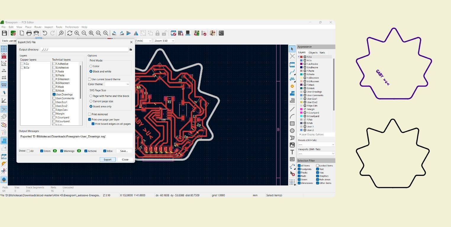
The next step was to give thickness to the contour I had made. For some reason in the program, the strokes became ungrouped, so I had to do it stroke by stroke. To do this, double-click on the stroke and change the width to 1 mm. Future Gaby's recommendation: give it a thickness of 0.1 mm larger than your cutting tool.
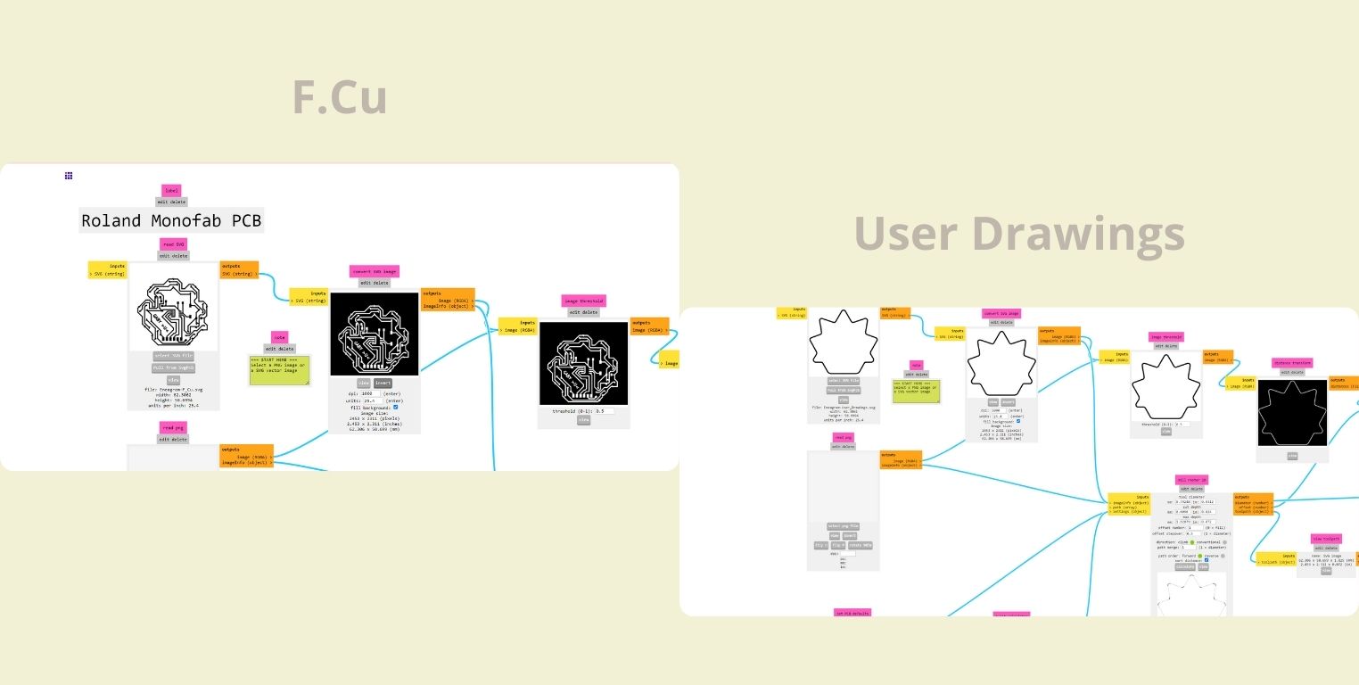
To export the engraving and cutting part, it must be done in SVG format. The first thing I exported was the cutting outline that was on the "User.Drawings" layer, but I had a problem the first time I tried it, and it is that as you can see in the blue drawing, the text I had added was in this, if I left it and manufactured the PCB like this, then the text would be cut. So what I did was change the layer of the text. And so I only got the SVG file of the outline.
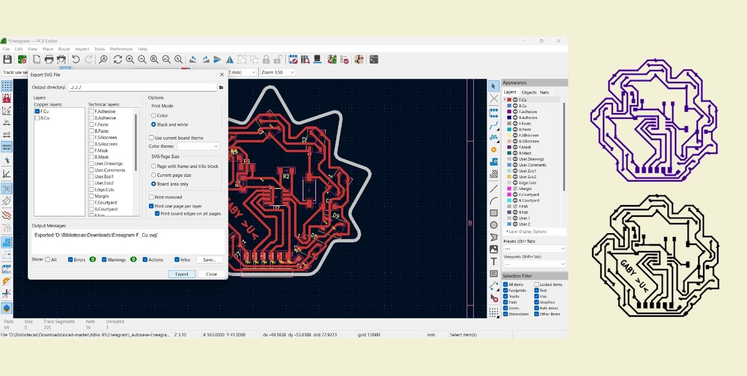
The next file I exported was the one that would be done with engraving and it was found in the "F.Cu" layer. Something important for both this and the previous one is to verify that the printing mode is in "Black and White".
Join me in making it!
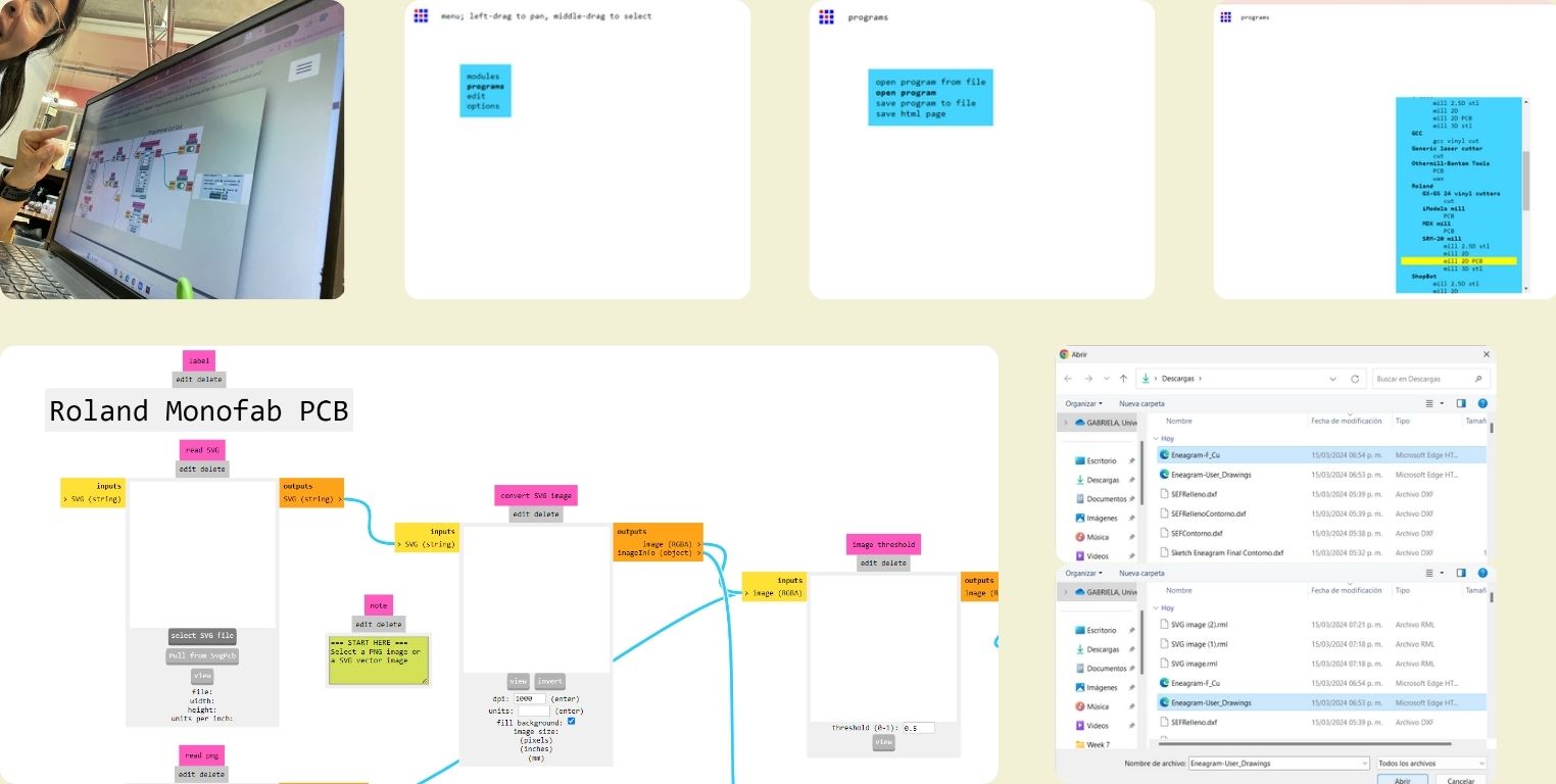
As you can see in the first photo, I was very excited because I went back to see the documentation I made in week 4. I'm really satisfied because this was useful to me in the future.
Basically, I followed the same steps as that week, so I invite you to visit it so that you can understand in more detail.
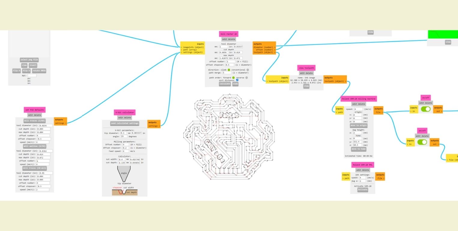
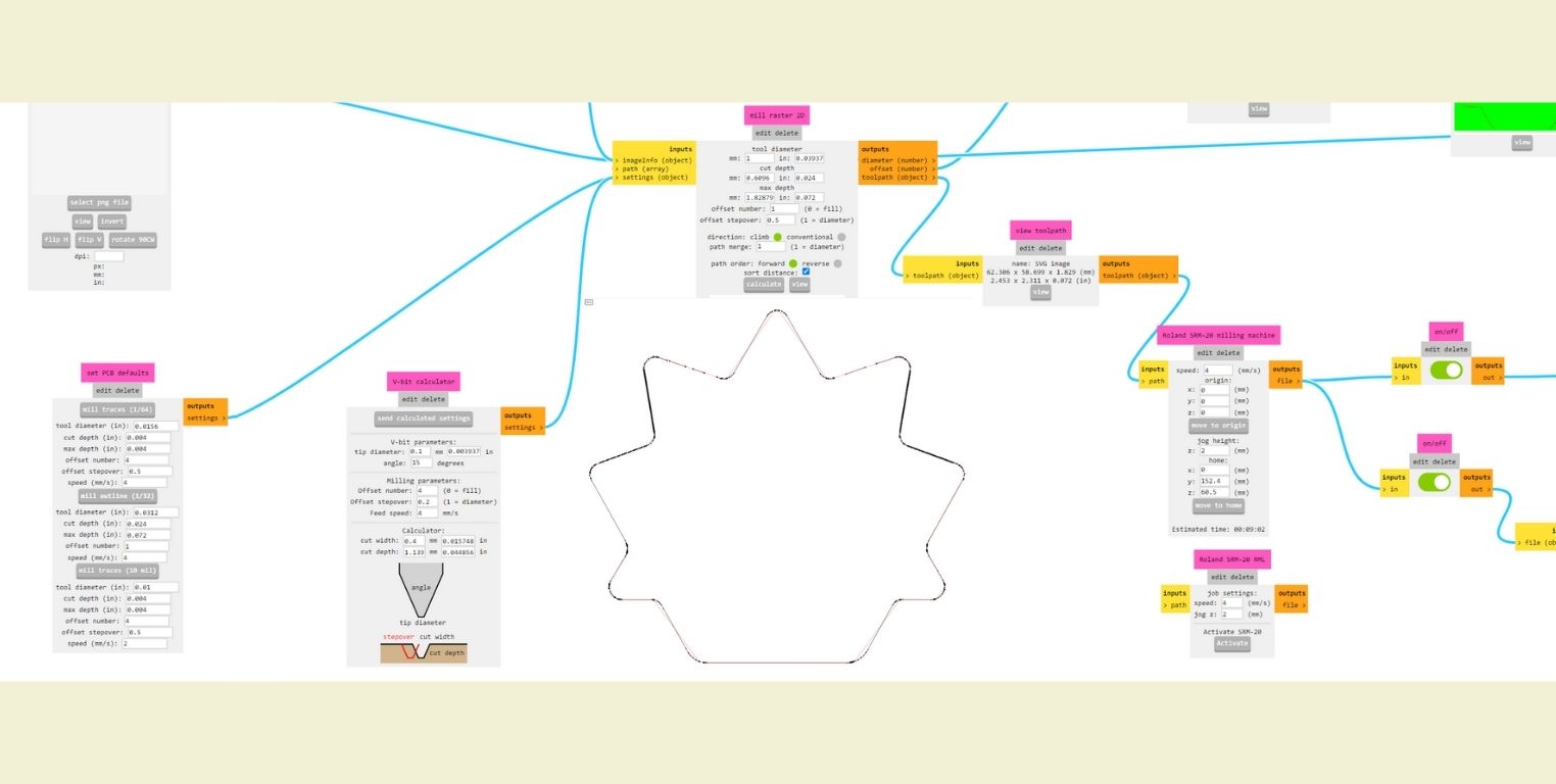
I opened Mods and chose the SRM-20 mill 2D PCB and in the Read SVG section, I selected the SVG file for engraving and cutting.
For the engraving file, I inverted the colors. For the cutting file, this was not necessary.
Here is an overview of the configuration for the files.
Once I downloaded the files, it was time to prepare everything to cut with the machine. And of course, I continued to rely on my documentation.

The first thing I did was place the engraving piece... and it fell, I thought I had lost it, but I discovered that there is a drawer under the machine, and you can recover everything you have dropped. The next thing was to manually make the holes in my sacrificial table larger because the screws were larger than the ones I had.
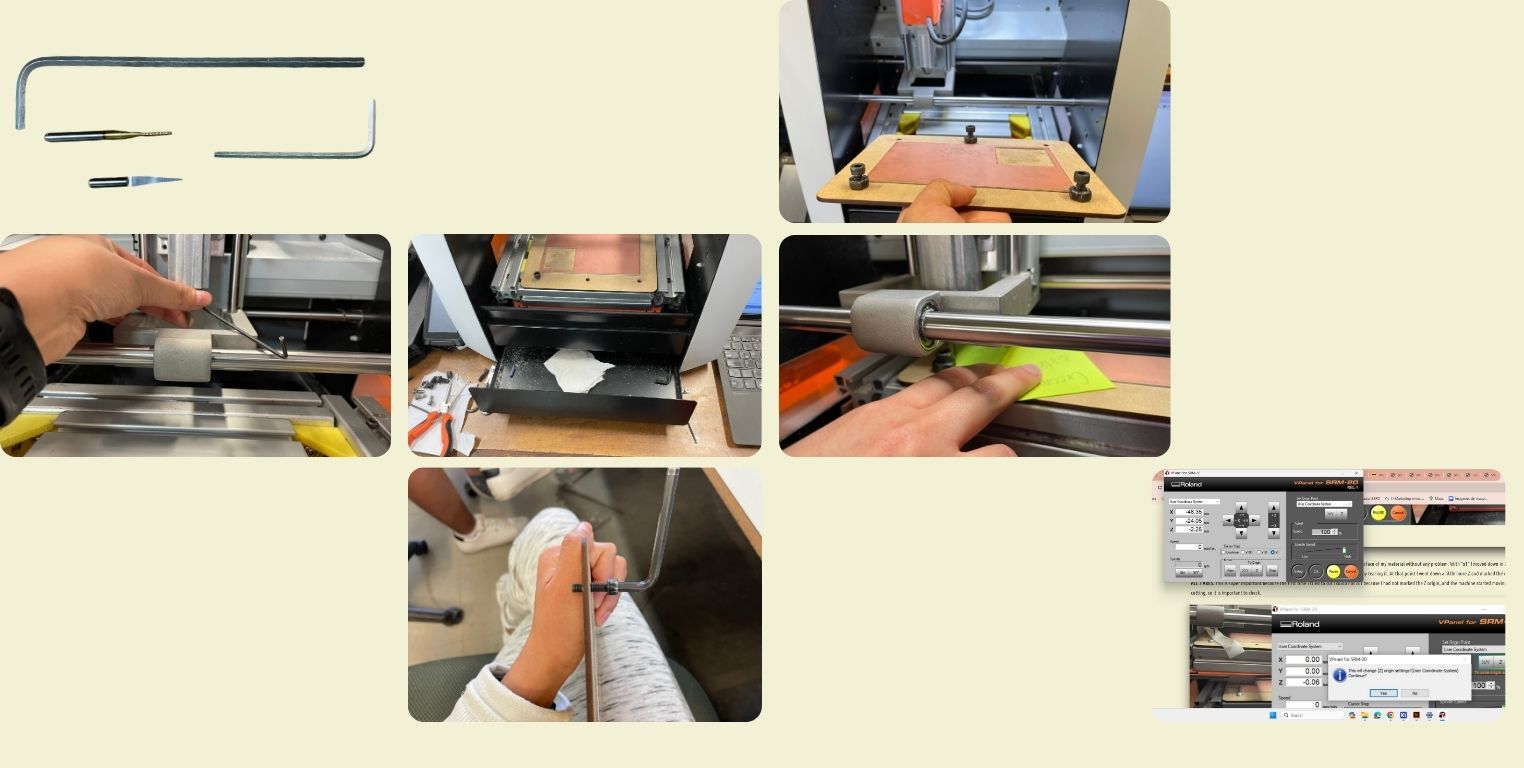
I moved the tool to the origin I wanted in X and Y, and then I used a paper to adjust the tool in Z. Once I saved the origin in the 3 axes, I uploaded the corresponding file. First the engraving and then the cutting.
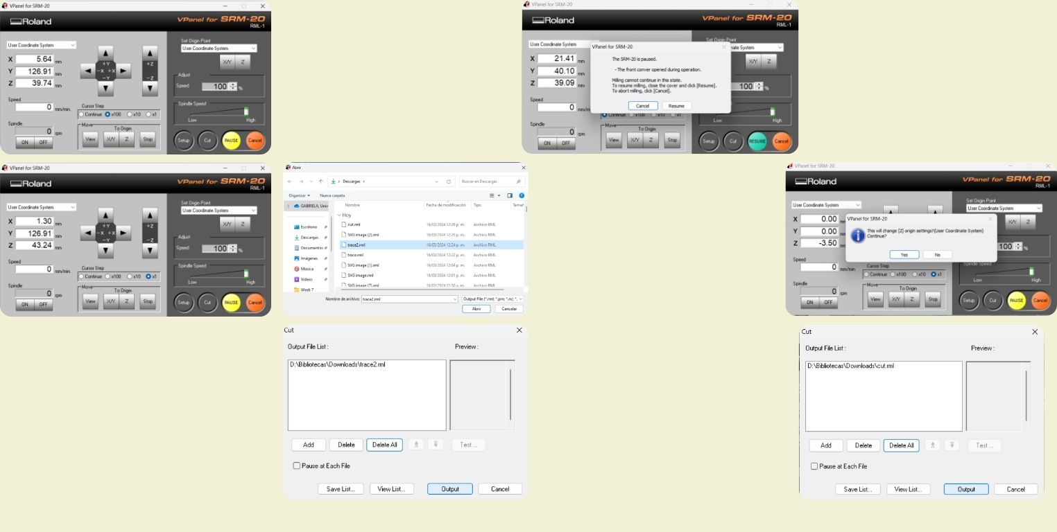
My first attempt did not go well because the machine was misaligned. You can check by moving the tool in the X and Y axes to verify that the Z position does not change when moving in these axes.
In my second attempt, it went smoothly, after someone calibrated the machine. However, some parts of the contour were not cut, and I had to cut them with a cutter by hand. What an instructor told me was that because of the shape in some sections, it could be that my line was not 1 mm, but smaller, and therefore the tool did not even attempt to cut it because it was 1 mm. That's why it's better for it to be 0.1 mm thicker than the tool.
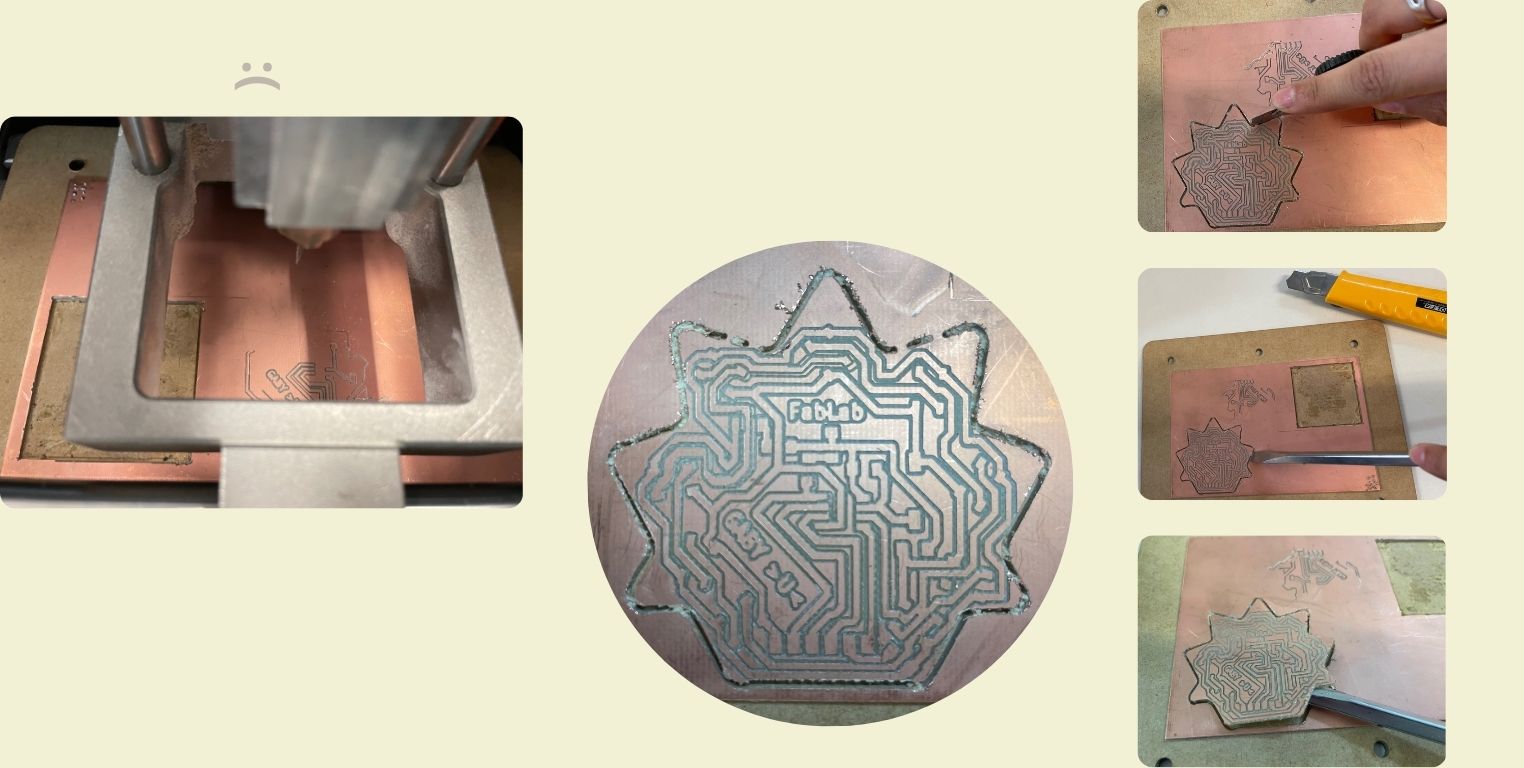
Let's Solder!
I think this is my favorite part of the whole process, for me, it's already a ritual, and although I know I don't do it perfectly, at least I enjoy it. I prepare my workspace, put background music, and the view of KiCad to know the position of the components, and I also do a physical preview.
I always start with the smallest components from the center towards the larger ones at the ends. But at one point I realized that the resistor that is connected to the LED I added at the end did not connect to ground, so I had to improvise with a 0 resistor to make a bridge and connect it to ground.
For the Neopixels, I took special care because like the microcontroller, the pins it has go in a specific place, so I used the picture below to understand how they were soldered.
After finishing soldering, I checked that the components were soldered well and that there were no wrong connections with tin using a Multimeter. This small device helps measure continuity, current, resistance, and voltage. You can learn more by entering the group assignment for this week.
TIME TO PROGRAM!
For programming, one of our instructors provided us with a guide to program the ATTiny 45/84/85 and ATtemega 328.
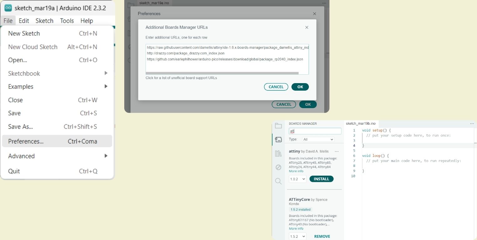
In Arduino, within the "File" menu, I clicked on "Preferences" to manage the ATTiny URL: https://raw.githubusercontent.com/damellis/attiny/ide-1.6.x-boards-manager/package_damellis_attiny_index.json
After that, I installed the "ATTinyCore by Spence" library.
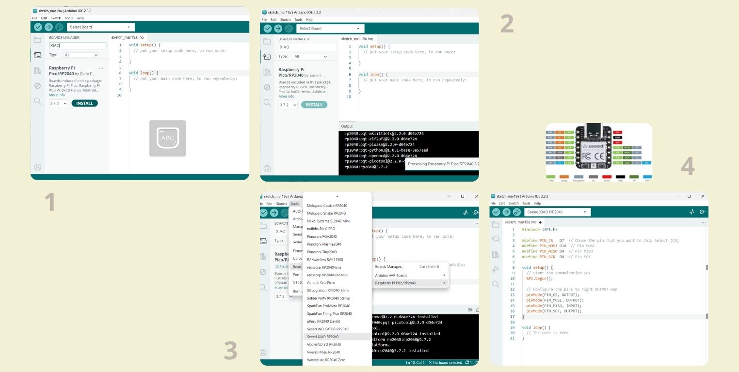
Initially, I tried to do the programming using the first PCB we made in week 4, with the XIAO RP 2040, here you can see the code I did to define the pins that would be connected to the XIAO, however, it did not work as expected and a classmate of the course recommended me not to complicate things and do it with an Arduino Uno.
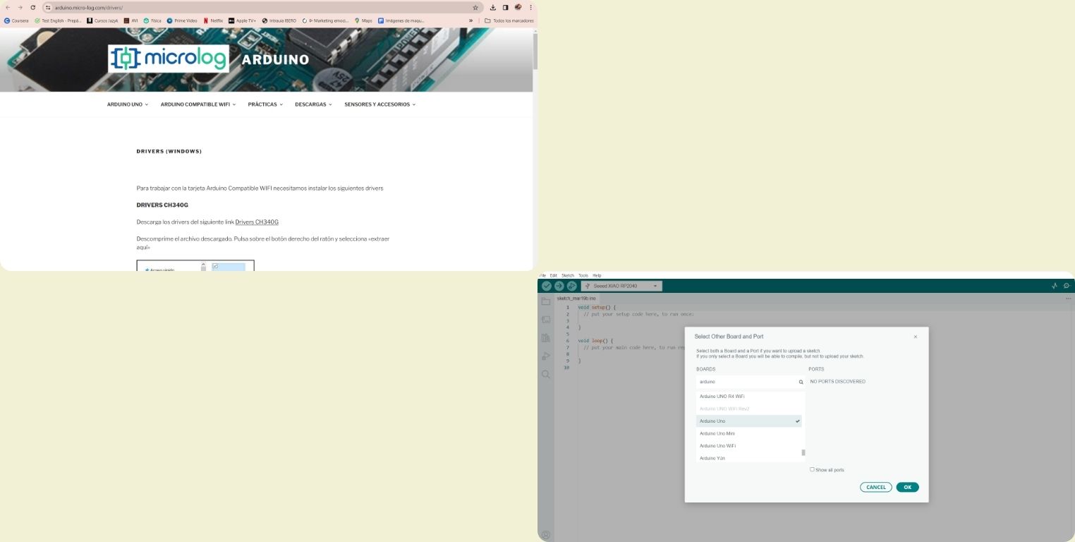
Even so, the Arduino Uno had its complications because when connecting it, I couldn't recognize it, not even after installing the library. An instructor told me that maybe I didn't have a driver... After a while, I found this page that explains how to install it.
The next step was to search within the "File" menu for example number 11 "ArduinoISP". Then in the "Tools" menu, I selected "AVR ISP" as the programmer and loaded the example code to the Arduino Uno.
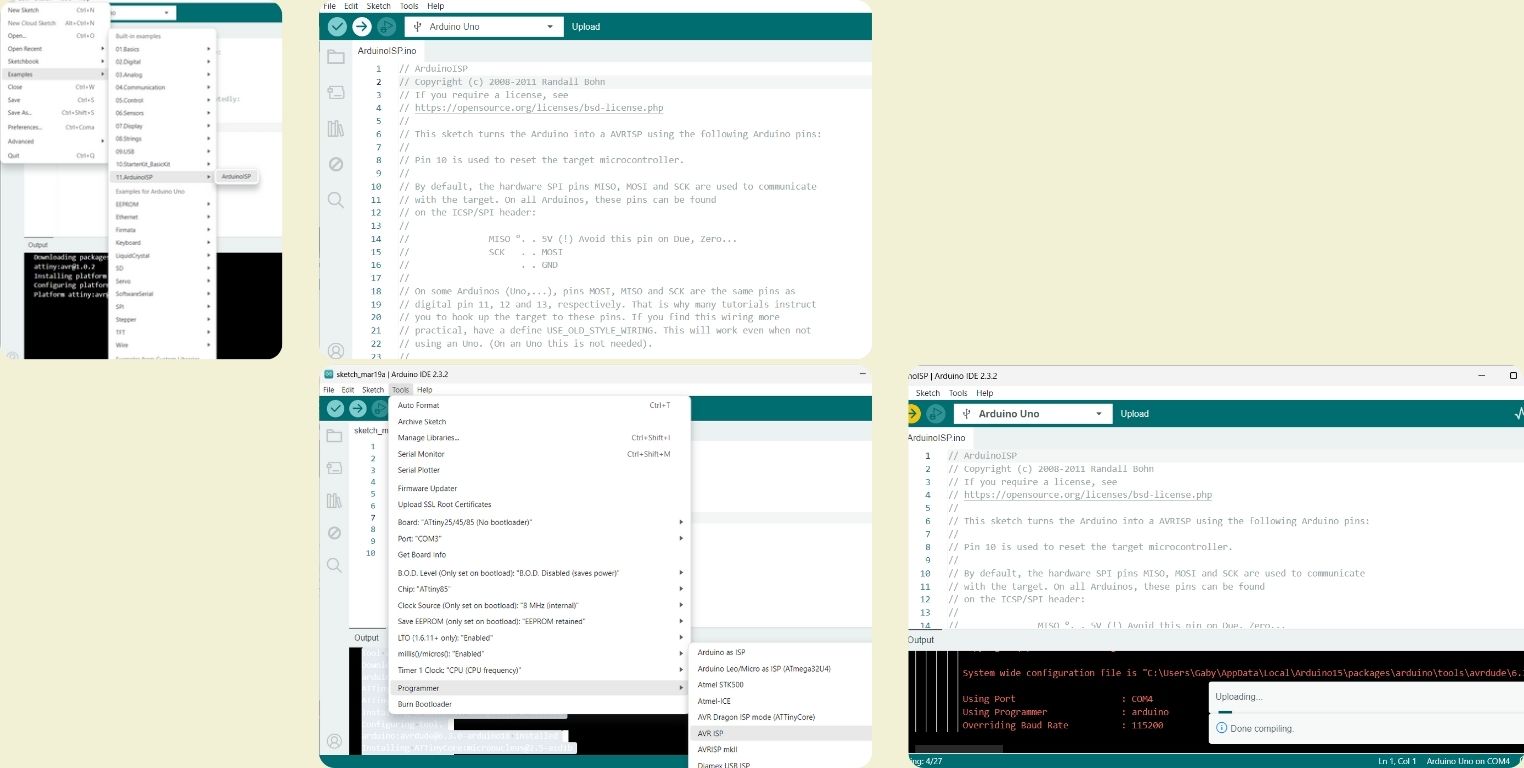
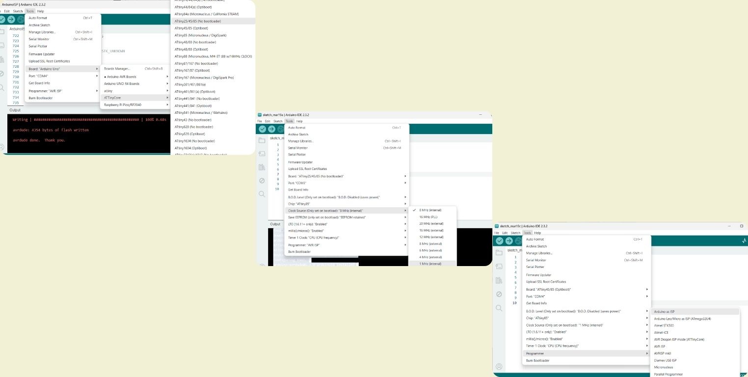
It is time to change the Arduino Uno board to "ATtiny25/45/85 (No bootloader)", select "1 MHz (internal)" for the "Clock Source" (for Neopixel, "8 MHz (internal)" should be selected), and finally choose "Arduino as ISP" as the programmer, all within the "Tools" menu.
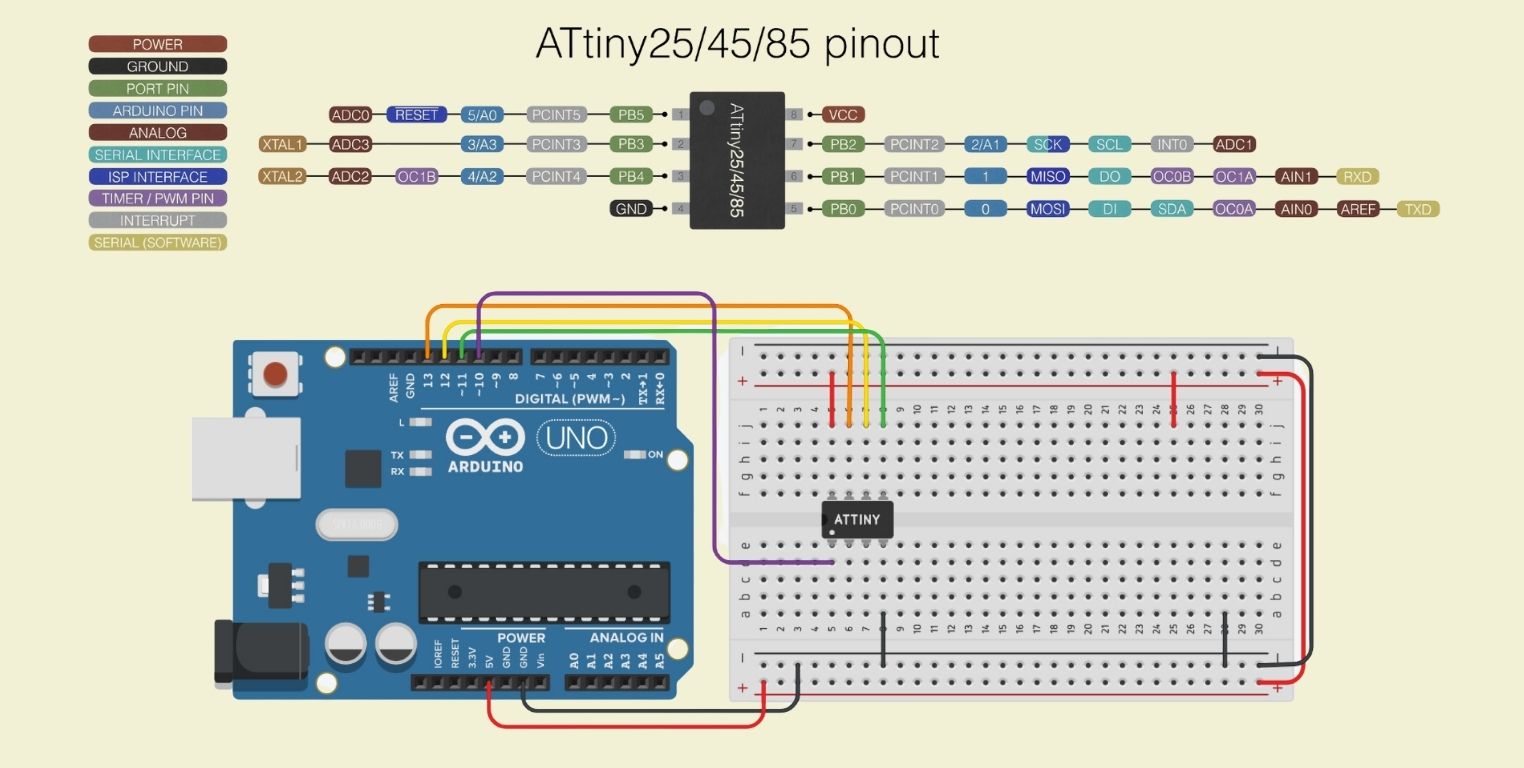
To connect the Arduino Uno to the board I made, I used the following diagrams:
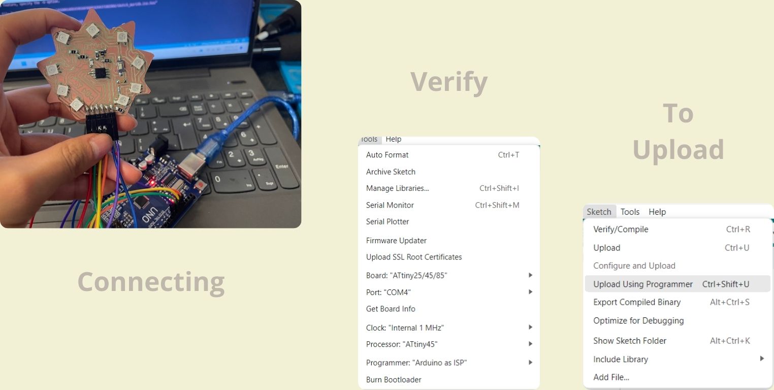
Before starting to program, it is important to check within the "Tools" menu that everything looks like in the photo below. It is also important to note that to load the codes it is necessary to do it from the "Sketch" menu by clicking on "Upload Using Programmer".
In my first attempt to turn on the LED, it didn't work as expected because I wasn't writing the PIN to which it was connected correctly.
When I changed it from 5 to PB0, it worked correctly!, that means I didn't burn the microcontroller when I soldered it.
Then, I tried to program the Neopixels, first using the example called "simple" found in the "File" menu within the "Adafruit NeoPixel" library. From the example, I only changed the PIN to which the first Neopixel, which is connected to all the others, is connected, and the number of Neopixels I am using on this board.
At first, it didn't work for me, until I changed the clock to "8 MHz internal".
When it worked, only one Neopixel lit up (the last of the 9), that made me realize that the track connecting the microcontroller to the Neopixel line was also making contact on the last of this row, so all contact with the others was lost. To fix this, I had to remove the neopixel and separate the tracks with a cutter. Then I tried to turn on only the first Neopixel to verify that it had worked... so that you don't go through what happened to me in the video, keep in mind that in a line of Neopixels, the first one is called 0, and the second one is called 1, and so on, I had done it first with 1, that's why the second one lit up.
To understand this, I had to try another code before effectively loading the example code. And as if nothing happened, it worked, because I had the principle I explained before. It was as if it was mocking me because the day before I wasn't sure what wasn't working, and in the end, it was just a mistake of a number in the code.
This is how the example code looks when it is working successfully.
Then I tried to turn on all the Neopixels at the same time.
In the following code, I turned on each Neopixel, one at a time in the order of the clock hands, and at the end all the Neopixels at the same time.
Having practiced with the Neopixels, I tried loading a code where the Neopixels light up according to the order of the Enneagram when they "go to their center". The Enneagram explains that each personality type can center and go to its most authentic state when it moves to the positive of another to which it is connected, this is how the representative diagram of this is created.
Finally, I added the button, to activate the last Neopixel code I made.
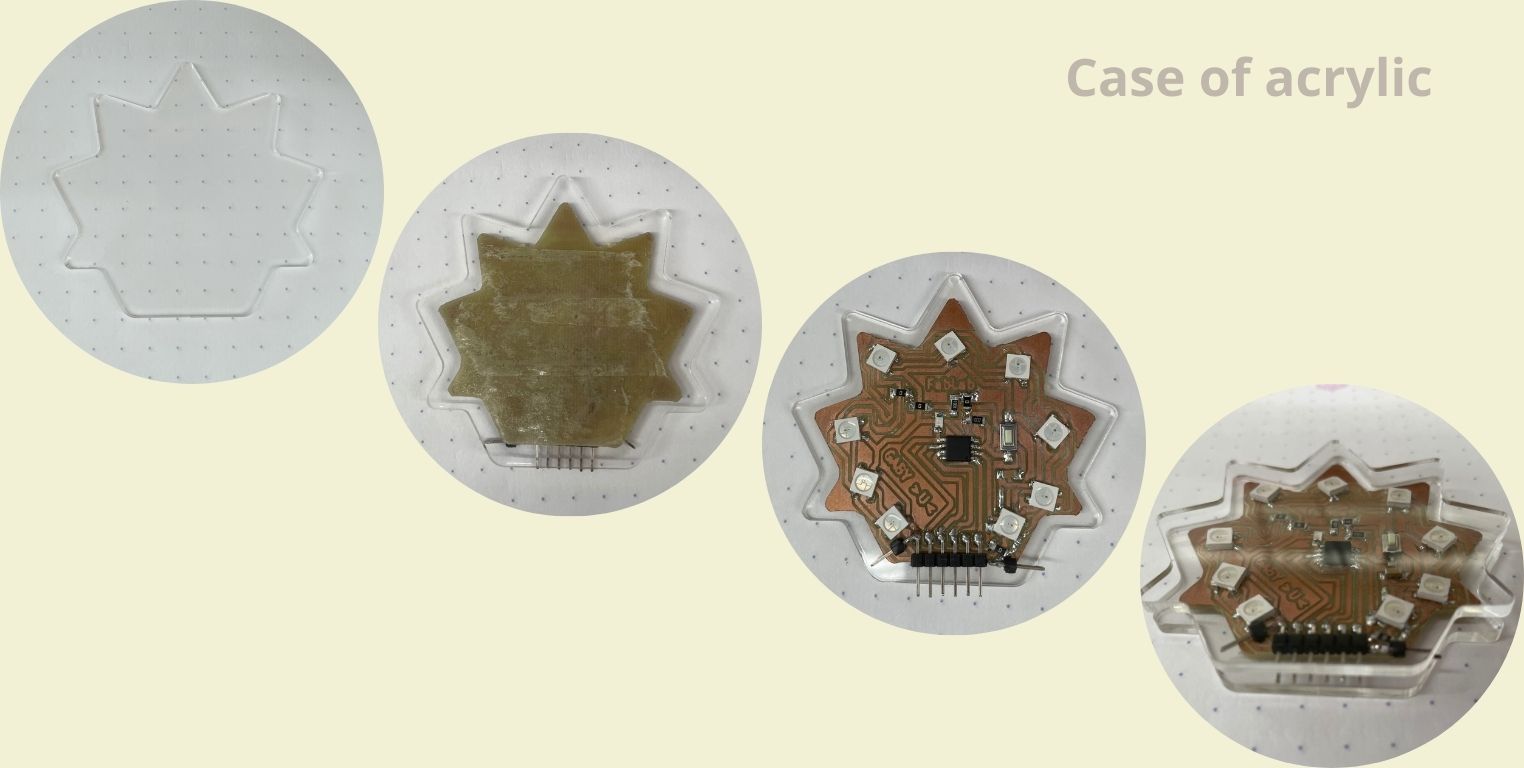
Case
I wanted to do a case for my PCB, but I didn't know how to do it while still having access to the pins, so I decided to do a base of acrylic. For that I hat a idea of bending acrylic with heat, but in the end I chose to stick my PCB with tape to the acrylic base, and ovelapp another similar base on top. I think it looks pretty.
Also you can see that I have added two more pins at the ends of the pcb to connect ground and voltage in case I need it. At the moment this is the most delicate thing I have to protect so they don't come unstuck.
Conclusion
I think this has been the longest practice I have done so far, I loved and hated it at the same time. I can't believe I'm finishing documenting it because it became so extensive, I was working on it the whole week, and it was a total challenge. In the end, I must say that I am quite happy with the result I got, and I also see a little of what I imagine for my final project.