

My Final Project: The Campus ROVER
P4 - Digital & Power Electronics
The electronics needed for this proyect are divided in two boards: The controlboard, dedicated to the microcontroller and its accompanying hardware, and the powerboard, containing all the power electronics needed to control the motors and regulate battery voltage. Both boards were sent to a PCB manufacturing service for fabrication, as they deliver much better finishes and quality than those that are possible using local equipment, allowing for tighter tolerances, thinner traces, double-sided boards, reduced size, and overall better functionality and aestethic appeal. So, the designs shown here are not thought to be easily made using standard equipment! Nevertheless, nowadays PCB fabbing services are easily accesible and often have fast deliveries!
The Control Board:
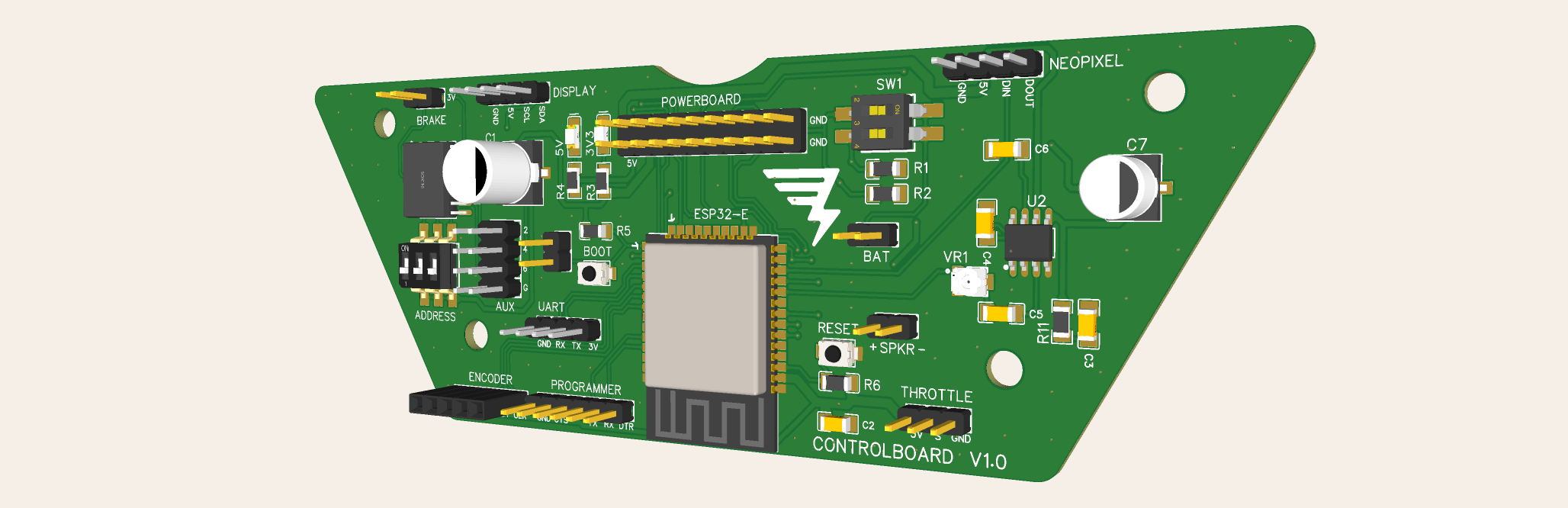
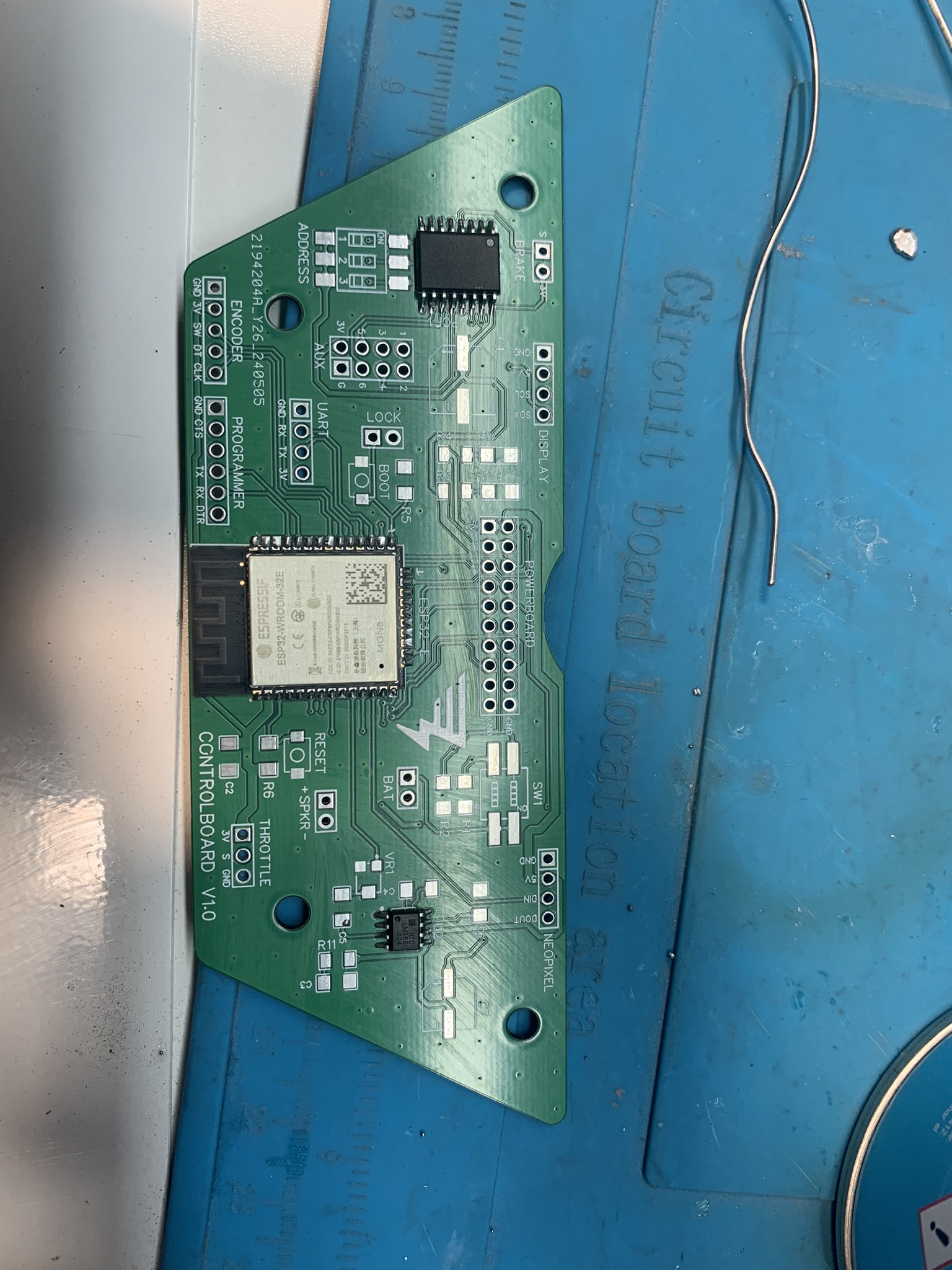
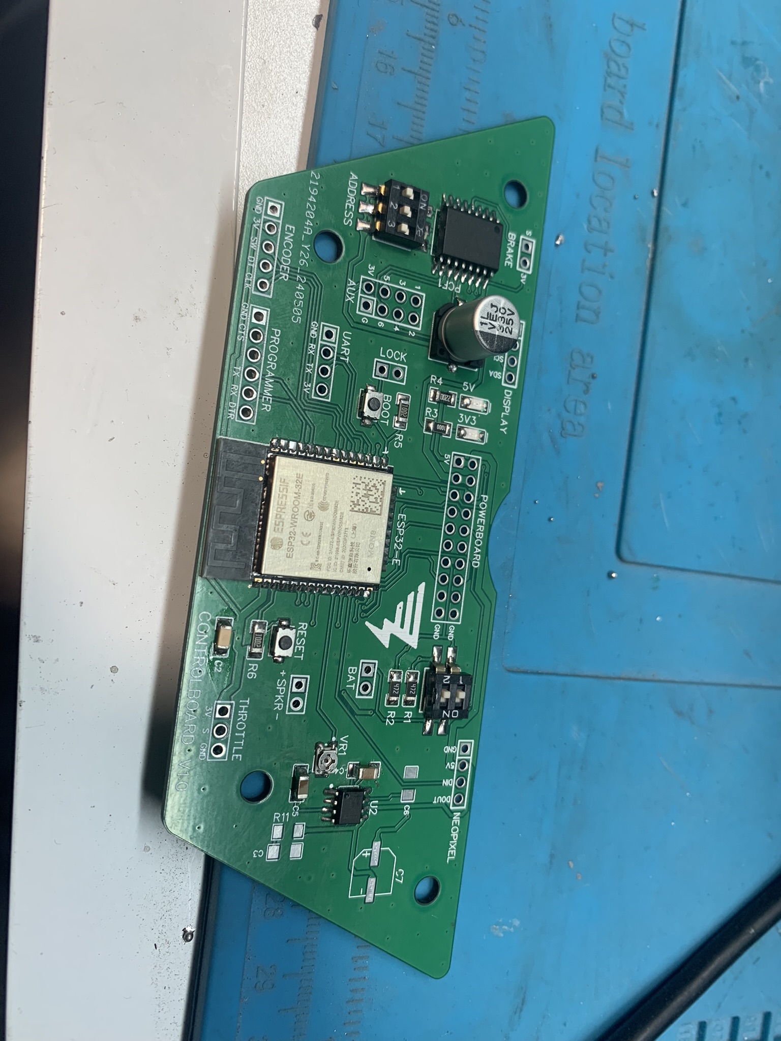
The control board is the least complex board of the two, and contains the following characteristics:
- An ESP32 microcontroller to handle all the scooter's control and communication needs.
- Accompanying hardware for the MCU such as Boot and Reset buttons, a capacitor for power fluctuations and a programming port.
- An audio amplifier connected to the ESP32's internal DAC, used to create more complex sounds.
- An I/O expander for controlling anything I may not have planned for ahead.
- A whole bunch of pin headers to connect the board to the scooter's control levers and auxiliary systems.
- A 20-pin male header to connect a flat cable between the powerboard and this board.
- Power LED's to show both 5V and 3.3V voltage rails are connected.

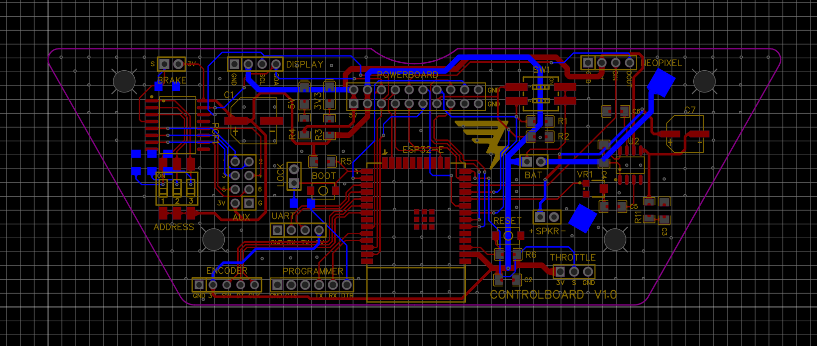
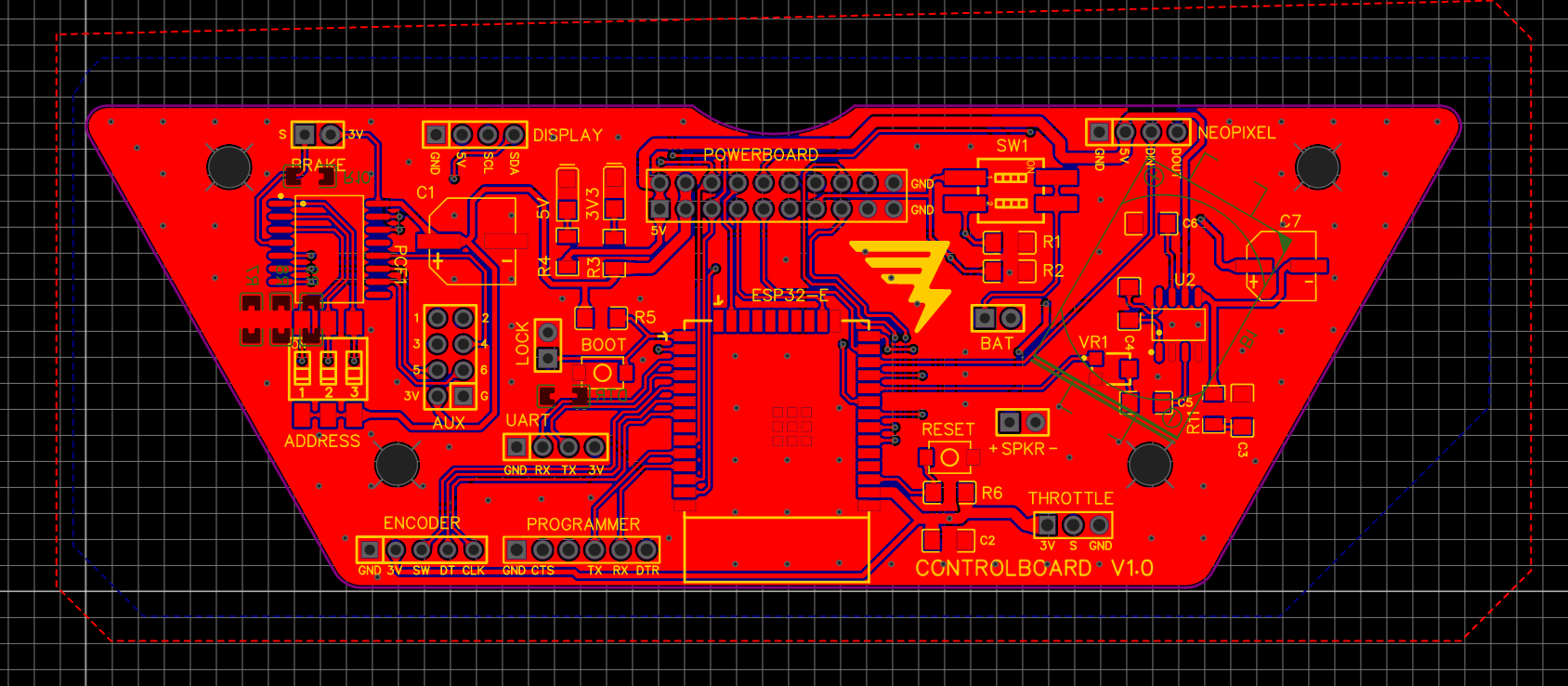
Controlboard Design:
The board was designed using EasyEDA along the following process:
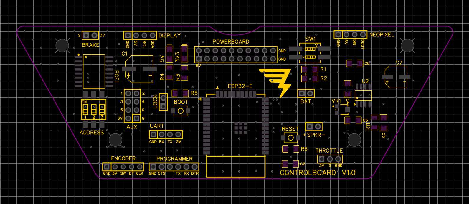
I always start by defining my board's dimensions, which in this case came from a DXF file I exported from Onshape, this allows me to perfectly match the board's shape and dimensions to its enclosure. Once the board outline and mounting points are defined, laying out the components on the board, before even I start with any routing is crucial. The main components should remain the closest to the rest to the components to ease the connections, in this case, the main component is the ESP32 microcontroller, which stands on the center of the board and is flipped 180 degrees in order to make that the comms antenna on the ESP is facing out of the board, so obstructions are minimized. Other components then surround the microcontroller and connect to it easily. Ports and connectors are left on the sides of the board whenever possible, in order to make them easily accesible.
I like EasyEDA because it offers an online component library that very rarely doesn't have the specific component I am looking for, and even if you don't find the component as is, you can try to search for the packaging and its corresponding footprint, so using this library finding everything was really easy. When placing components I like to label everything using the silkmask layer to never lose track of what I am doing.
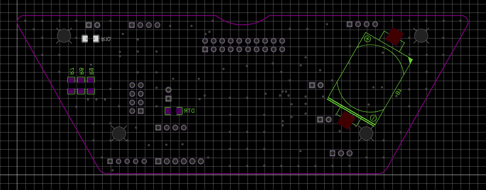
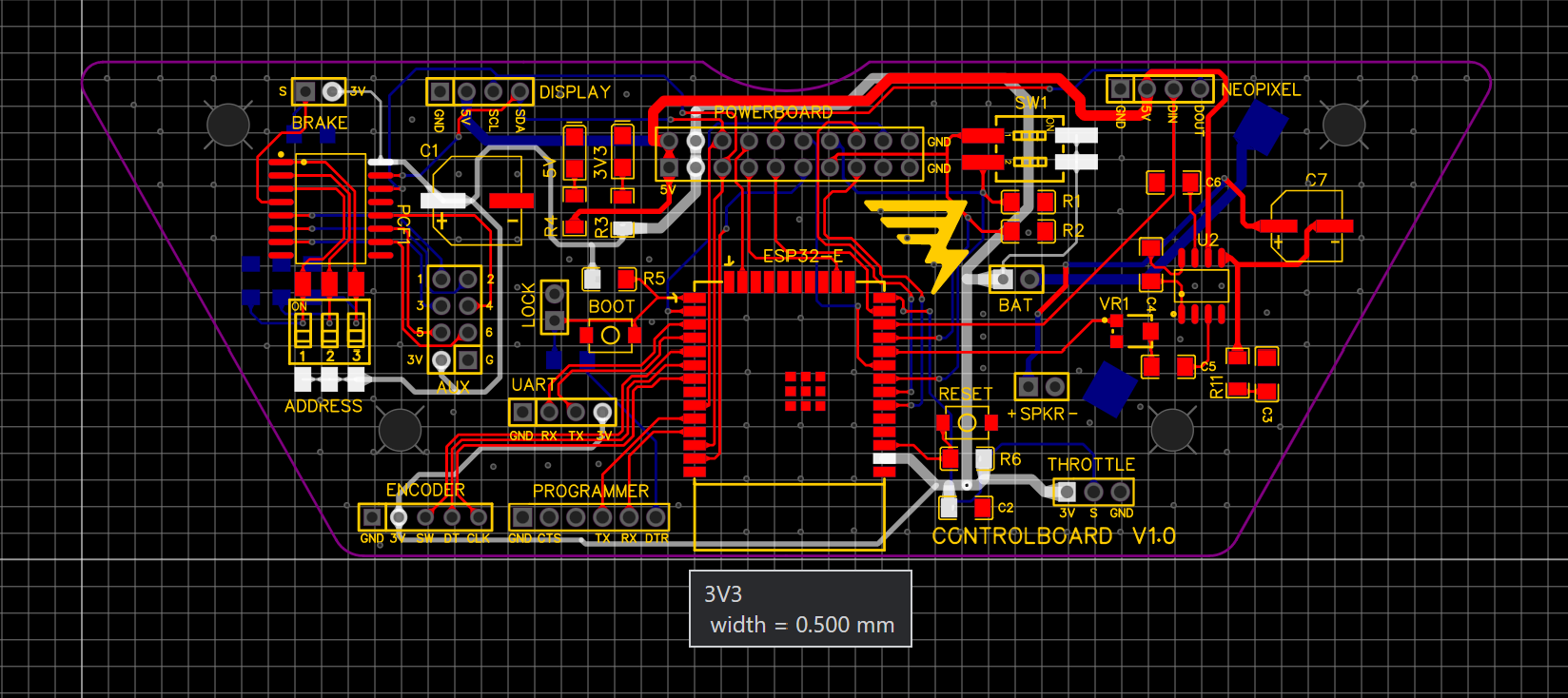
If space is limited on the board and you're using SMD components, you may consider using the other side of the board to place them, just like I did here with some small components:
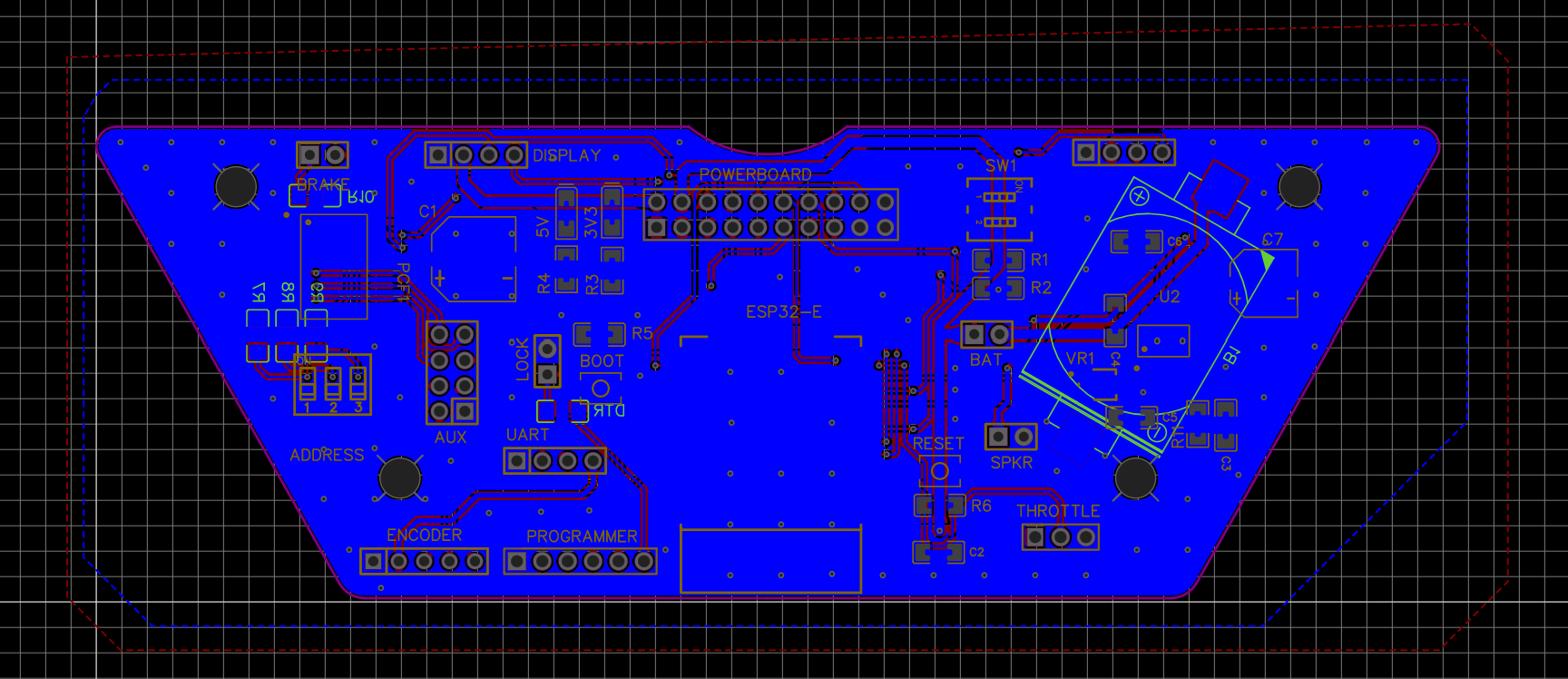
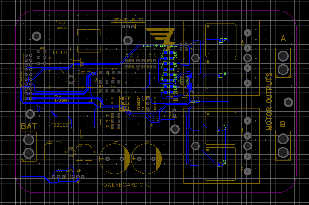
Then come the traces! In this board there's no special thickness considerations to them, so I will not explain trace calculation until the Powerboard design process, and though the traces of this board were not meticously calculated, traces that carry power to the components should be made thicker. In the images then, you can see which traces carry signals and which carry power. In the images you can also see the traces for the top of the board (red) and the ones on the bottom (blue). Having boards with two sides (or with more layers) allows for easier and more efficient connections, reducing (often to zero), the need for bridging and other techniques to cross-wire PCB's.
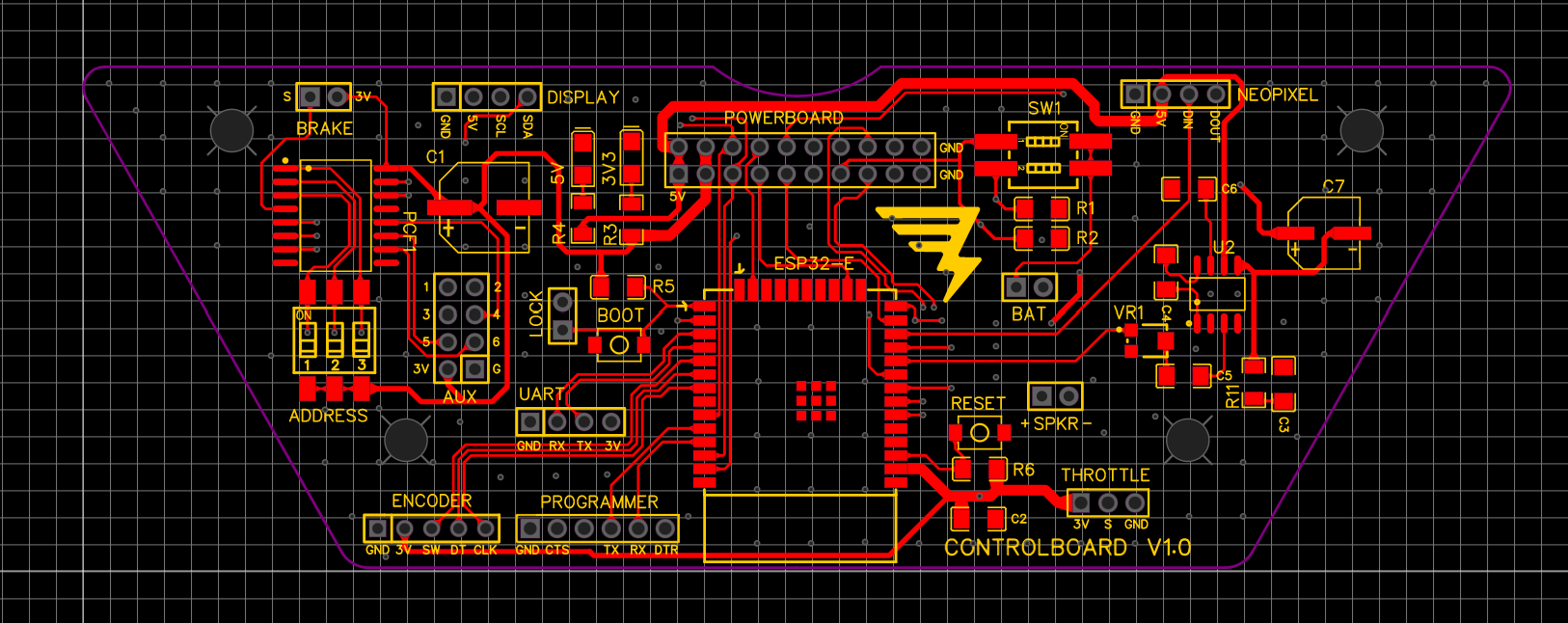
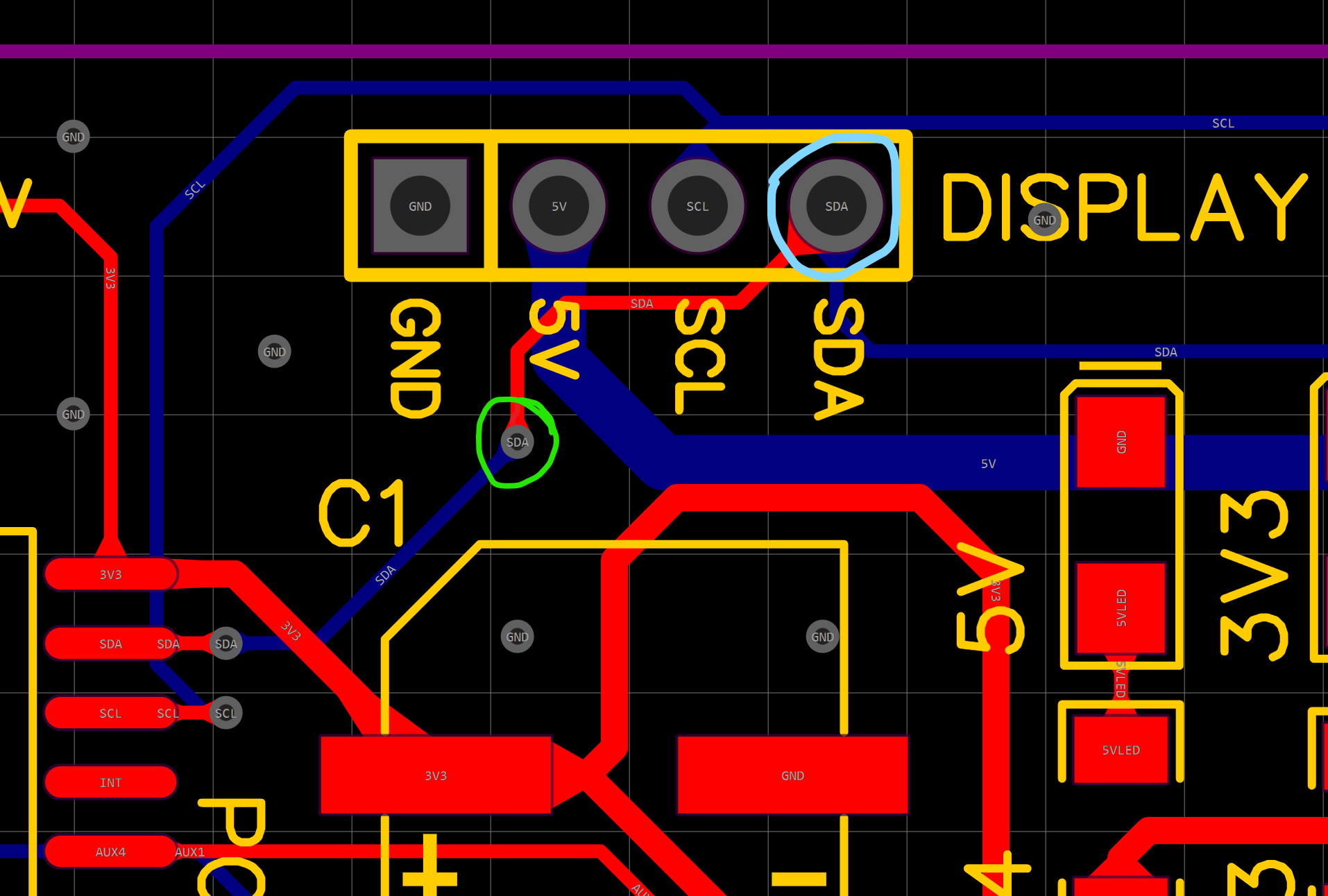
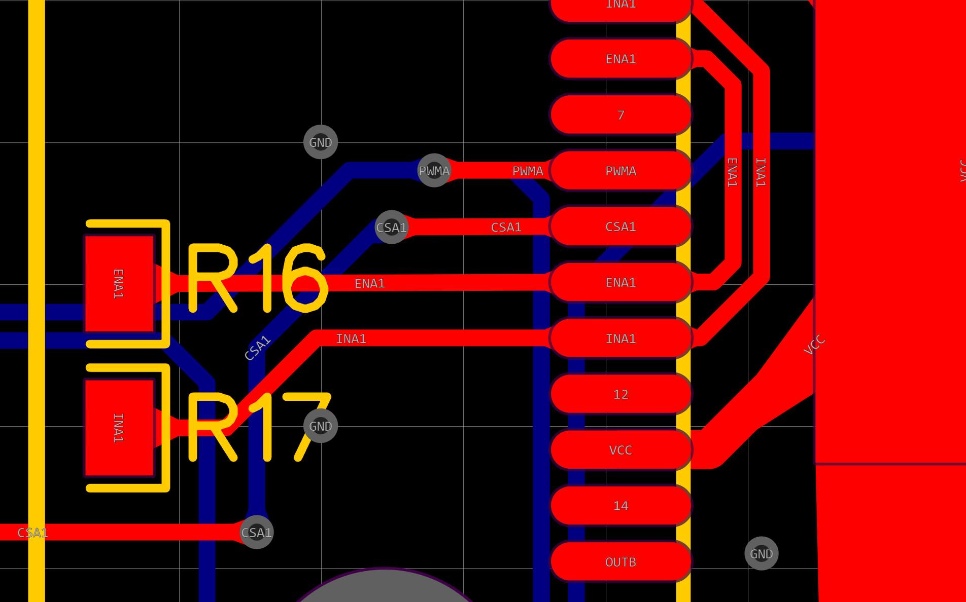
When tracing a PCB, netting is a very powerful concept in PCB design, in fact, It may be our best ally to keep connections in check and avoid all kinds of problems, from shortcircuits to forgotten connections. Netting is like assigning a function or name to a specific trace or set of traces, they mean nothing for the PCB design software besides a very important thing: This is a way for the program to recognize this traces and component pads should be connected, somehow, to each other. In EasyEDA a selected Net (Group of pads and traces with the same "name"), lights up in white to indicate they're related. The program also uses imaginary lines called "ratlines" to indicate to the user that two related traces or pads (that have the same net) are not connected to each other and you should do so, helping to never forget a connection.
In this case, the "3V3" net is highlighted when selected, this corresponds to the 3.3V power rail for the microcontroller on the board.
There are two ways to connect top traces with bottom traces: Vias and Through-Hole Pads. Vias are dedicated, often small plated holes which connect one trace on the top side to another on the bottom, as they go through the whole board (in two-layer boards) or between layers only (in 4+ layered boards). Through-Hole pads are simply holes made to connect and solder through-hole components, and we can use those holes as connections between layers if needed, but the thing is that even in 4+ layered boards, these holes always go from one side to the other. These two ways of connecting both sides pf the board are shown in the following image, where the via is circled green and the TH pad is circled light blue.
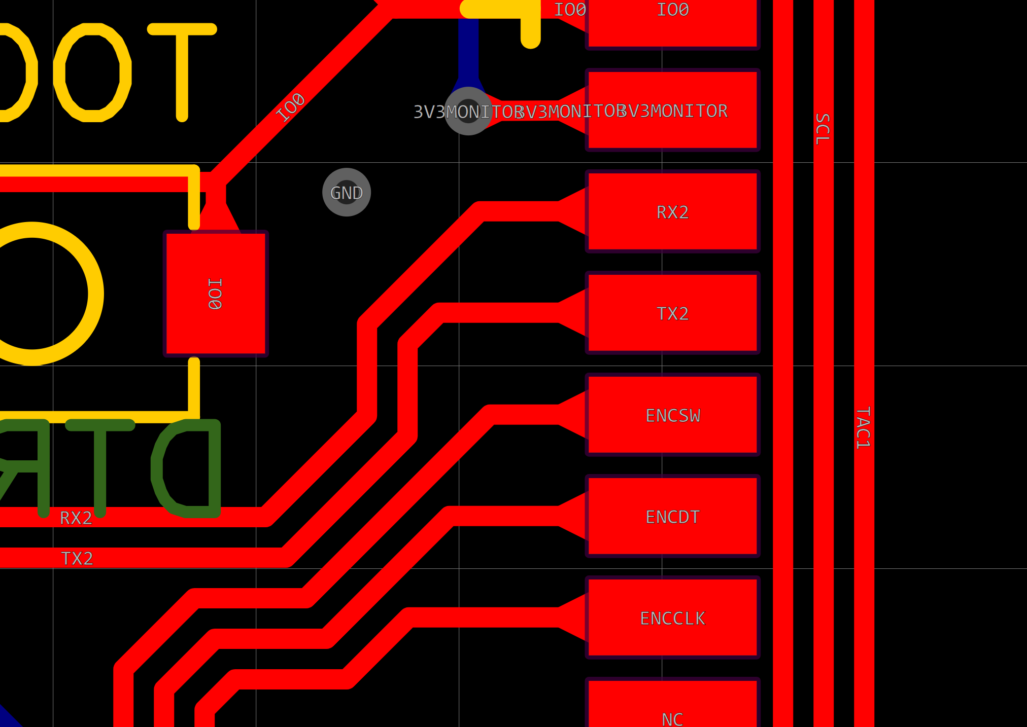
Another technique I always use when designing PCB's are teardrops, which consist of small proportional widenings of the traces when connecting to a pad. This extra copper placed on the connections makes them a bit stronger to ripping them out of the board when soldering / desoldering.
Last but not least, a ground plane is a very useful design technique that allows to convert all the unused copper (that would otherwise be removed to form the traces) into a board-wide ground connection. This has several benefits, some of which include:
- Easier routing by removing dedicated ground traces.
- Reduced noise and EMI interference within the circuit.
- Better thermal behaviour as more thermal mass is left behind.
- Faster manufacturing, as there's less copper to remove (when for example, using acid or milling fabbing methods).
- (subjective) I think it looks nicer than with all copper removed.
Even though it has several advantages, when using ground planes we should look out for this problems:
- Not advisable for PCB's or areas within them that handle high voltage (>100V DC/AC).
- Parasitic capacitance and signal loss at high frequencies (above 10.0 Megahertz)
- Relying on it for ground connections can leave components not connected if one's not careful.
- Ground connections get harder to solder due to faster heat dissipation.
If used carefully and looking out for loose connections (ratlines get real useful here), ground planes deliver great and robust results, and as my board doesn't handle high voltage nor high frequencies directly, a ground plane is a good addition. It is added to both sides of the board, as shown here:
Sending design to manufacturing service:
When designing a PCB to send into a manufacturing service we have to make sure our design is in line with the manufacturing limitations of the factory. The DRC parameters serve this purpose: They let us know how small (or big) can the manufacturing procceses used in the factory etch our design on the board, and they are usually available in the manufacturer's website. In my case I will be using JLCPCB's manufacturing service, whose DRC comes integrated in EasyEDA by default, as the software is developed by them, making all this a whole lot easier.
Before export of our finished design we click on the "Check DRC" button, which will analyze if any of our traces, vias, pads or dimensions infringe the manufacturer's capabilities. Once this is solved, we export the whole design as a Gerber file.
This file can now be imported into the webpage of any PCB manufacturer and they should be able to make it exactly the way you intended.
Soldering the Controlboard:
The PCB arrives of course empty, but with everything laid out, including the white silkmask layer that indicates easily what goes where.
SMD soldering can be a little tricky, but with some practice and the right tools the fear of braking something goes away. I usually start with the most solder intensive components such as IC's so I don't accidentally desolder something smaller with the heat produced. I used a 70W soldering iron set at 280°C: using too much heat can be perjudicial to sensitive components, and too little will make soldering difficult or impossible. After each component is soldered, I always clean the board with a soft microfiber cloth and some isopropyl alcohol to remove the residual flux stains and other residues from the board.
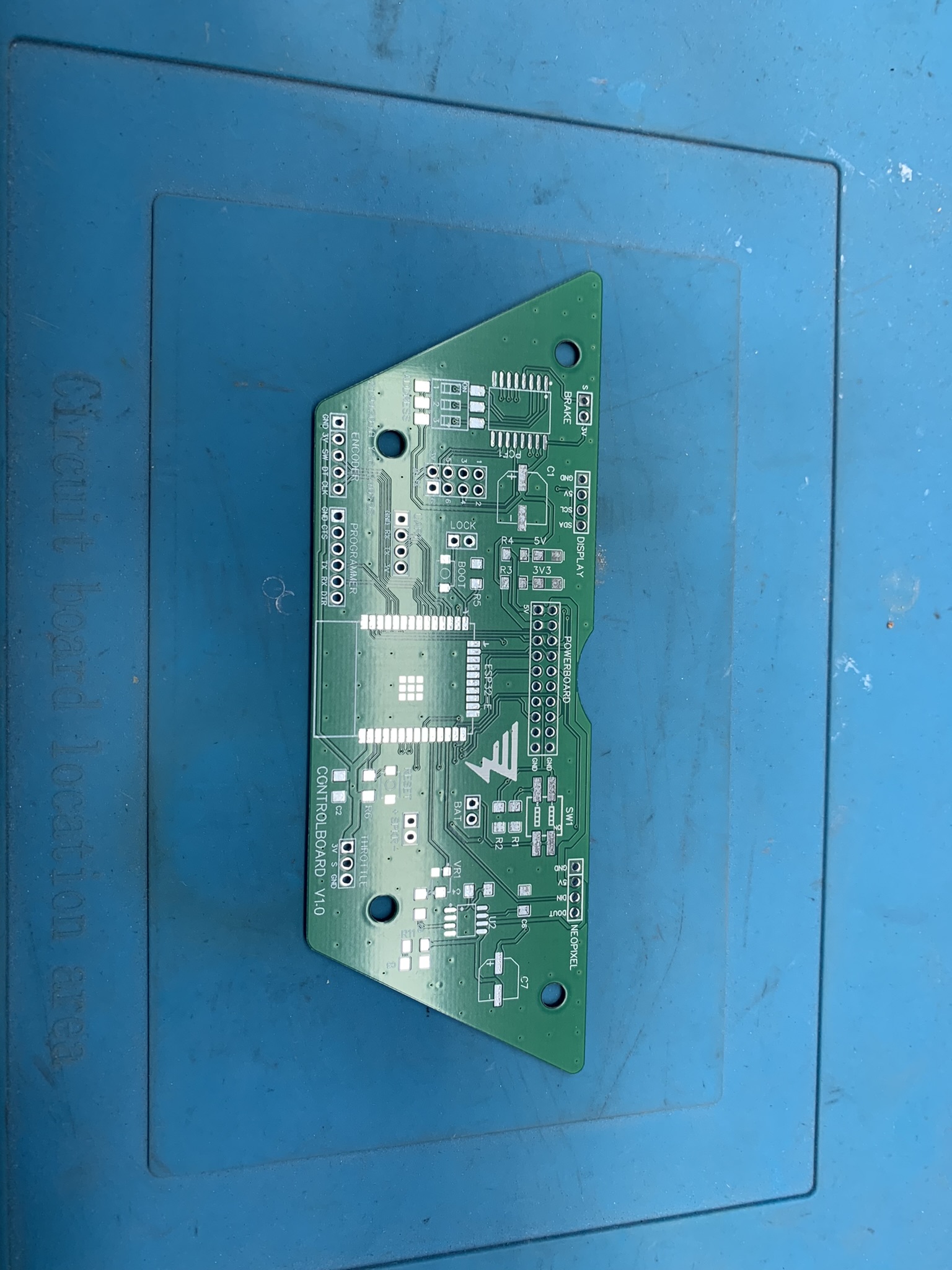
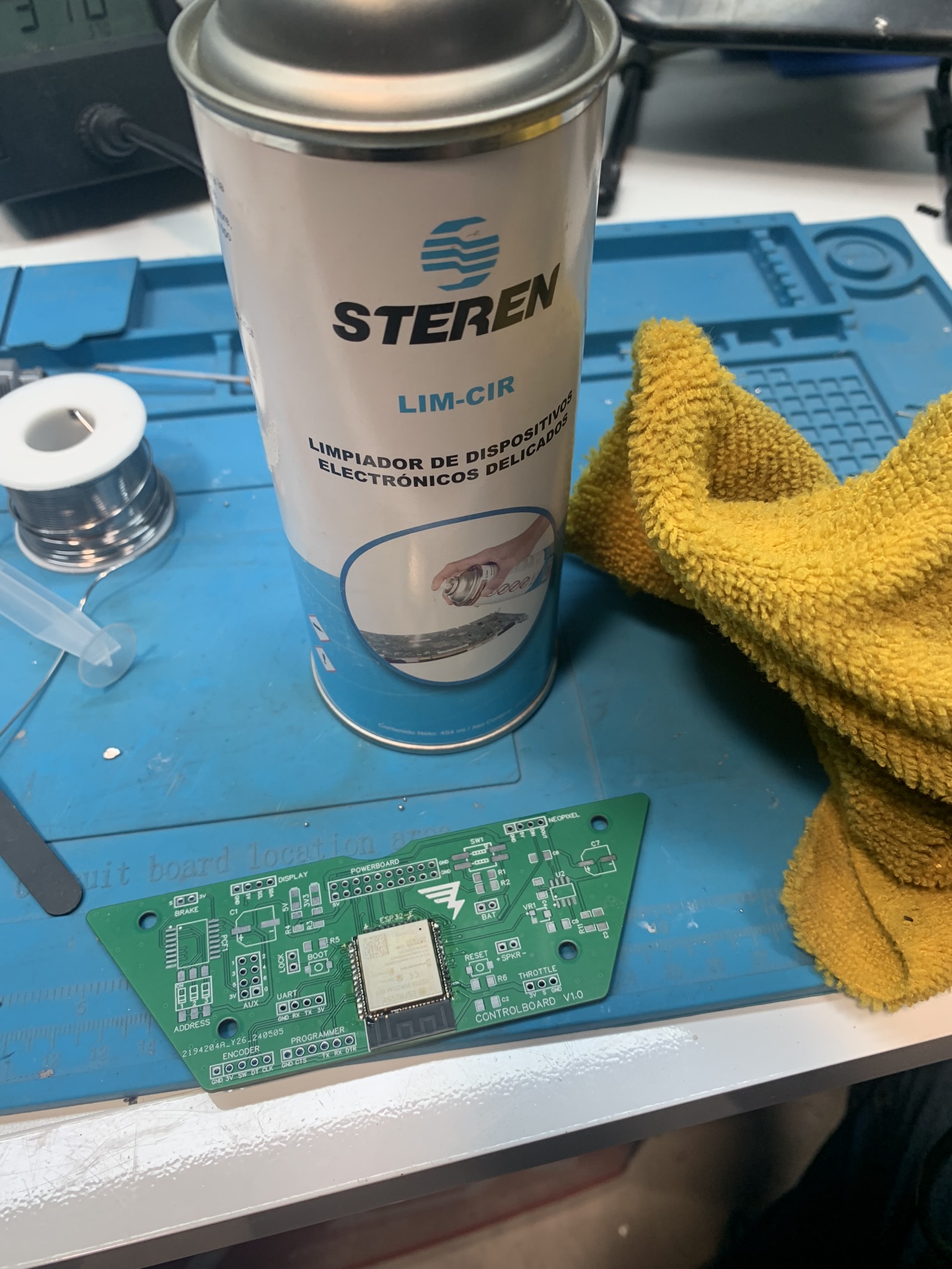
Then the next components are mounted, the smaller IC's and the resistors, LED's and capacitors follow. All through-hole components are left for last because soldering them at the beginning can make soldering other parts harder as they can get on the way.
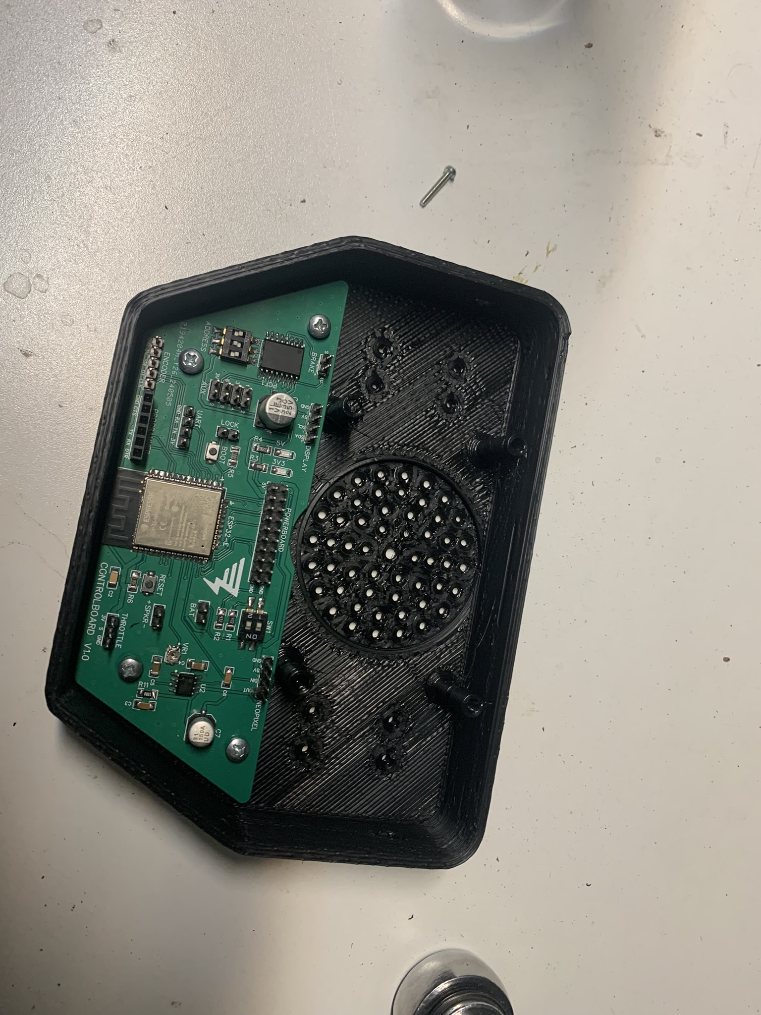
The finished board, fitted in its enclosure looks like this!
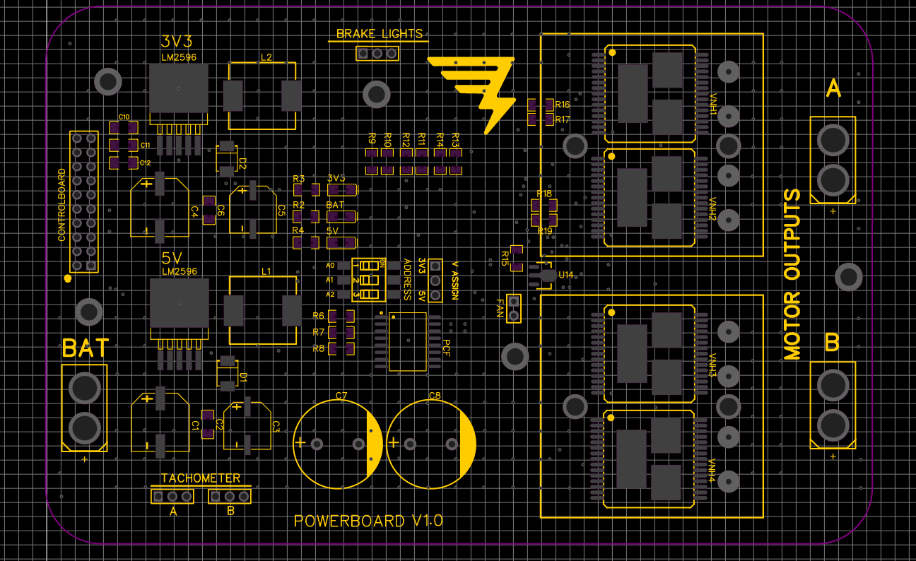
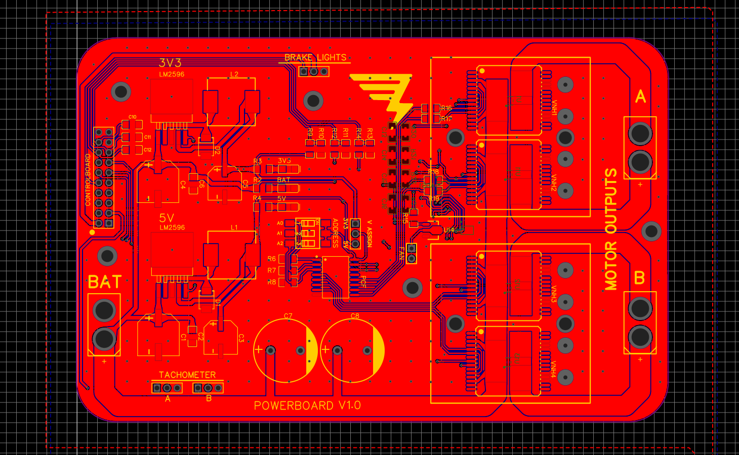
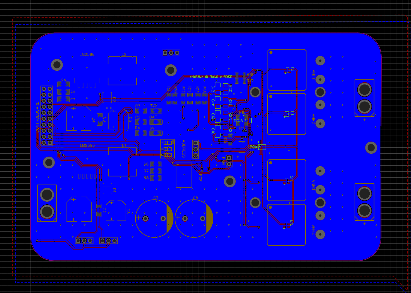
The Power Board:
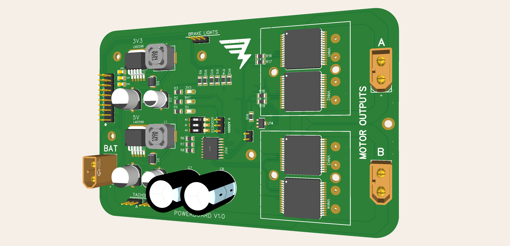
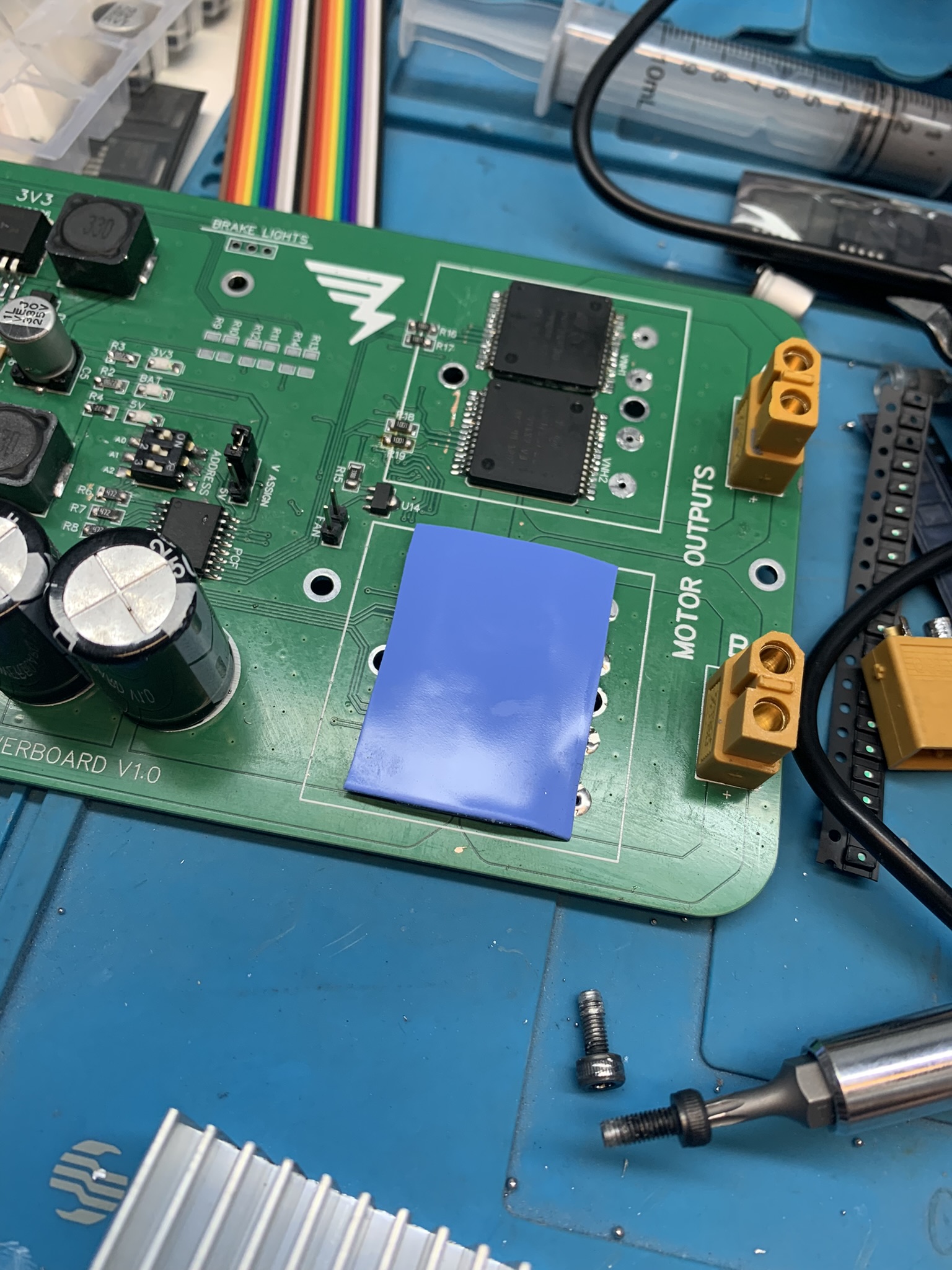
The power board is the more complex board of the two, and contains the following characteristics:
- Four VNH2SP30 high power H-Bridge IC's to control the motors.
- Two Buck Voltage Step-Down Converters to create 5V and 3.3V from the battery.
- A PCF8574 I/O expander to control the H-Bridges.
- Pin Headers for tachometers and brake lights.
- The same 20-way pin header connector for the flat cable that goes to the control board.
- A DC fan connector with speed control.
- XT60 connectors for the motors and battery.
- Mounts for 40x40mm aluminum heatsinks.
- Voltage divider sensor for battery voltage monitoring.
- Power LED's to show both 5V and 3.3V voltage rails are connected.
As the previous design I started with the component arrangement, leaving motor drivers in one side and beneath the aluminum heatsinks, and the voltage regulation circuitry on the other.
Within the design of the powerboard, power considerations become important, as both motors draw at least 20A of current during peak operation, so the width of the traces carrying that current should be calculated for optimal performance, if not, unexpected burnt traces may show up and destroy our board. Using THIS online calculator and inputting the current expected, the length of the trace needed (around 100mm), the thickness of the copper deposition on the board (1oz/ft2 in my case) and considering that the trace may "comfortably" heat up to a 100°C (only in prolonged max current draw which should never happen) the calculator gives out a value of 4.63mm width which I rounded up to 5mm. So you can clearly see, when the tracing is done, which are the power traces!
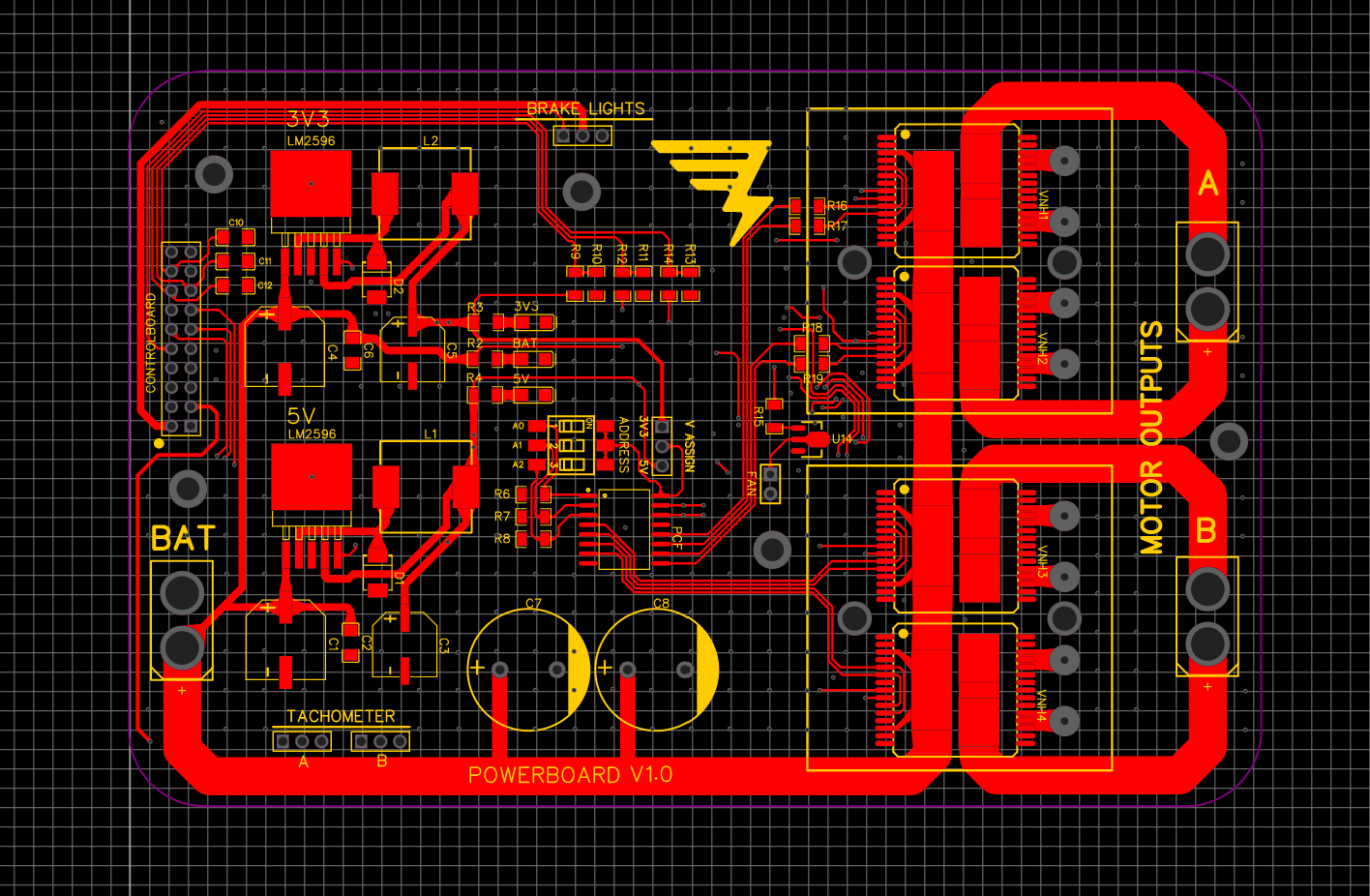
Teardrops are also used in this design!
Using a ground plane in this power-intensive PCB's becomes really useful to better manage the electromagnetic interference produced by the high currents of the motors switching on and off.
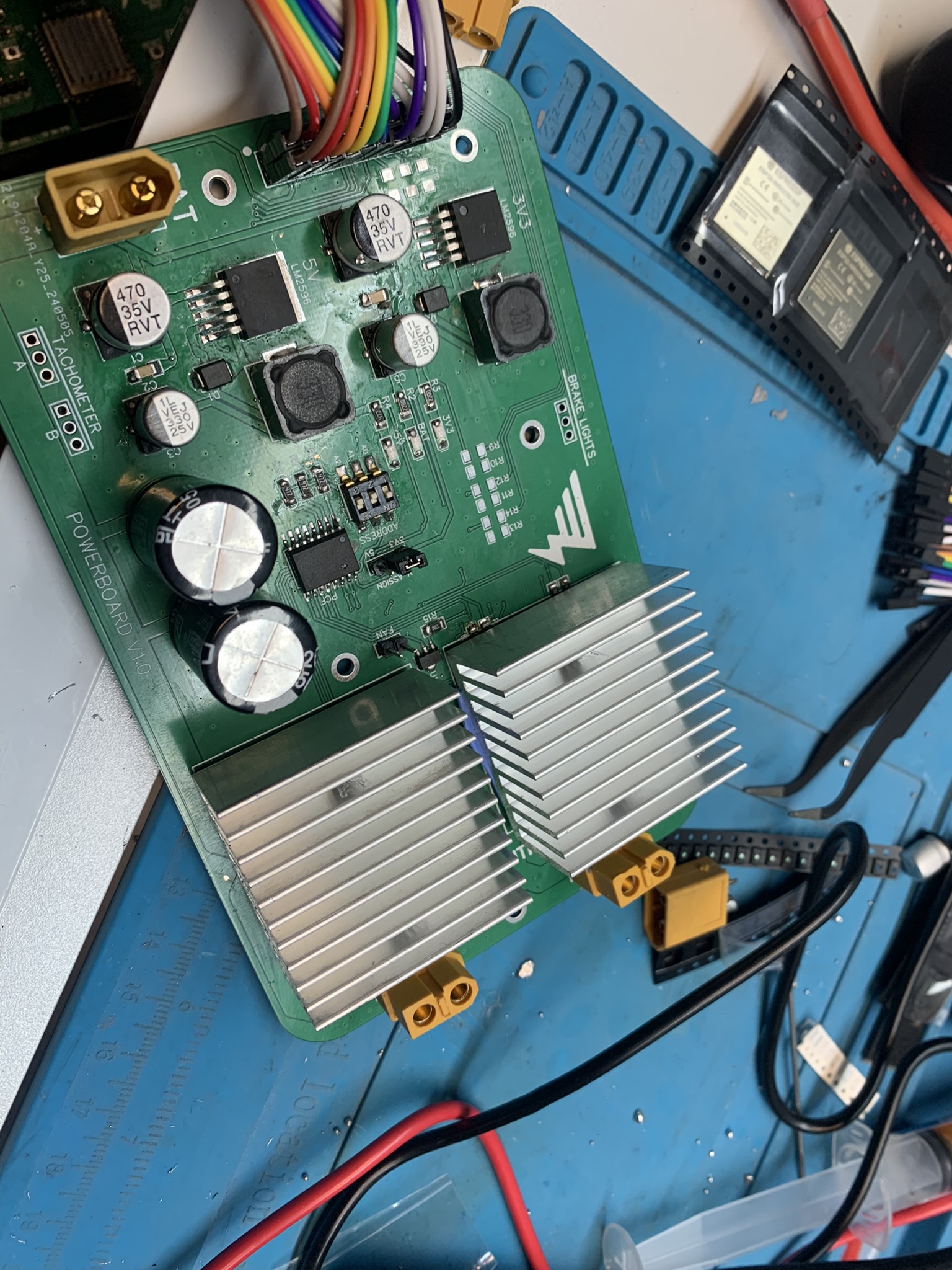
Soldering the Powerboard:
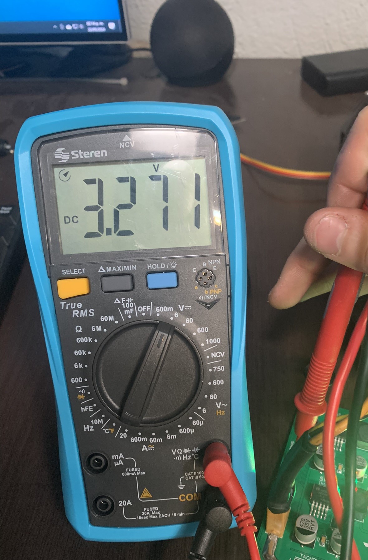
I followed the same procedure in this board as in the controlboard, first soldering the most heat intensive components, but this time, as the H-Bridge IC's were far from anything on the board, I left them for the end. I also soldered a single TH component: The battery XL60 connecto to check if the voltage regulators (the first circuit of the board I assembled), were working properly before even bothering to solder anything else.


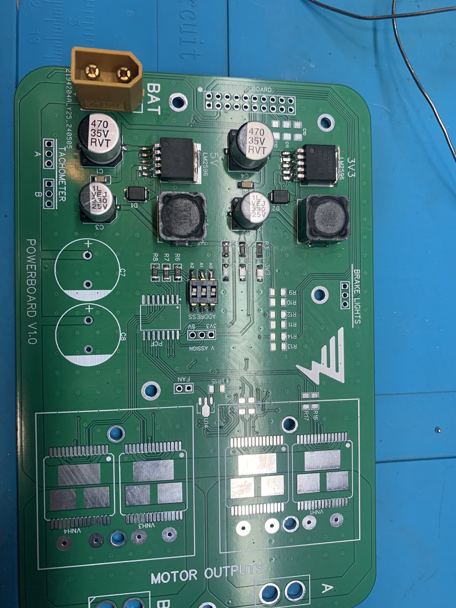
Here I am powering up the board using a small 12V battery with nothing else connected, to check using a multimeter if all the voltages are correct. And they were all right, measuring the expected 5V and 3.3V in the corresponding rails.

Then, I soldered everything else, including the VNH2SP30 IC's which handle the motors. These components need hefty cooling as they can get really hot during operation, so I contemplated a Heatsink mount for both arrays. A heat conducting pad was placed between the IC's and the Heatsink as a thermal interface. Finally the heatsinks were mounted using some M3 screws and its corresponding thread machined into the holes made in the aluminum.

And this is all for the electronics section! Please continue to the next section: Firmware Development
Download all final proyect assets here!