Even More COPPER
PCB Electric-Bogaloo!
You might remember we did a PCB board a while back. Now, it's time to design one PCB of our own, one of the things that is required to design such a thing is an embedded microcontroller, microcontroller is a small processing unit that does a lot of functions inside a circuit, it controls some of the behaviors the components might have, and it is used for programming the required instructions.
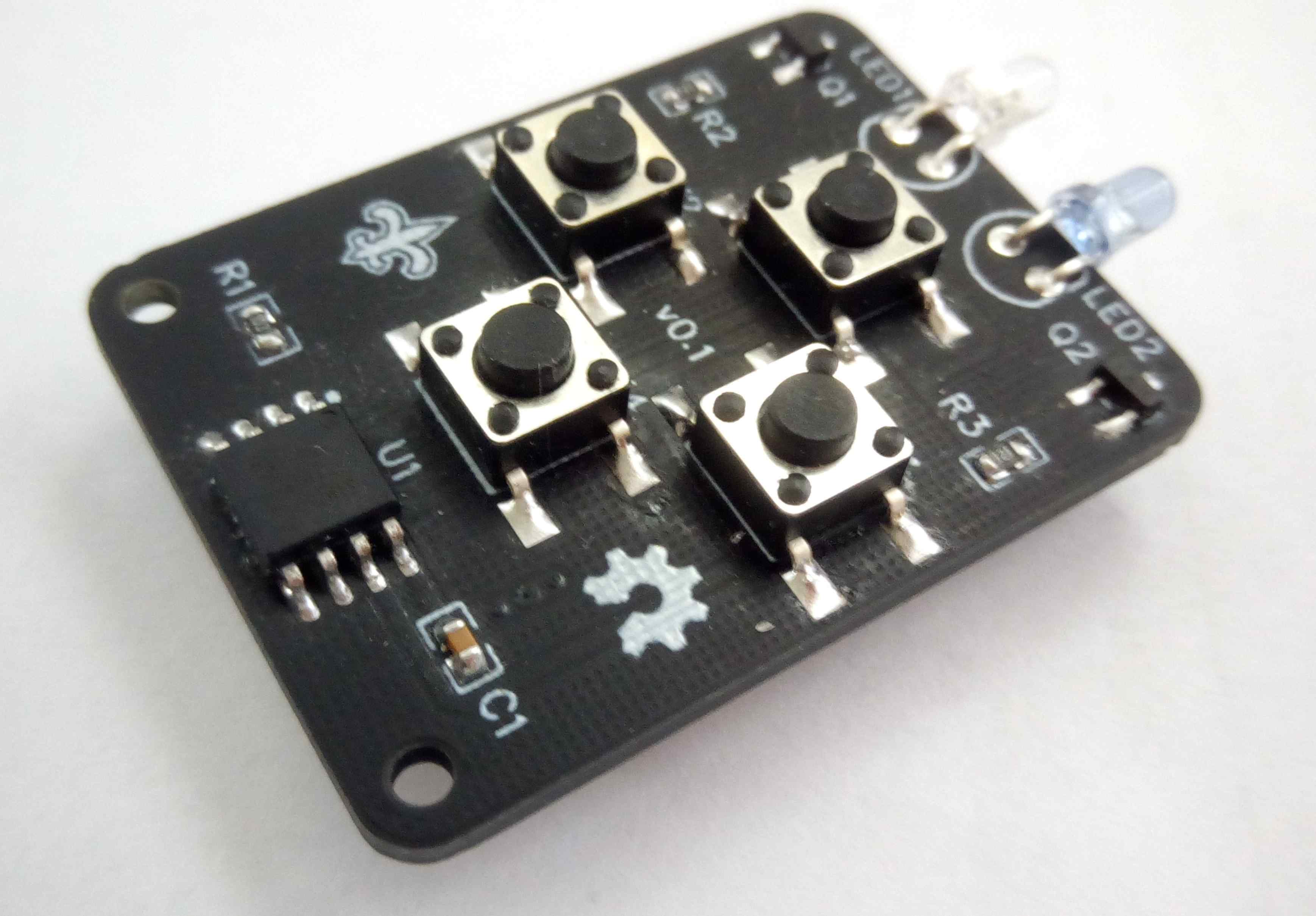
The first thing we need to do is to pick an idea of what to do, in my case I used an ATtiny 45 microcontroller unit to make a small SDM remote circuit, this is a basic circuit that would interact with buttons and LED diodes with a basic function, nothing too fancy, but I always appreciate the principle of component interaction and proper circuitry design. This idea comes from an EasyEDA user that made quite the controller, simple and effective, this is his finished product.
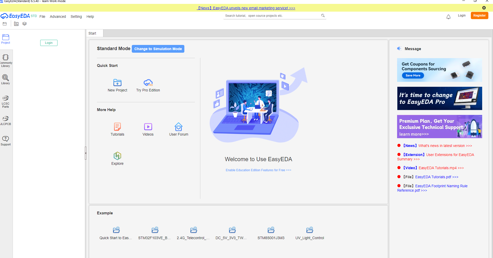
After getting the required idea we need to begin creating our design, for this we would need a PCB and schematic design software. There are many softwares to choose from such as: Altium designer, EasyEDA, Kicad, etc. I chose EasyEDA, which is a semi online design platform that interfaces with an actual market for real components that serve as reference to create our board. The first thing we need to do is create an account and install the software, then it's onto create a new project and assign it a name, this project will be saved online and will be added to the EasyEDA international project library, it's such a great feature as it allows you to access other people's projects for reference in case you're looking to create something similar to what somebody has already made.
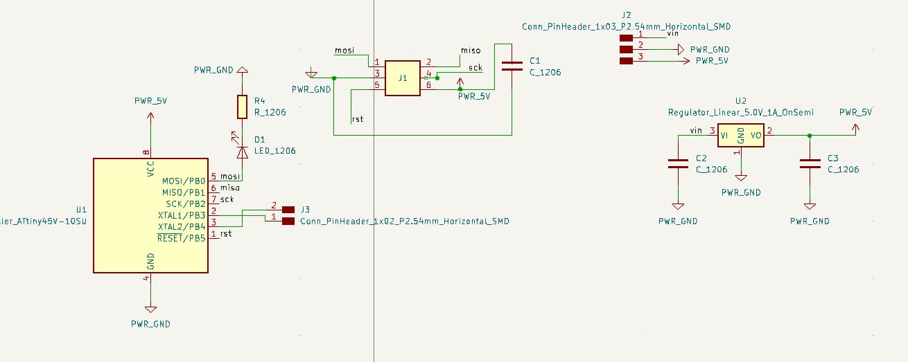
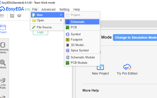
So, you have your newly created project, then we open the schematics tool, this is a section that is responsible for assigning the connections to the different components that will be included in our circuitry. We can notice the workspace and several different tools that are located throughout the screen. The tool that serves us the most is the common library and the library sections; this is the place where we can find all the components that we might need to create our PCB board. In my case I search for an ATtiny 45 processing unit, to LED diodes, two npn bipolar transistors, five buttons, two 120-ohm resistors, an 100nF capacitor, and six 0-ohm resistors, later on, I will explain the why in using 0-ohm resistors. And by meaning later on I mean right now: so, those 0 resistors are there for a reason, this being that there are certain connections between components that, when the time to design the PCB footprint and layout, will present some challenges in routing and effectively connecting each other as is required, so, this resistors are there to serve as bridges, letting the voltage through otherwised blockaded areas of the PCB while leaving the rest of the routes without disruption.
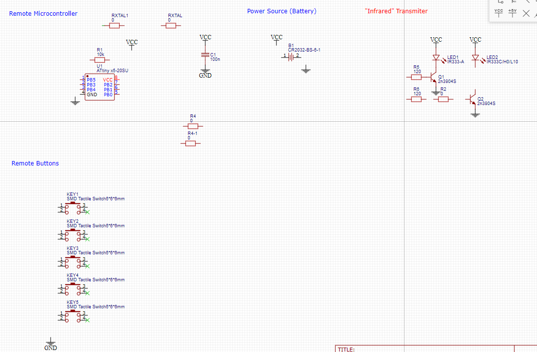
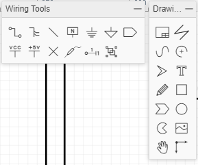
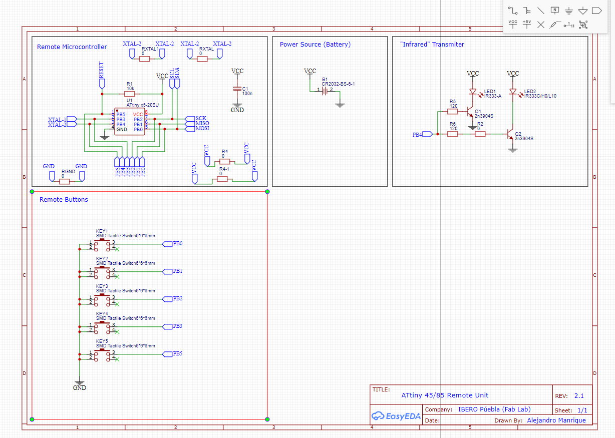
Now that we have all our components arranged in our schematic we need to begin with the necessary connections, this is done in order to tell the software which component will be connected to which other components so thatwhen it comes to the part of actually designing our PCB layout, the software will automatically tell us which connections are to be done when we begin making the routes. But first we need to wire the system, this is done by using the wire to and connecting the components from one end to the other in the correct order. Another tool you might find useful if you despise seeing all those complex web of connections and wires is the "net label" tool, this stands for a label that is placed in one end of a component that shares the name of another label that you might insert in another component so that the software automatically knows that any component with that same label is connected in the network. Other tools you might find useful are the text to which allows you to tell the user which section of your circuit is which, as well as the shape drawings section which allows you to draw rectangle such as the one I have to separate all of the parts of our board to create a clean distinction of between each component.
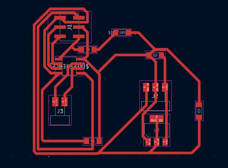
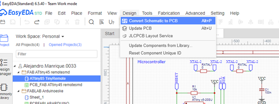
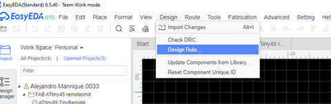
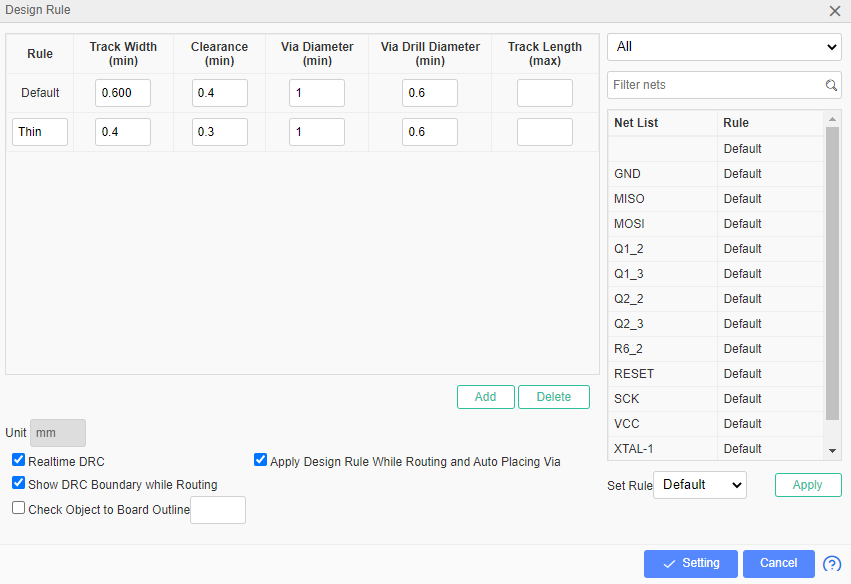
Then, after having done all the schematics, we save the document and we create a PCB design file. Then, we import all the schematics into that design file to get all of the footprints of the components(representation of what space the component takes up in the actual PCB design layer) into the layout. We then arrange the components into a way that the connections are not as badly distributed, and we begin with the routing process. Routing is done to create a sort of highway of energy that is delivered amongst different components for them to work in our circuit. In in my case, my route is 0.6 mm wide with us 0.4 millimeters spacing in between each route, does design rules are made because of my milling and drilling diameters within the machine I'll be using to create the board. Mind you, some sections of the routing part might be thinner than others, that's because of the spacing limitations between the routes, as 0.6 mm might be too much on certain heavily invested routing areas.
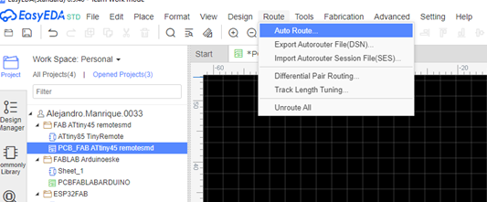
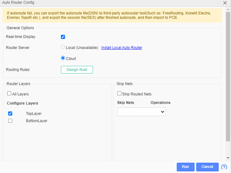
There are two choices in the EasyEDA software when it comes to routing: Doing it manually or using the automatic routing tool to give you a sense of how the circuit needs to be distributed in order to make the least amount of connections, this automatic tool is not perfect but it's quite useful to know if your design is actually able to get all the connections in place.
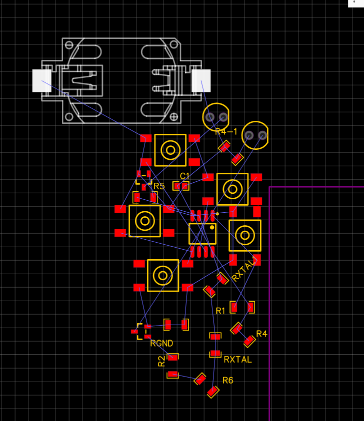
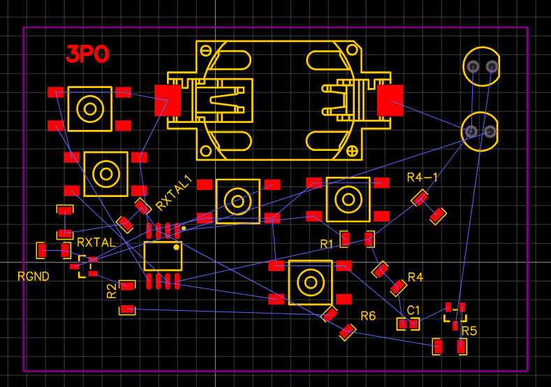
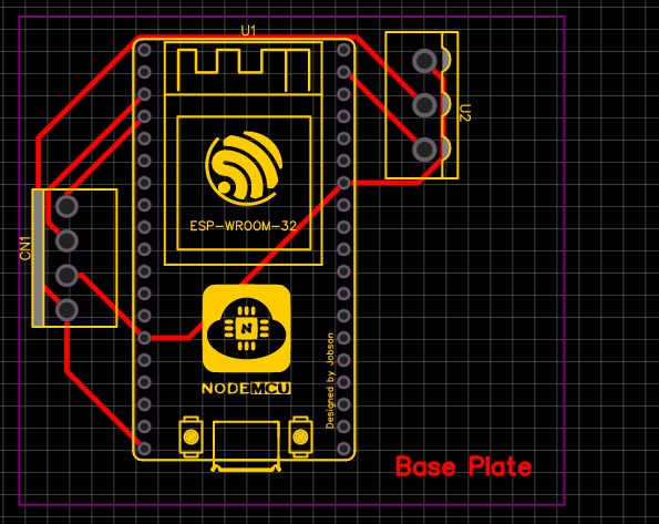
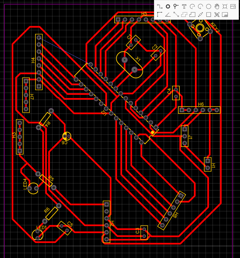
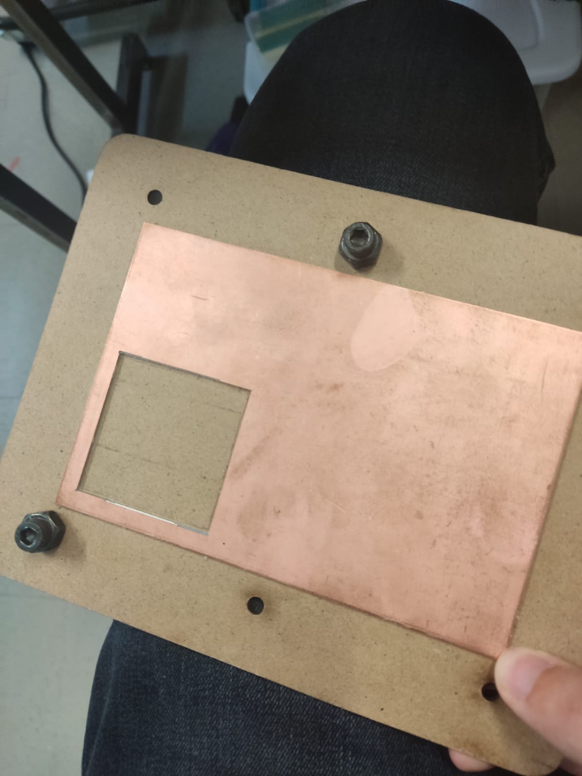
There are different designs you can adopt in a PCB board, but mine is a single layer no-hole layout, this is done due to the limitations in the machine I will be using in the facilities of the university, and the no-hole rule is due to the Fab Lab regulations. One of the things I noticed while making the design is that I was troubled with the number of components that can be used in the PCB design. What I'm trying to say is that the currently established controller is my fifth attempt at designing a PCB board, as the other previous attempts were met with failure due to the regulations made by The Fab Lab and the limitations of the university's machines. So, by the end, things were a little frustrating, but it's all part of the process. Here are some pictures of the previous iterations of my designs.
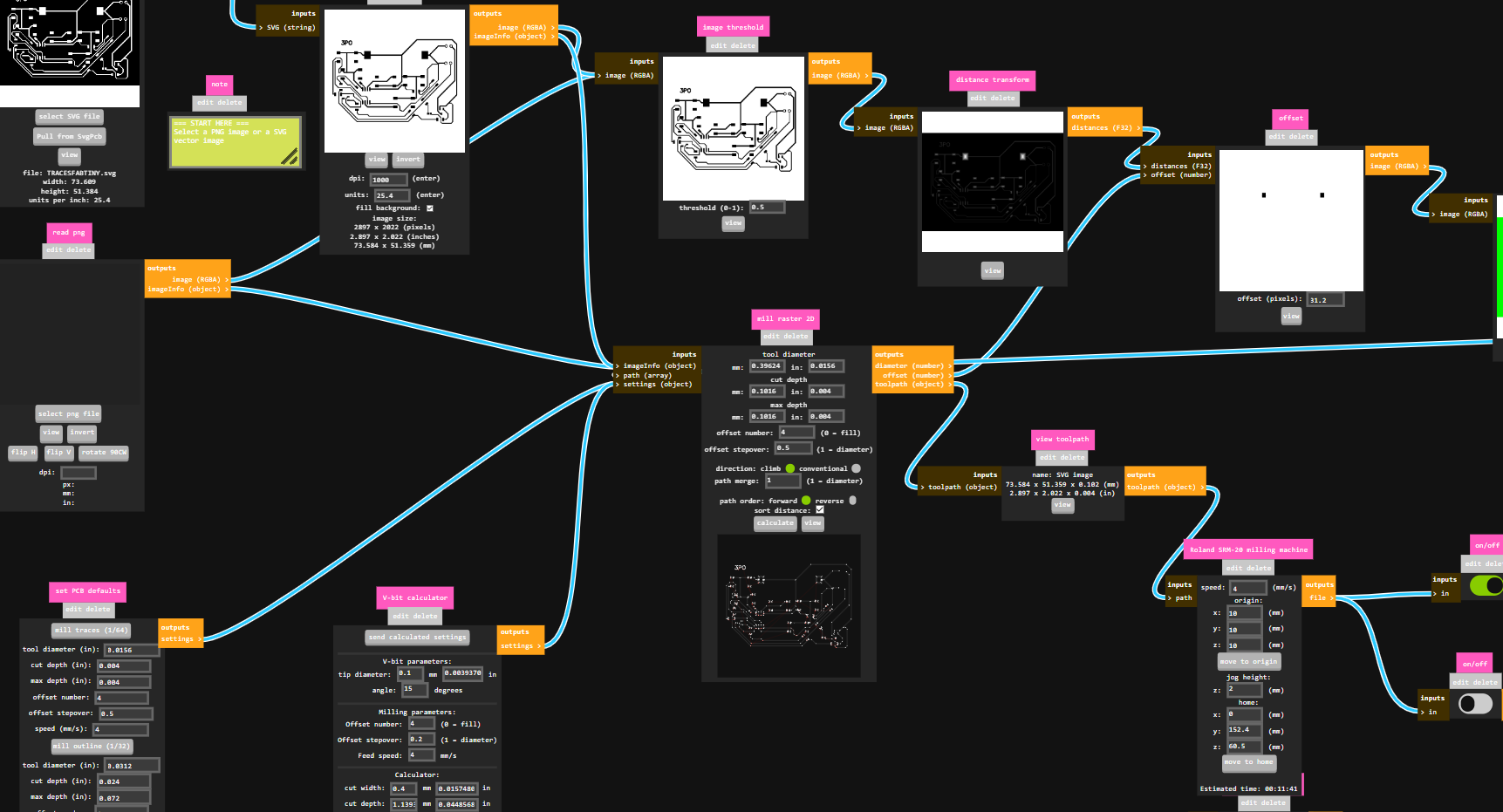
So, this is the final design I'll be using in my PCB board. The next thing to do is to export our design in the file extension that we need to use the mods platform. Now if you remember, this was a platform we used back when we made that previous RP2040 PCB board. We load up the file, use the correct color scheme: black and white coloring, and we modified the necessary stats to adjust them to the machine, after that's done is just a simple click in the calculate section in the middle so that we can download our g code that's loaded within the .rml file that the website gives us.
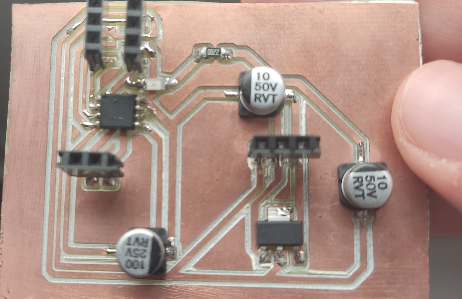
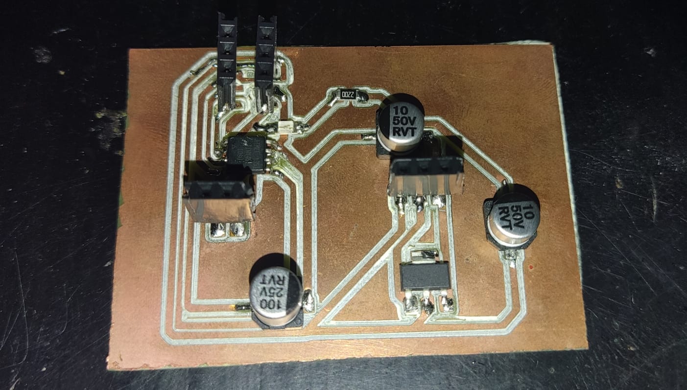
Finally, a quick trip to the Roland SRM-20 milling machine for PCB design, other use of the V panel to establish the origin points and loading the G-Code to begin the cutting and tracing process. Sadly, after three different attempts, I wasn't able to complete this week's assigment on schedule, there were several complications surrounding the machines I was using as well as not enough time for everybody to perform the necessary processes, then, when I did have an opportunity to cut and trace a copper plate, it didn't turn out in the way it was supposed to be, it actually flipped the tracing instructions and did an outer tracing process by marking the outside of each route. But don't you worry, I will keep at it as soon as I have the time to complete the task as it was meant to be completed.
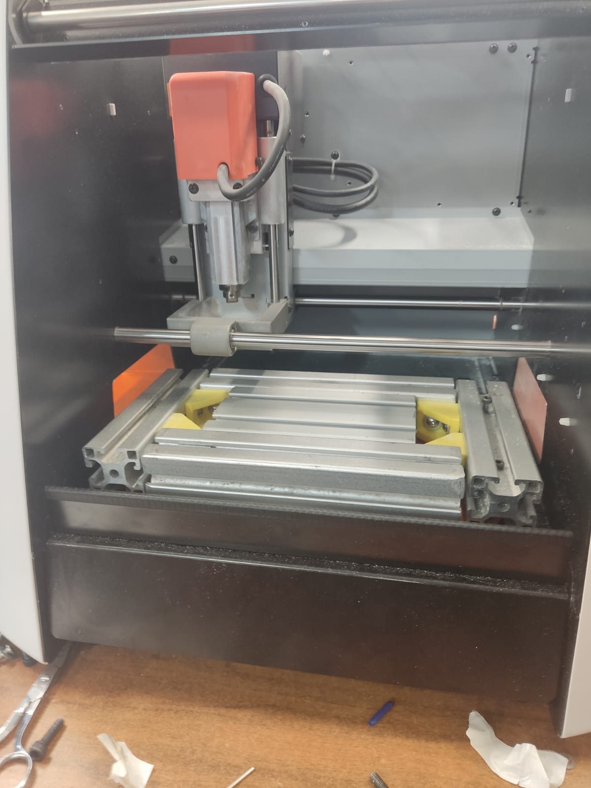
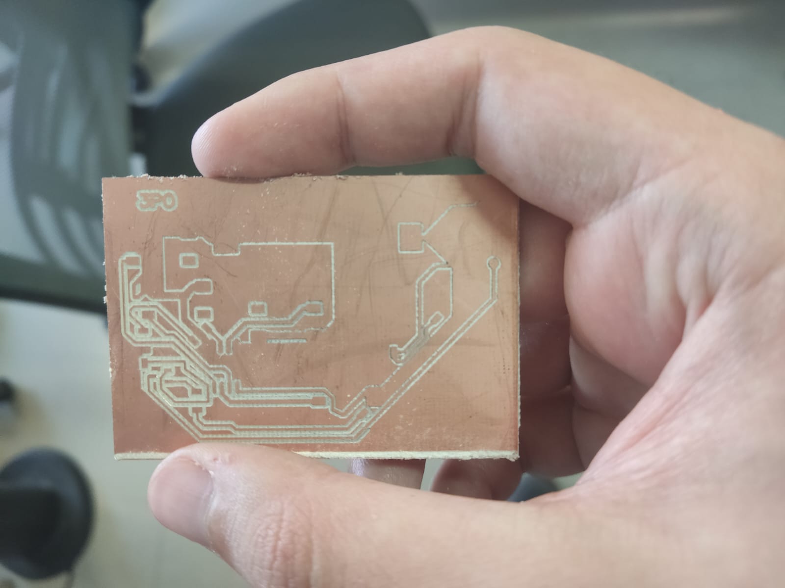
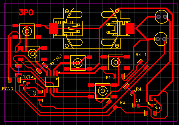
Well, I said that I was gonna complete the assigment whenever I could and here I am! I got this new and improved design using a ATtiny45 still, but with the idea of using a buzzer for the Output assignment week, here are the schematics and the PCB route, for the outcome and further explanation head to the Output devices week.Here is also how it ended after the milling machine and the soldering. Also, here's the component list for said board.
- 1 220 SMD 1206 Resistor
- 1 ATtiny 45 MCU
- Female Pin Headers
- 1 AMS 1117 SMD 5 V Regulator
- 1 100nF Capacitor
- 2 10nF Capacitor