Electronic Desing
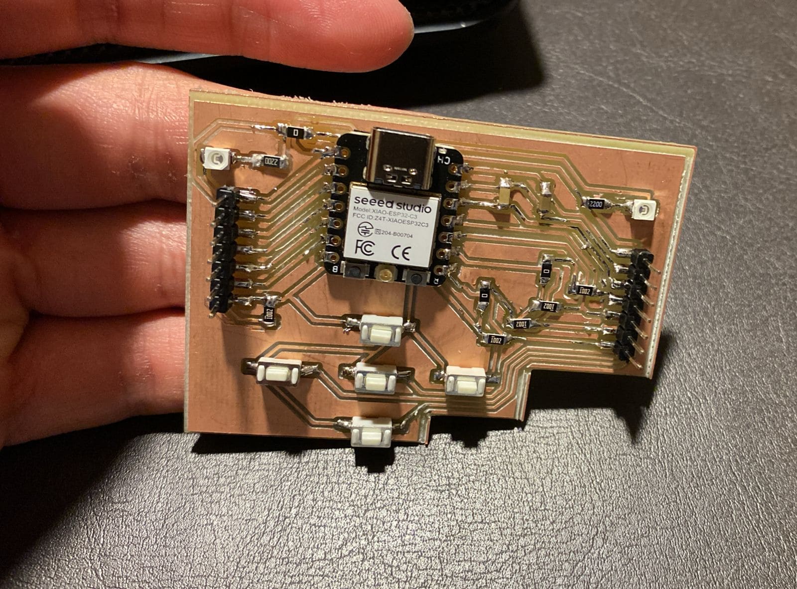
This week focused on creating a custom PCB design using KiCad, an open source software. I decided to design like a controller with buttons and LEDs to convey different sequences, such as waiting, winning, or losing. Let's dive into the process. Let's jump right into the process of making this PCB.
KiCad
KiCad is a powerful open-source software tailored for PCB design. It offers a comprehensive suite of
tools and a user-friendly interface, making it ideal for both beginners and experienced designers. To
kickstart your PCB design journey, all you need to do is download KiCad from its official website or
through the provided link.
Schematic
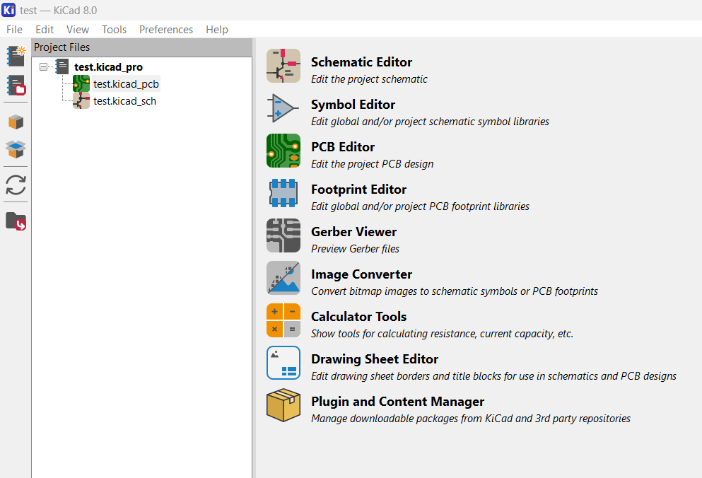
Upon launching KiCad, you'll see some prominent icons on the right side, offering access to key tools. I mainly used the schematic editor and PCB editor. Clicking on the schematic option opens a window with essential tools for adding components. This straightforward interface simplifies the process of creating your schematic layout, setting the stage for further PCB design.
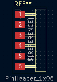
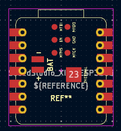
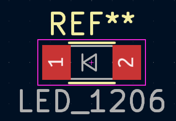
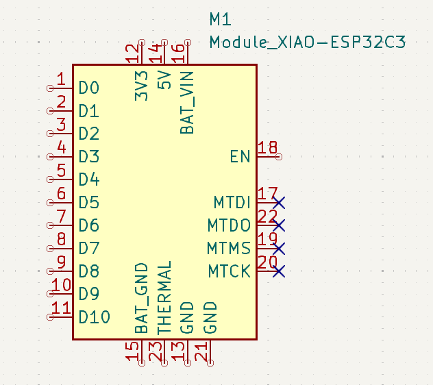
To access symbols in KiCad, navigate to the right sidebar and select the third option or press "A". This action opens a new tab displaying default symbols, which offer a comprehensive selection. However, I opted for the Fablabs library provided in class, which better suited my needs. From there, I selected the components listed below.
| Name | Quantity | Symbol | Footprint |
|---|---|---|---|
| Push button | 5 | 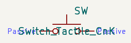 |
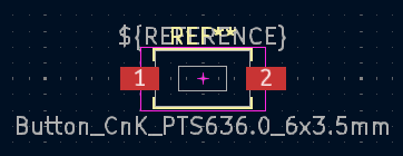 |
| Resistor 1206 | 10 | 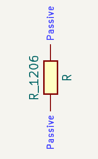 |
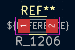 |
| Capacitor 1206 | 2 | 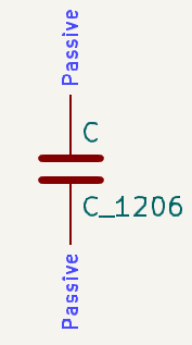 |
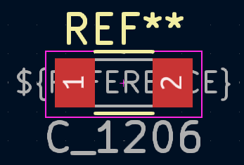 |
| Male SMD pins | 14 | 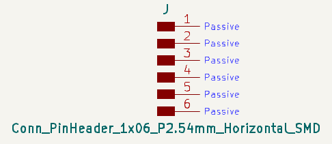 |
 |
| Xiao ESPC3 | 1 | 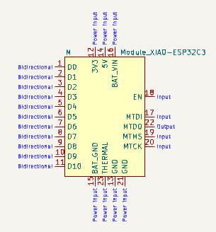 |
 |
| LED 1206 | 2 | 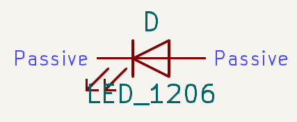 |
 |
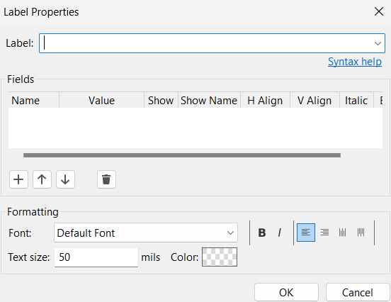
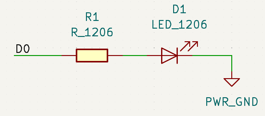
To connect components with wires in KiCad, click on the fifth icon on the left sidebar or press "W". If components are in difficult positions, you can rotate them by selecting the component and pressing the letter "R". Labels are also helpful for organization. You can access them by clicking on the tenth icon or pressing "L". A menu will pop up, allowing you to write the type of label you want. In my sketch, I used labels like "D0" to denote specific connections.
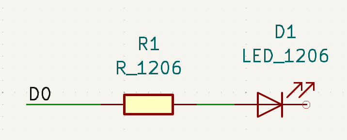
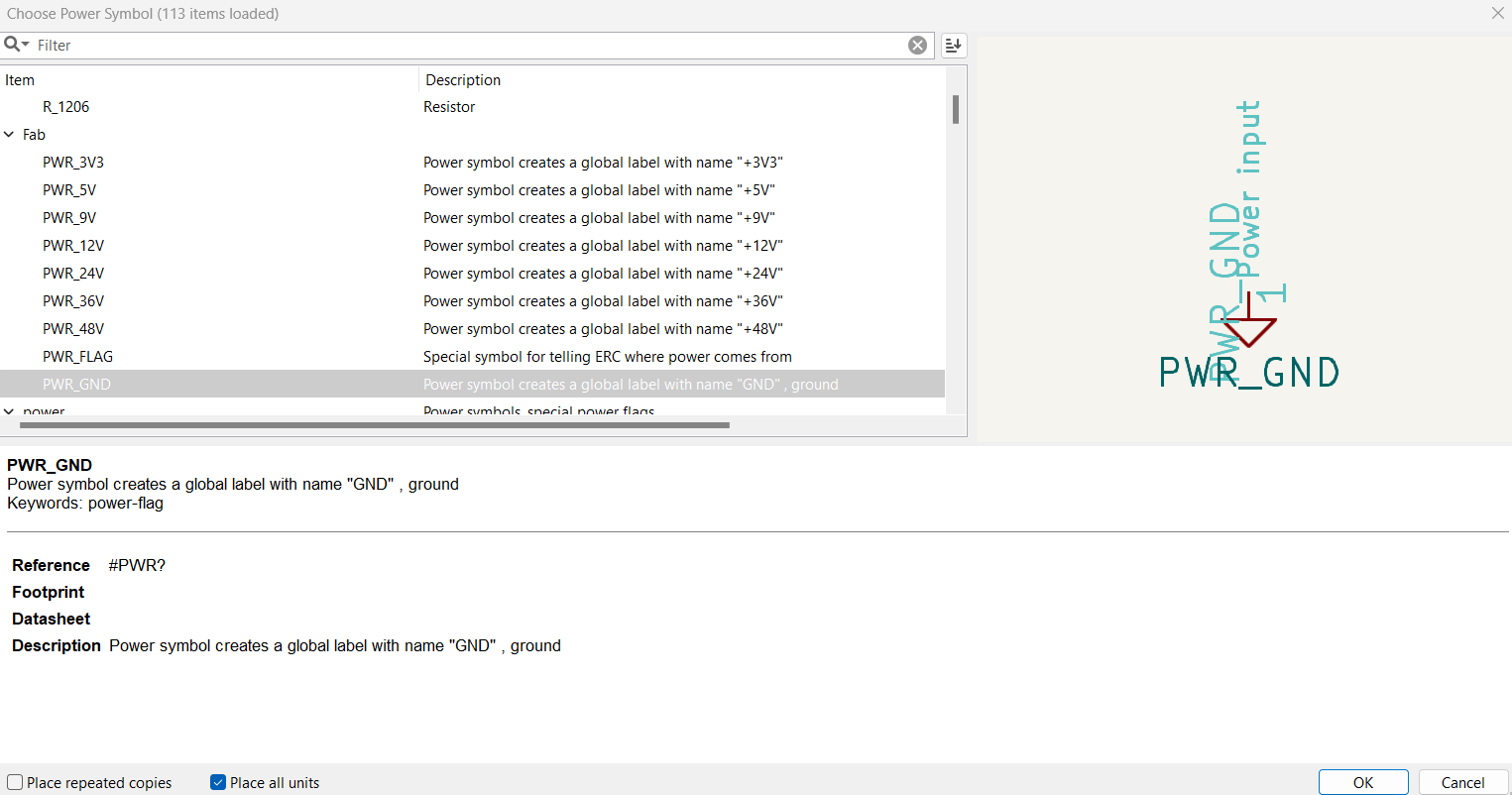
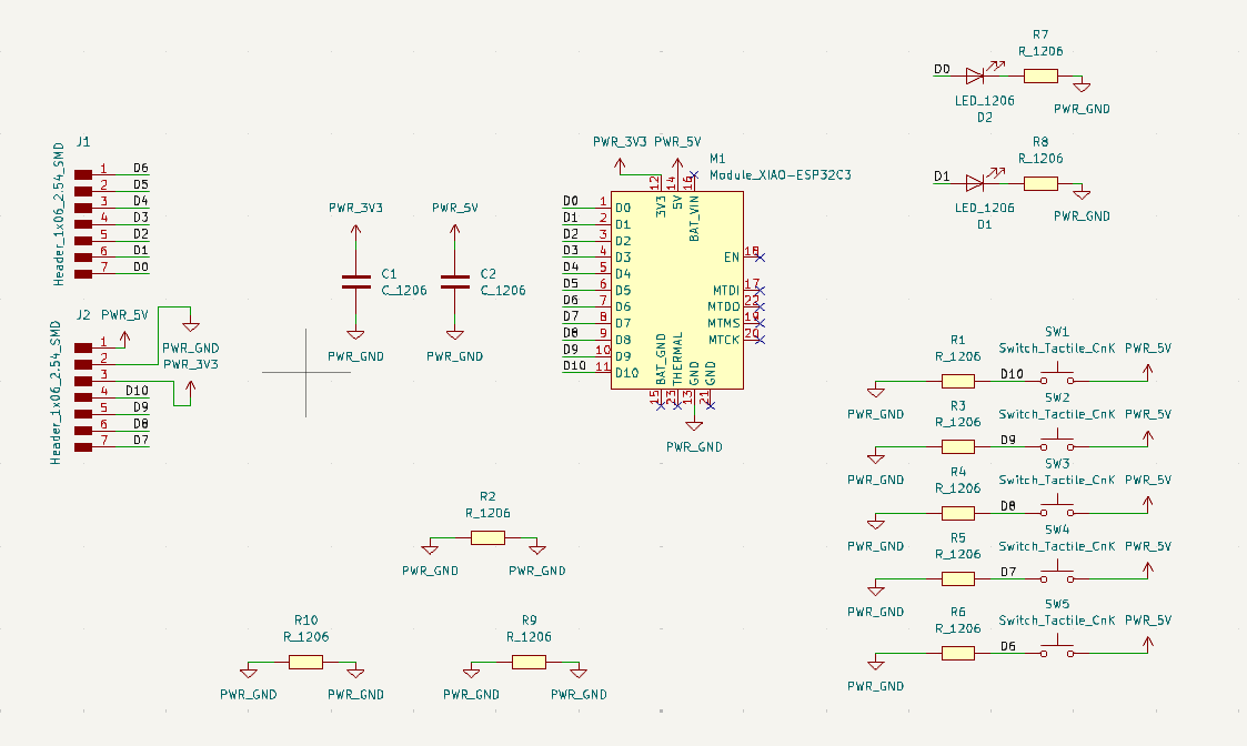
For connecting the power supply symbols, you can use the 4th icon or press the letter "P". A menu will pop up, similar to the symbols library. You need to find the ground and voltage symbols. In the Fab library that I used, I selected symbols like PWR_3V3, PWR_5V, and PWR_GND. Add one of these symbols to the specific pin as shown in the schematic.
Additionally, the "draw no connections" flag is useful for indicating unused pins; you can access it by clicking on the eighth icon or pressing "Q". With these tools, you can easily follow the schematic layout.
PCB editor
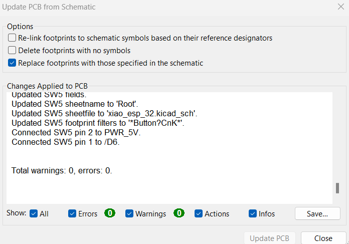
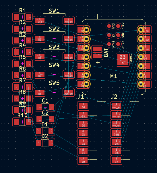
Once you have all the connections on the schematic, it's time to place the components in the right positions on the PCB To do this, open the PCB editor. To import the components from the schematic, go to the top bar and click on "Tools". Select the option called "Update PCB from schematic", or you can press F8. Then, click "Update PCB". Close that window, and you'll have all the components available. Place them in positions where you think you won't have any problems connecting them.
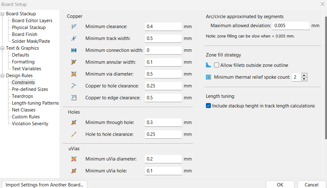
Before connecting all of the components, you'll need to establish some design rules to ensure proper
fabrication. These rules dictate the minimum clearance and track width to prevent issues during
manufacturing. To set these rules, navigate to "File" and then click on "Board Setup." In the menu
that appears, go to "Design Rules" and then "Constraints." Here, you can specify parameters such as
the minimum clearance and track width. For example, in my case using the Roland SRM-20, the minimum
clearance is set to 0.4 mm, and the minimum track width is 0.5 mm.
After setting up the design rules, you can begin connecting all the components. To do this, click on
the fourth icon on the right sidebar or press the letter "X" to initiate the connection tool. Then,
select one end of a component and connect it to the other end. The software will assist you by
displaying the quickest path for the trace. Make sure you allocate sufficient space to avoid missing
traces, as cramped layouts can hinder proper connections.
The resistors connected to the same line in the schematic are known as "resistors with 0 ohms." These
components are valuable when designing PCBs with only one layer because they effectively act as extra
traces. When aiming to minimize the size of a PCB and facing space constraints, these 0 ohm resistors
offer a convenient solution by serving as additional pathways. This is just one of the applications
for 0 ohm resistors, and further exploration can reveal more uses for them. Feel free to follow the
connections I've made in the design, or if you prefer, you can rearrange them according to your
preferences.

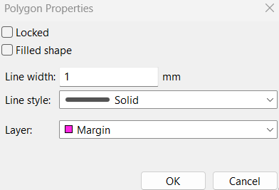
The final step involves adding a margin to the PCB design, which is crucial for determining the cutting boundaries. Begin by selecting the margin layer and using the drawing tools located in the right sidebar to create a perimeter that enclose all the components inside. Once the perimeter is drawn, double-click on the margin to adjust its properties. Set the line width to 1 mm, as this matches the thickness of the cutting tool used in the Roland SRM-20. With the margin in place, your PCB design is now ready for fabrication.
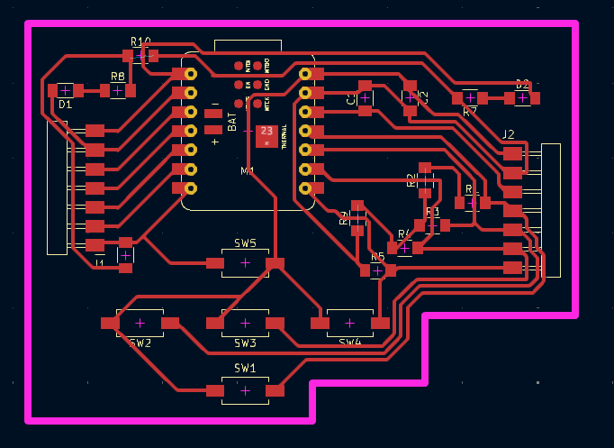
Export the PCB design as SVG files. Start by exporting the copper traces layer, ensuring that the print mode is set to black and white and the board area only option is selected for the SVG page size. Next, export the margin layer as an SVG file with the same settings. Process the SVG files into G-code files using "mods" page. Once processed, you can load the G-code files onto your CNC machine for fabrication.
Soldering and testing
After manufacturing the PCB, the next step involves adding the components, which are consistent with those listed in the schematic. However, there are minor adjustments to consider, particularly with the resistors and capacitors. While the schematic specifies the sizes of these components, it's important to note that for resistors, there are 5 10k ohm resistors for the pushbuttons, 2 220 ohm resistors for the LEDs, and 3 0 ohm resistors, typically used as jumpers. As for capacitors, two 1uF capacitors are required.
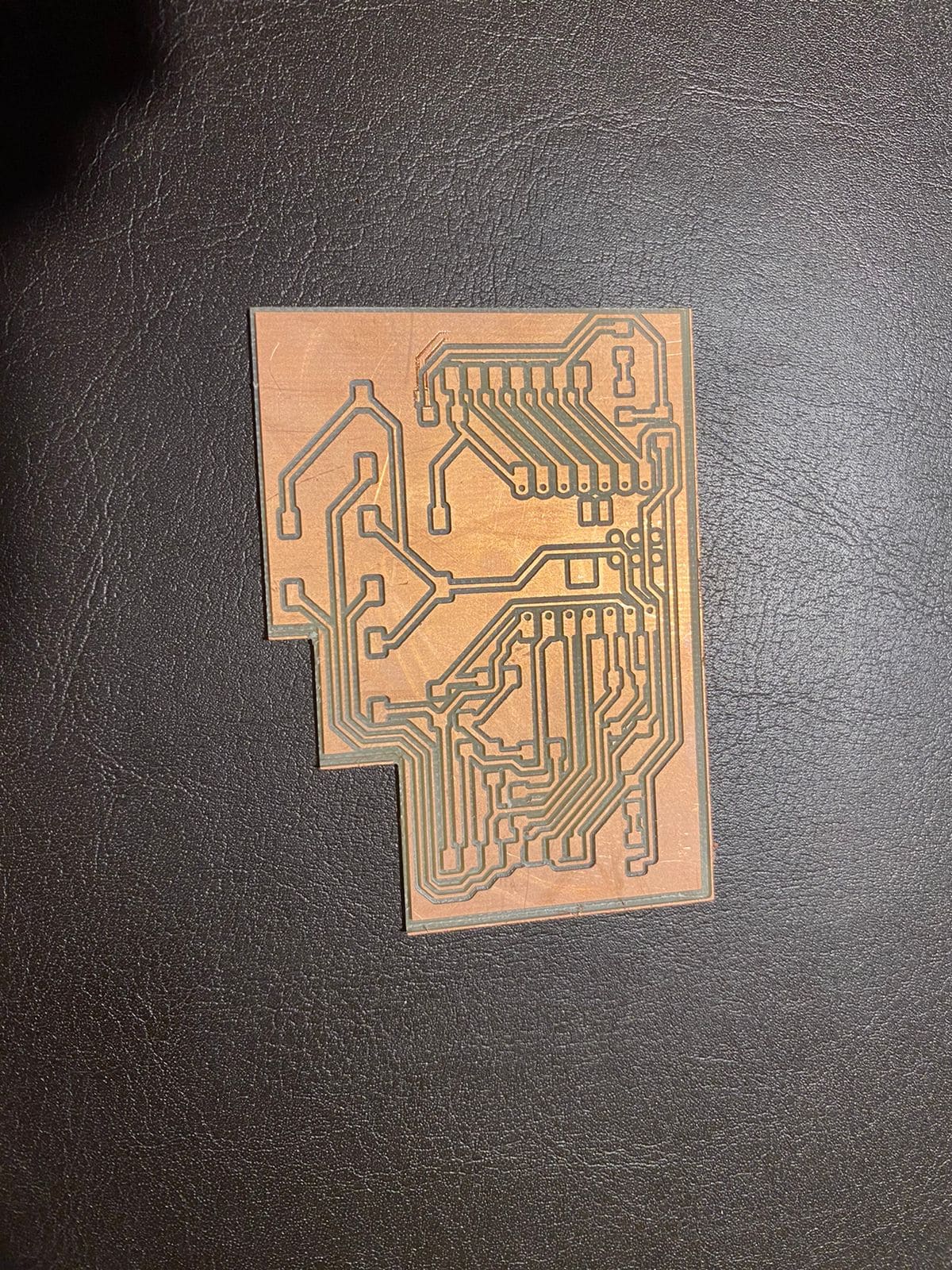

To test the PCB, upload the Tetris sketch from Arduino. This code is readily available on a webpage that provides detailed information about the game. You can access this page by clicking here.
Group assignment
This week's group assignment focused on testing the PCB using an oscilloscope and a multimeter, aiming to assess various outcomes for different microprocessors such as the Xiao or the ATtiny. The objective was to gain a deeper understanding of these valuable resources and their functionalities. For further insights into this topic, you can access the detailed information provided in the assignment by clicking here.
