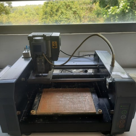
In PCB production at fab labs, we employ the milling machining method, akin to printing on paper with a regular printer.
The fab lab offers a Roland MDX 20 3-axis milling machine for this purpose.
This machine functions as a standard milling machine suitable for PCB fabrication.
What is PCB?
PCB stands for Printed Circuit Board. It is a thin board made of non-conductive material (usually fiberglass or composite epoxy) with conductive pathways printed or etched onto its surface.
These pathways, typically made of copper, provide connections between electronic components like resistors, capacitors, and integrated circuits.
PCBs are essential components in almost all electronic devices, serving as the backbone for electrical connections and ensuring proper functioning of the circuitry.
They are used in everything from smartphones and computers to household appliances and automotive systems.
FR1 PCB
FR1 PCB refers to a type of Printed Circuit Board (PCB) material.
FR1 stands for "Flame Retardant 1." It is a type of paper-based substrate that is impregnated with a flame retardant resin, typically phenolic resin.
FR1 PCBs are low-cost and have good electrical insulation properties, making them suitable for various applications such as prototyping, hobbyist projects, and low-frequency electronic circuits.
However, they are not suitable for high-frequency or high-power applications due to their limited thermal and mechanical properties compared to other PCB materials like FR4 (Flame Retardant 4).
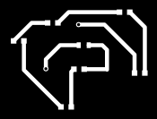
Quentorres board
The Quentorres board, initially conceptualized by Quentin Bolsée, underwent a significant redesign spearheaded by Adrián Torres in 2024 during the Instructors Bootcamp held in León.
This revamped iteration of the board boasts versatility, specifically tailored for programming both AVR (Automatic Voltage Regulators) Series 1 and 2, along with ARM (Advanced RISC Machines) microcontrollers.
Equipped with fundamental input-output functionalities such as buttons and LEDs, it also incorporates breakout pins facilitating seamless integration with external components.
Roland Modela MDX20
The Roland Modela MDX-20 is a compact desktop milling machine ideal for rapid prototyping and small-scale production.
With 3D milling capabilities, it can precisely shape various materials like wood, plastics, and non-ferrous metals.
Equipped with user-friendly software, it facilitates easy design creation and toolpath generation.
Its versatility extends to compatibility with standard CAD/CAM software.
Some models feature an automatic tool changer for efficiency in complex designs.
Popular in industries like product design, engineering, and education, the MDX-20 offers a convenient solution for creating intricate prototypes and models with high precision, making it a favored choice for diverse applications.
More details are available here.
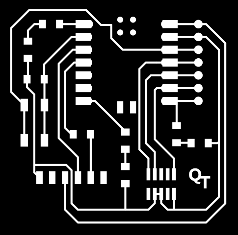
Board personalisation with GIMP
During the second week, I learned to use GIMP. I used it to make the board unique, adding my name to it.
So I downloaded the files and opened it in in GIMP.
Next, I tried to remove QT and added my name Thej.
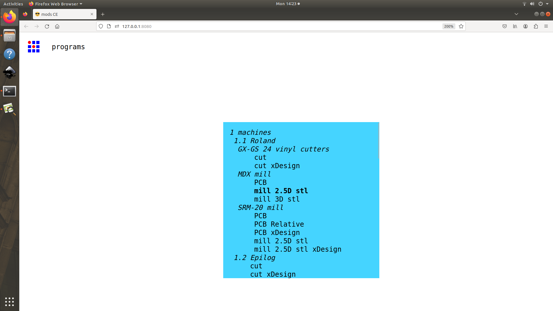
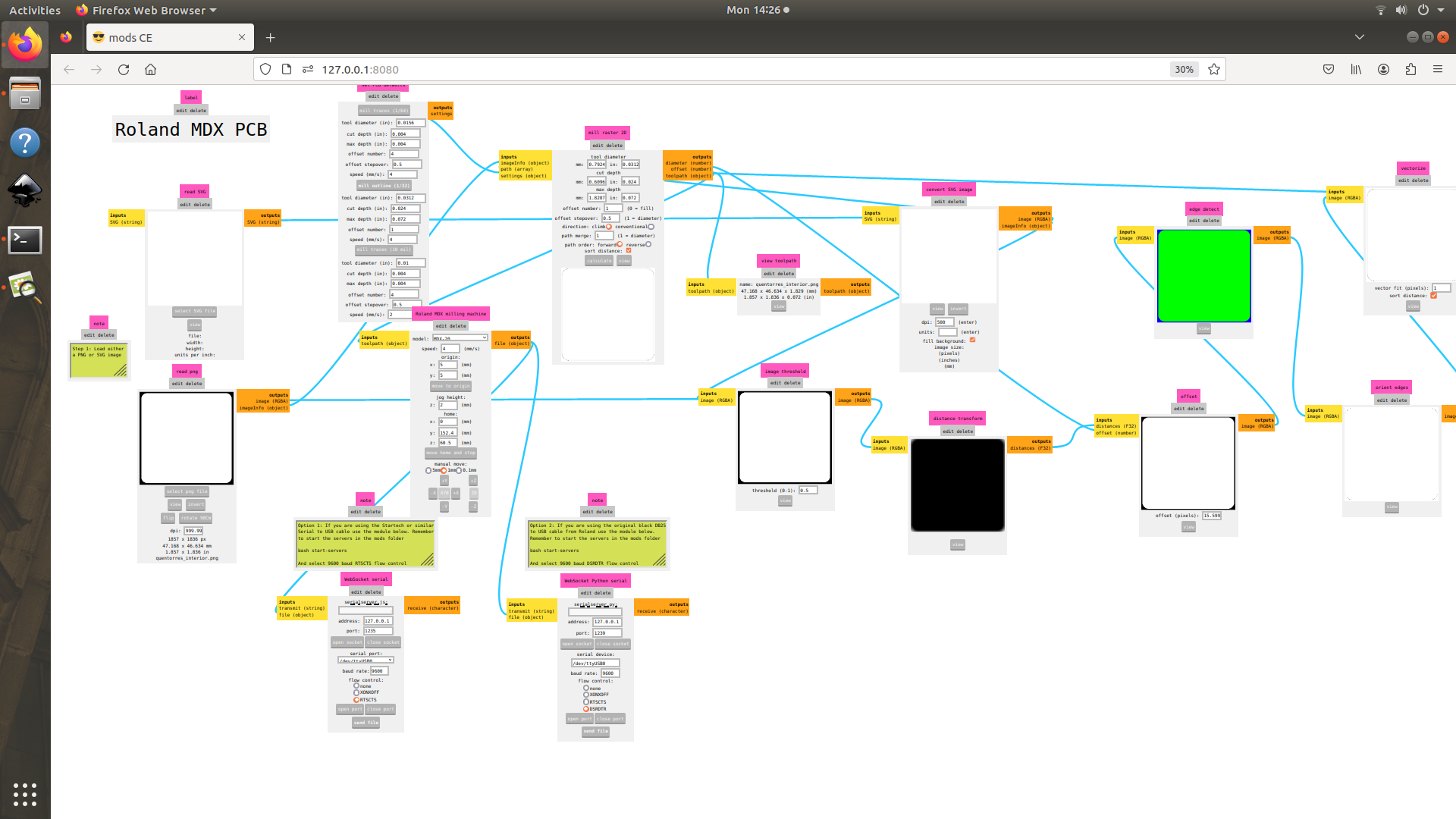
Fab Mods
Mods is a modular digital manufacturing CAM (Computer-Aided Manufacturing) software that is open-source and developed by MIT’s Center for Bits and Atoms (CBA).
This software allows for the unified control of various machines directly from a computer.
It facilitates communication with a range of manufacturing equipment including laser cutters, vinyl cutters, and CNC mills, making it a versatile tool for digital fabrication processes.
The subsequent step involves initiating Fab Mods locally due to issues with the online USB port of the machine.
To commence locally, navigate to the Fab Mods directory in the terminal and execute the "start-servers" file using the following command:
bash start-servers
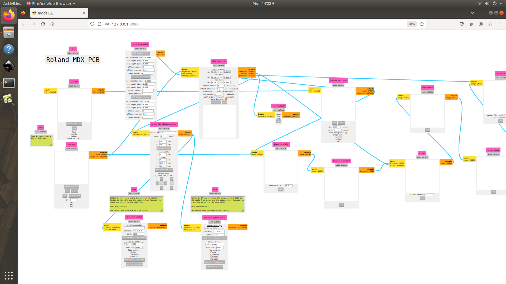
Next, I followed these steps. So, right-click on the screen>programs>open program and this page appears, from this choose PCB under MDX mill
This page appears and here we can choose our files as .png or .svg and then choose our tools.
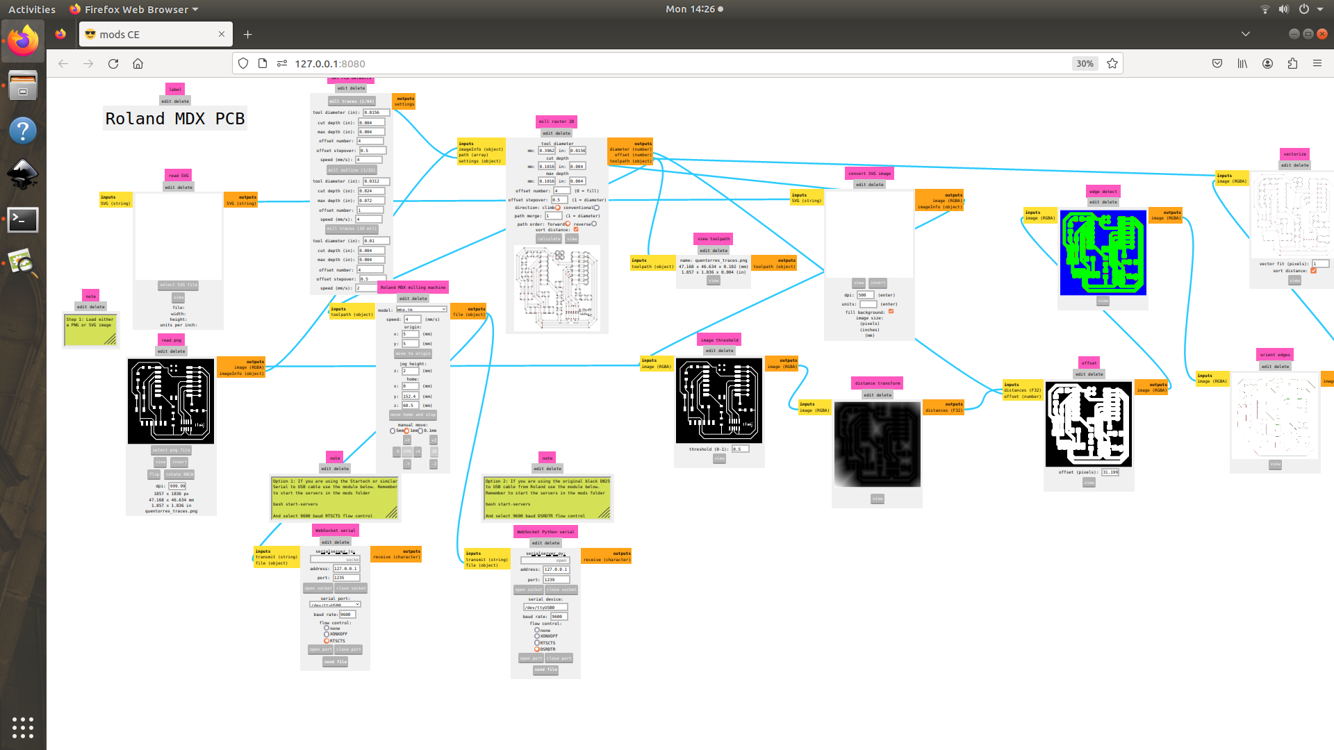
So I uploaded my file as .png and then chose 1/64" as my milling tool and selected calculate.
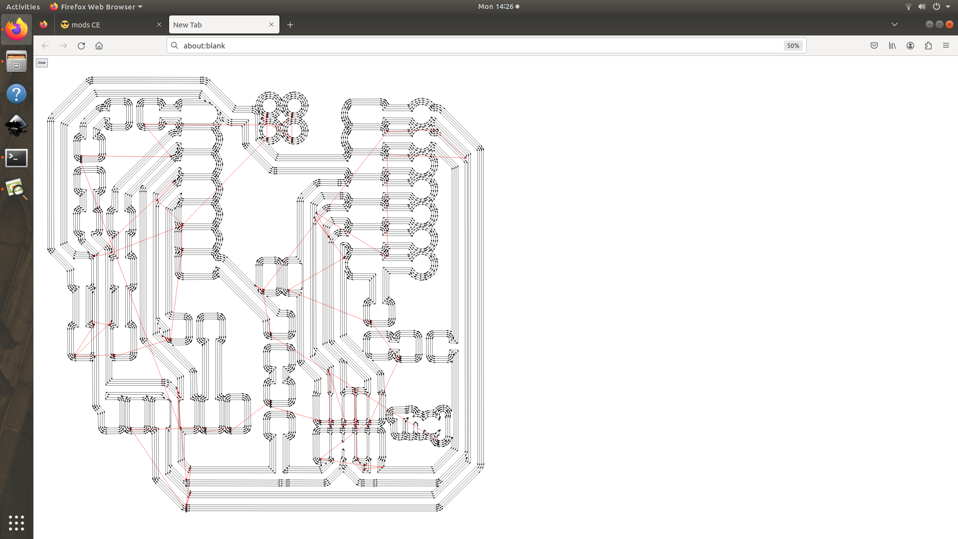
This is the view after calculating. I found out the 'e' in my name wouldn't be milled properly. But I send this file to the machine.
This is the file I sent for drilling, tool was also changed to 1/32".
This is the file I sent for cutting, tool used was 1/32".
Production Process
During the group assignment we were familiarised on how to use the machine for milling. So I followed the same steps to mill my very own pcb.
So first step is to clean the bed of the machine.
I used a steel ruler to take out any residue of glue from previous pcb milled on the machine.
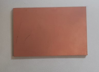
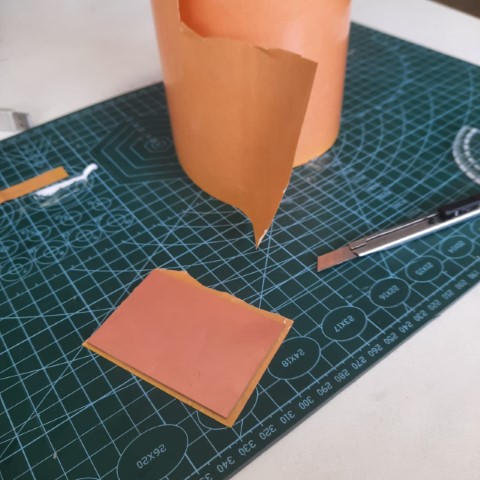
Next, I took my FR1 board from the inventory and stuck the double-sided tape on it to place it on the bed.
There are three steps in the production process- Milling, Drilling and Cutting.
So for milling we use 0.4mm bit and for drilling and cutting, we use 0.8mm bit respectively.
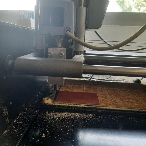
Since, milling was first, I placed the 0.4mm bit in the collet and screwed it tightly. Then, I set the origin using fab mods, x=5 and y=5.
Here is the milling process:
After the milling process, I realised that the right corners hadn't milled properly so I had to mill it again.
Here's the second try:
After the second milling, it had all milled properly and now was the time to drill the holes.
So I changed the bits carefully to 0.8mm and using fab mods set the origin again to x=5 and y=5.
This was a fast process so I wasn't able to record it.
After drilling, I used fab mods to to take the cutting file and uploded it to the machine to start cutting.
Here's the cutting process:
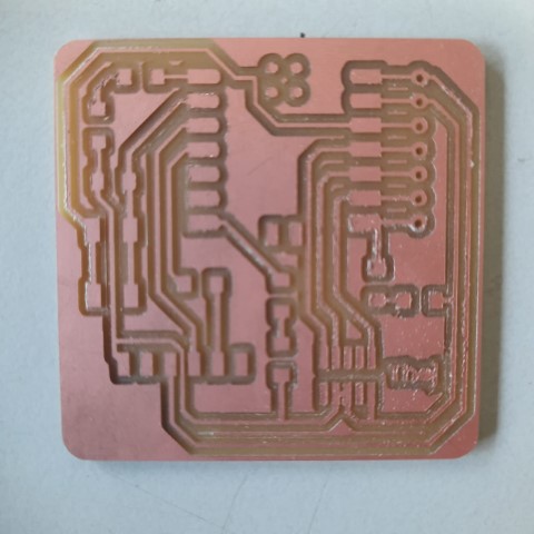
So here's the final result after the all of the production processes
So I used sand paper to give a smooth finish. Now my pcb was ready for the soldering process.
Soldering
Soldering is a process used to join together two or more metal components by melting and flowing a filler metal (solder) into the joint.
The filler metal, typically in the form of a wire or alloy, has a lower melting point than the materials being joined, allowing it to form a bond without melting the base metals.
Soldering is commonly used in electronics, plumbing, metalwork, and jewelry making, among other fields, to create strong and permanent connections between components.
It requires the use of a soldering iron or soldering gun to heat the joint to the appropriate temperature for melting the solder.
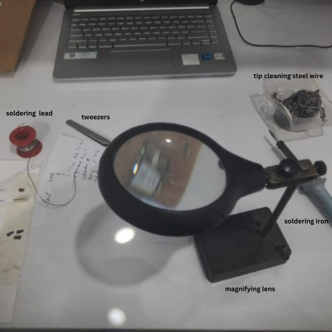
Safety precautions for soldering:
Ensure adequate ventilation in the workspace to prevent inhaling fumes emitted by solder and flux, as they can be harmful.
Utilize fume extractors (fans) or work near an open window to facilitate ventilation.
If you're working in a poorly ventilated area, wear a mask to protect yourself from inhaling harmful fumes.
Utilize tools such as tweezers or clamps to secure components in place, keeping your fingers away from the heat of the soldering iron.
Always return the soldering iron to its stand when not in use, and never leave it unattended while it's still hot to prevent accidents.
After soldering, wash your hands thoroughly to remove any residue and prevent accidental ingestion of harmful substances.
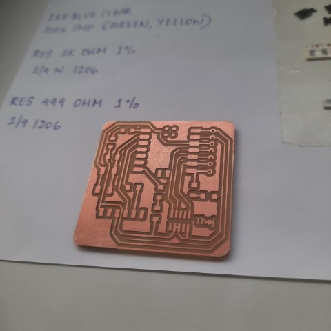
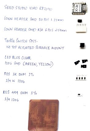
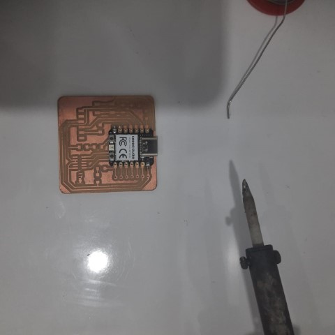
Since my pcb was ready next step is to gather all the components for soldering.
So I requested for components on my FabLab Inventory Website and acquired them.
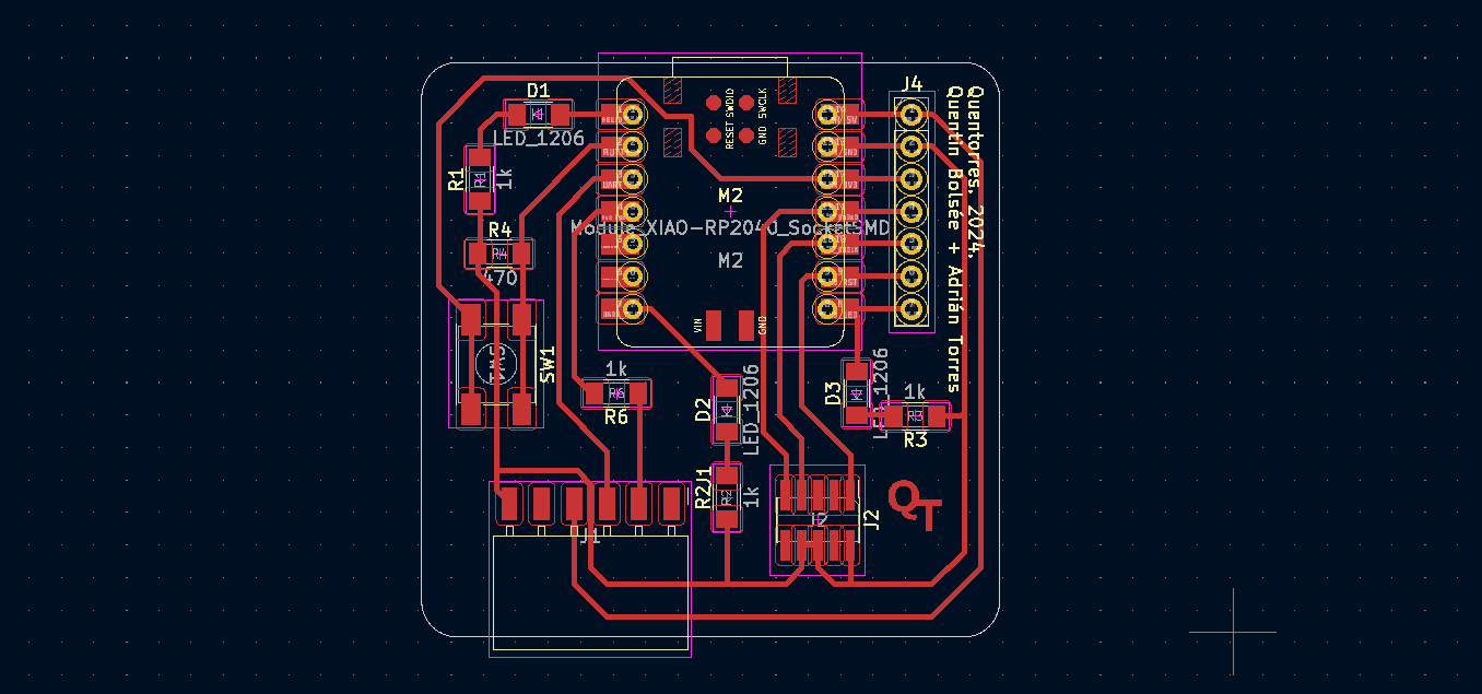
I followed this diagram to solder the components
These are the soldering components available in my lab.
Since it was the weekend, I thought of soldering in my home.
So I set up my table at home for the soldering process.
So I started off by soldering the microcontroller onto the pcb at two corners so that its position would be fixed for easy soldering.
Here is a snippet of me soldering the components. (My Dad comes in between to check up on me).
Here's the board after 95% of soldering process (LEDs are left).
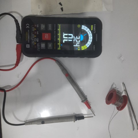
To make sure I don't mix up the polarities of the LEDs I used multimeter to check them one by one.
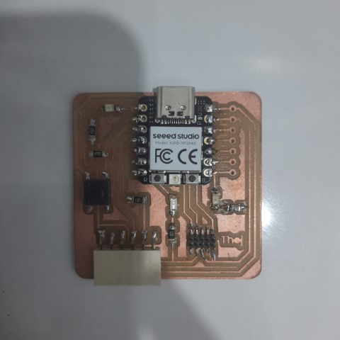
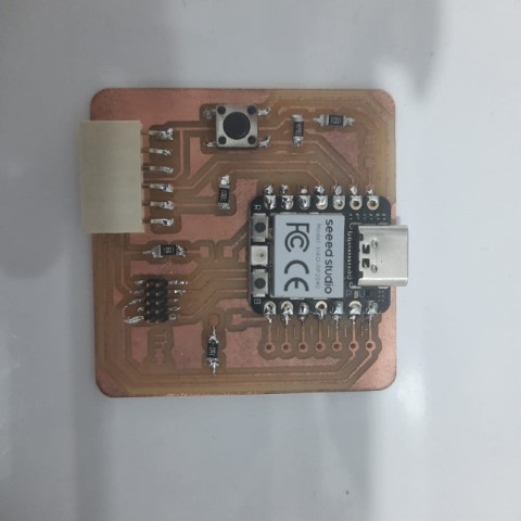
So here's the final result after the full soldering process.
Programming & Testing
So now we have to program and test the board to make sure it works properly.
I followed the steps as mentioned in the website. I had arduino IDE previously installed so I just had to install the board.
File>Preferences>Board Manager and copy paste the link of arduino-pico package.
Then, I installed Raspberry Pi Pico/RP2040 library. It took 5 to 8 minutes for complete installation.
After the installation, I chose the board from Tools>Boards>Raspberry Pi Pico/RP2040>Seeed XIAO RP2040.
Next, I took the Blink program to test the board. It worked perfectly fine with no errors or warnings.
Next, I programmed the board to test the LED at GPIO 26
Here is a snippet of LED blinking at GPIO 26.
Here is a snippet of all LEDs blinking at GPIO 26, 1 and 0.
Here is a snippet of all LEDs chasing at GPIO 26, 1 and 0.
    // Pin connected to the LED
        const int ledPin1 = 26;
        const int ledPin2 = 0;
        const int ledPin3 = 1;

        void setup() {
            // Initialize the LED pin as an output
                pinMode(ledPin1, OUTPUT);
                pinMode(ledPin2, OUTPUT);
                pinMode(ledPin3, OUTPUT);
                }

        void loop() {
            // Turn on the LED
                digitalWrite(ledPin1, HIGH);
                delay(100);
                digitalWrite(ledPin2, HIGH);
                delay(100);
                digitalWrite(ledPin3, HIGH);
                delay(100);  // Wait for .1 second

            // Turn off the LED
                digitalWrite(ledPin1, LOW);
                delay(100);
                digitalWrite(ledPin2, LOW);
                delay(100);
                digitalWrite(ledPin3, LOW);
                delay(100);  // Wait for .1 second
            }
Extras
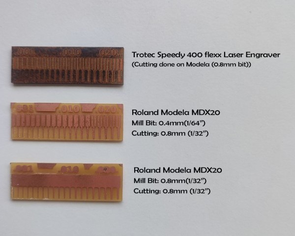
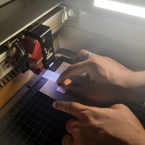
Laser Engraving
Utilized Trotec Speedy400 for precise PCB engraving, Despite eight passes with the Trotec Speedy400, some traces on the PCB weren't fully achieved, potentially affecting the board's functionality.
Further optimization of settings or additional passes may be necessary to ensure complete engraving and proper circuit conductivity for optimal performance.
1. So first set up the cardboard to put the PCB for engraving.
2. Crease the cardboard in the correct shape of the PCB to get its origin for engraving.
3. Start the laser engraving process. However as I mentioned before, some traces werent obtained properly.
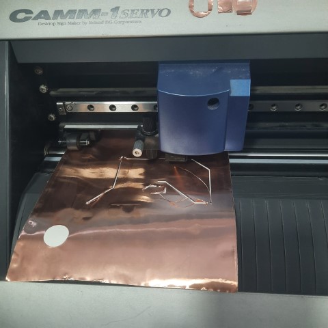
Vinyl PCB
Vinyl cutter was familiarised during week three and therefore used a simple PCB design to cut in copper sheet.
However it was unsucessful, the force and pen force settings were adjusted but a proper pcb wasnt obtained.
A simple PCB design was made in shape of a flower like this.
I exported it was svg file and opened it in Inkscape software to edit it.
Here's how I edited it into. But I wasn't able to get the pcb properly.
So I tried for a smaller version like this. However that didn't workout as well as you can see in the video.
Reflow
Reflow soldering is a technique used to attach electronic components to a PCB.
The process involves heating the solder paste, causing it to melt and form a bond between the components and the board.
This method ensures reliable connections and is commonly used in PCB assembly for its efficiency and precision.
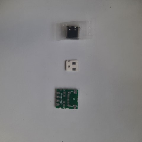
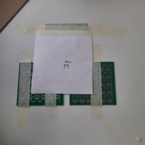
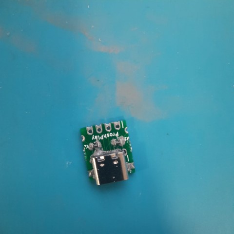
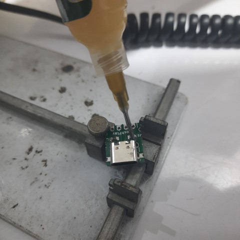
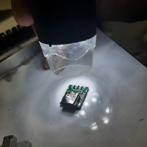
Using this process, I will be soldering these components into the PCB. This PCB was designed by our instructor Saheen and it is a C-type breakout board.
This is our laser cut stencil to apply the solder paste.
So I placed the components after applying the solder paste, and you can see it here.
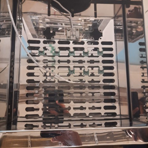
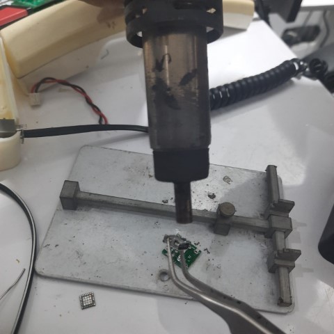
Now I placed it in our reflow oven with my fellow fab mates.
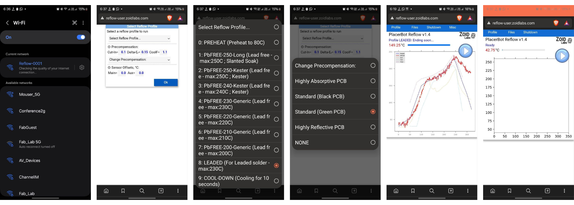
We can connect the oven to our phones using wifi and can monitor the temperature.
They have a mobile interface that can be accessed by connecting to the device using WiFi, allowing users to monitor temperature changes during different phases:
a. Soak Phase: During this phase, the temperature is further increased to ensure the entire assembly reaches a uniform temperature. This helps prevent thermal shock to components and ensures the solder melts evenly.
b. Reflow Phase: In this phase, the temperature is raised above the melting point of the solder, typically ranging from 183°C to 250°C (361°F to 482°F) for lead-free solder. This causes the solder paste to melt, flow, and form solder joints.
c. Cooling Phase: Following the reflow phase, the assembly is cooled in a controlled manner to solidify the solder, forming strong and reliable electrical and mechanical connections.
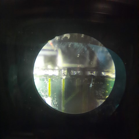
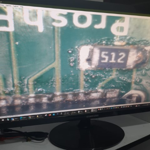
Next, I viewed my PCB through the microscope to identify the short connections. Turns out they were short.
Since it was already night time, I headed home and thought of correcting the short connections.
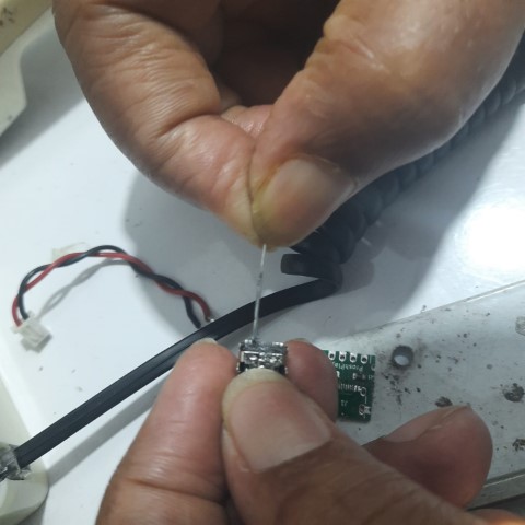
I had no experience with solder pasted components so my Dad helped me out.
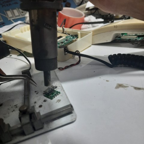
So first, apply some flux onto the faulty connections.
Next by using hot air gun, apply hot air at the point for some time and remove the component.
I used the soldering iron to remove the existing lead on the component and then using a thin stump my Dad applied solder paste.
I didn't do it because there was no stencil.
Now using the hot air gun again, slowly heat the component for the lead to melt and join again.
There was no oven so I had to careful so as to not overheat it.
I checked with the microscope to look for short connections and thankfully none were found.
.png)
.png)

.png)
.png)
.png)
.png)
.png)
.png)

.png)
.png)
.png)
