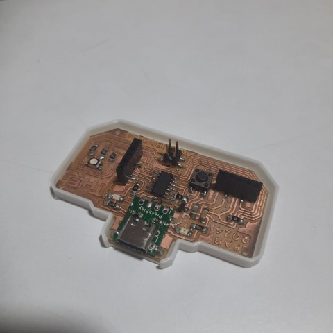
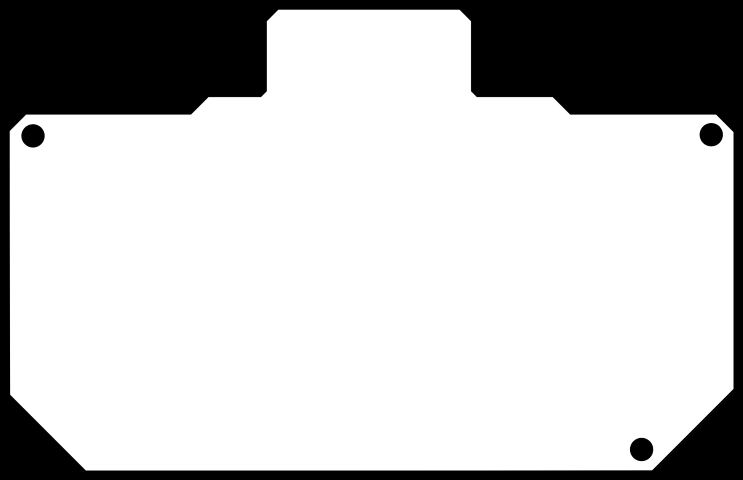
Case
First, I exported the STEP file of the design.
.png)
I created a case offsetting the pcb board
.png)
Here's the output
My plan for this week is to design, mill, test a development board and from that understanding I plan to design the board for my final project.
I'll be designing a development board using SAMD11.
KiCad is an open-source EDA software suite for designing PCBs and schematics. The typical workflow in KiCad involves two primary tasks: drawing a schematic and laying out a circuit board. A KiCad project encompasses various files within a folder, including a project file, schematic, board layout, and potentially other associated files like symbol and footprint libraries, simulation data, and purchasing information.
The process begins with creating a schematic, where components are selected from libraries and connected using wires to represent electrical connections. After completing the schematic, an Electrical Rules Check (ERC) is performed to ensure the design's integrity. It's common for schematics to undergo revisions even after the board layout has begun, necessitating updates and iterations to maintain consistency.
Once the schematic is finalized and passes the ERC, the design is transferred to the board editor. Here, the netlist generated from the schematic is imported, and footprints for components are automatically placed on the board. Designers then arrange these components, taking into account factors like size, placement, and signal routing. Traces are drawn to establish electrical connections between components, adhering to design rules and constraints.
After laying out the board, a Design Rules Check (DRC) is performed to ensure compliance with manufacturing specifications. Any errors or warnings identified during this check are addressed to ensure manufacturability. The board layout undergoes thorough review to confirm alignment with design requirements before saving the final layout.
Once the board layout is complete and passes the DRC, fabrication outputs are generated.
.png)
To add components while designing there are a lot of libraries but for Fab Academy, there is a seperate library with all components. This avoids confusion since there are multiple libraries with same components.
.png)
Next step to follow these installation steps mentioned in the repository for correct access to the library while designing. So i followed those steps.
.png)
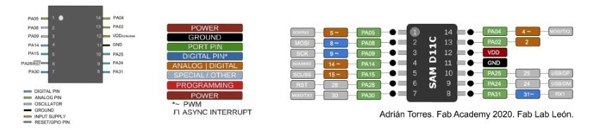
SAM D11 is a microcontroller developed by Microchip Technology. It belongs to the SAM D family of ARM Cortex-M0+ based microcontrollers. SAM D11 microcontrollers are known for their low power consumption, making them suitable for applications where energy efficiency is critical. They are commonly used in various embedded systems, IoT devices, consumer electronics, and other applications requiring low-power operation and moderate processing capabilities. SAM D11 microcontrollers typically feature a range of peripherals such as ADCs, UARTs, SPI, I2C, timers, and GPIOs, making them versatile for a wide array of applications.
For my development board, I'm using this microcontroller SAMD11. So I used this pin out diagram to understand the microcontroller and use it in my design accordingly.
SAMD11 runs on 3.3V but the laptop output voltage is 5 V. To regulate the voltage, I referred this design so my board would not damaged.
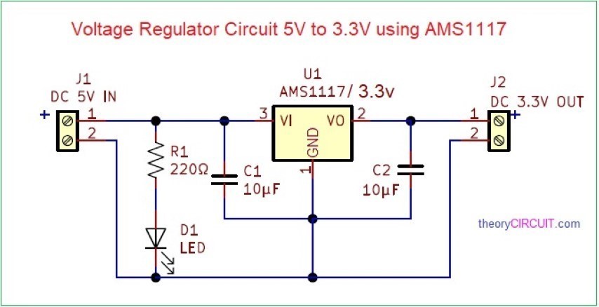
Here is the regulator circuit
.png)
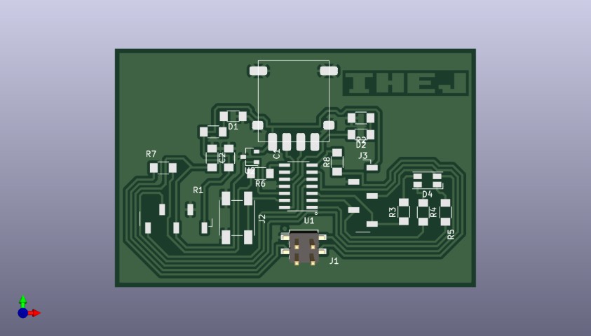
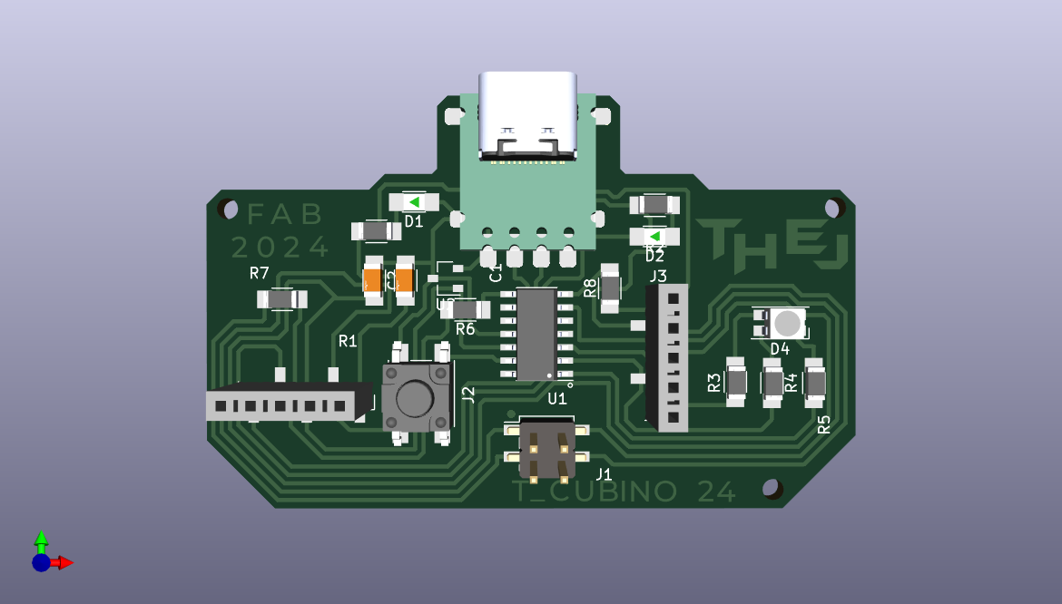
Here is the design with all components:
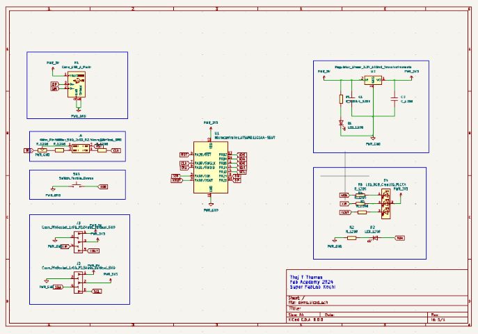
To understand the design, so I have made a voltage regulator circuit so as to get 3.3V for the microcontroller. I am using 1x04 header pin instead of 2x05 header pins for easy soldering. USB_A plain is actually a dummy for USB C type breakout board we had soldered in the week of electronics production. I have added an LED and a button, also 2 pin sockets. One socket is for I2C, I have taken SDA and SCL from the chip to the socket along with 5V, 3.3V and GND. Next socket, I took XIN, XOUT, remaining digital pin, GND and 5V onto the socket. I have labeled all the pins to the board.
.png)
.png)
.png)
.png)
.png)
.png)
.png)
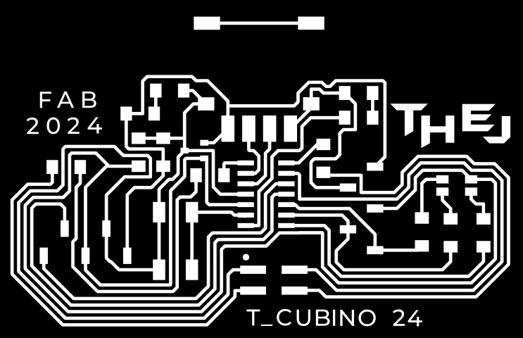
Next step is to export the Gerber file and convert it into PNG for milling. Our FabLab has a special website for this conversion. Visit this website.
.png)
.png)
.png)
.png)
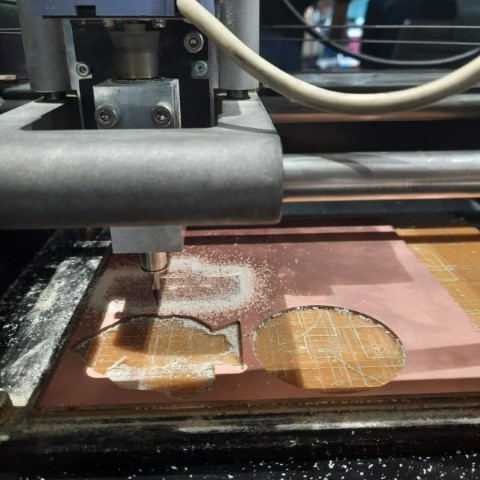
Next step is the production of the design.
During week four of electronics production, I was introduced to PCB milling of Quentorres Board by Roland Modela MDX20. Therefore, I'll be implementing the same workflow.
Here's a snap during the milling process
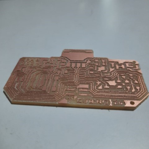
PCB is ready, it needs sanding.
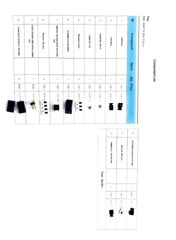
Resistor and capacitor values were found out based on datasheet and rounded off to its availability in the lab.
From the schematic and referring the datasheet, I used this site to calculate values,
however it was rounded off to the availability.
R1= 499 Ω
R2=R3=R4=R5= 100 Ω
C1= 1 uF
C2= 100 nF
So I requested for all components on FabLab Inventory Website and acquired them.
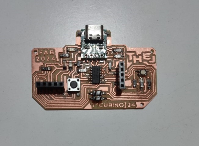
Now with the components acquired, next step is to solder them onto the PCB. So I got my workstation just like I did in week four and started the process.
The microcontroller and the regulator IC was difficult to solder owing to the small size. But somehow I managed to solder it without using a lens. 1206 SMDs were easier and rest all pin headers, sockets and button was easy due to its large size. We had a C-type breakout board which was designed by one of our instructor and soldered using reflow during week four. So I soldered that as well. Here's the result:
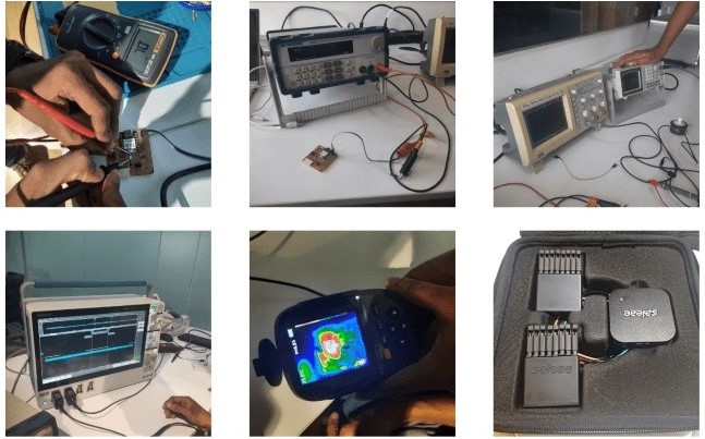
Next step is to program and test the board so I followed the this documentation on how to use the Quentorres board as a programmer.
I got the ribbon cables ready and the SWD converter.
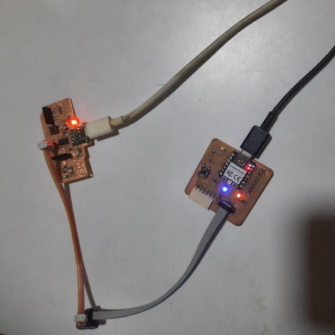
I followed the same steps as the documentation.
.png)
.png)
.png)
.png)
.png)
While debugging, it was found that my ribbon cable wasn't functioning properly
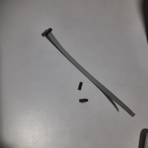
Sucessful with another ribbon cable
.png)
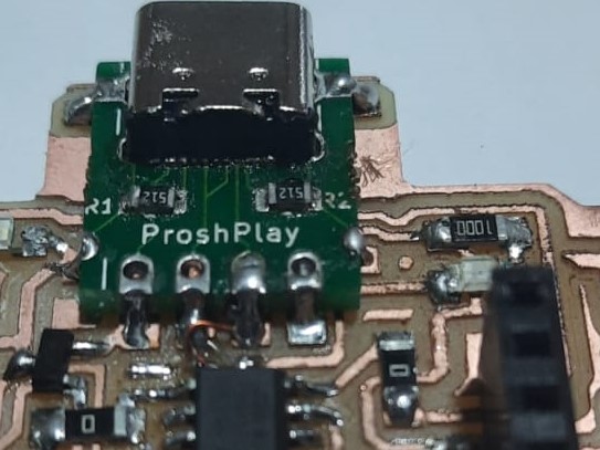
Port wasn't getting detected in the arduino IDE. While debugging it was found that while soldering one of my connection was short. So corrected that connection and tried again. But the error still persisted. Then it was found that DP and DM had interchanged in the PCB design even though the schematic was correct. There was some issue with the library of our C-type connector. Since the milling was already done, the solution was to cut the connection and add jumper wire.
All errors were rectified and the port was getting detected.
.png)
As we had programming in week six, I did the same workflow this time as well.
    const int buttonPin = 2; // Button pin from SAMD11C14A
    const int ledPin = 4; // LED pin from SAMD11C14A
    int ledState = LOW; // Current LED state
    bool previousButtonState = HIGH; // Previous button state, assuming pull-up

    void setup() {
    pinMode(ledPin, OUTPUT); // Initialize LED pin as output
    pinMode(buttonPin, INPUT_PULLUP); // Initialize button pin as input with pull-up resistor
    }

    void loop() {
    bool currentButtonState = digitalRead(buttonPin);
    if (currentButtonState == LOW && previousButtonState == HIGH) {
        // Button was pressed
        ledState = !ledState; // Toggle the LED state
        digitalWrite(ledPin, ledState); // Set the LED to the new state
    }
    previousButtonState = currentButtonState; // Update the previous button state
    }
The code uploaded sucessfully!
.png)
    const int redPin = 5;    // Red pin of the RGB LED
    const int greenPin = 8;  // Green pin of the RGB LED
    const int bluePin = 9;   // Blue pin of the RGB LED

    void setup() {
        pinMode(redPin, OUTPUT);    // Initialize Red pin of the RGB LED as output
        pinMode(greenPin, OUTPUT);  // Initialize Green pin of the RGB LED as output
        pinMode(bluePin, OUTPUT);   // Initialize Blue pin of the RGB LED as output
    }

    void loop() {
        // Turn on red
        digitalWrite(redPin, LOW);
        digitalWrite(greenPin, HIGH);
        digitalWrite(bluePin, HIGH);
        delay(500);

        // Turn on green
        digitalWrite(redPin, HIGH);
        digitalWrite(greenPin, LOW);
        digitalWrite(bluePin, HIGH);
        delay(500);

        // Turn on blue
        digitalWrite(redPin, HIGH);
        digitalWrite(greenPin, HIGH);
        digitalWrite(bluePin, LOW);
        delay(500);

        // Turn on yellow (red + green)
        digitalWrite(redPin, LOW);
        digitalWrite(greenPin, LOW);
        digitalWrite(bluePin, HIGH);
        delay(500);

        // Turn on cyan (green + blue)
        digitalWrite(redPin, HIGH);
        digitalWrite(greenPin, LOW);
        digitalWrite(bluePin, LOW);
        delay(500);

        // Turn on magenta (red + blue)
        digitalWrite(redPin, LOW);
        digitalWrite(greenPin, HIGH);
        digitalWrite(bluePin, LOW);
        delay(500);

        // Turn on white (red + green + blue)
        digitalWrite(redPin, LOW);
        digitalWrite(greenPin, LOW);
        digitalWrite(bluePin, LOW);
        delay(500);
    }
First, I exported the STEP file of the design.
I created a case offsetting the pcb board
Here's the output