WEEK 8
Electronics Design
Group Assignment:
- Use the test equipment in your lab to observe the operation of a microcontroller circuit board
- Send a PCB out to a board house.
Individual Assignment:
- Use an EDA tool to design a development board to interact and communicate with an embedded microcontroller, produce it, and test it.
Schematic Editor
Similar to week 6, also this week we aimed to design a PCB on Kicad. Week 6 was my first time using Kicad for designing a PCB so it was so confusing. However, this week I could follow the instructions better.
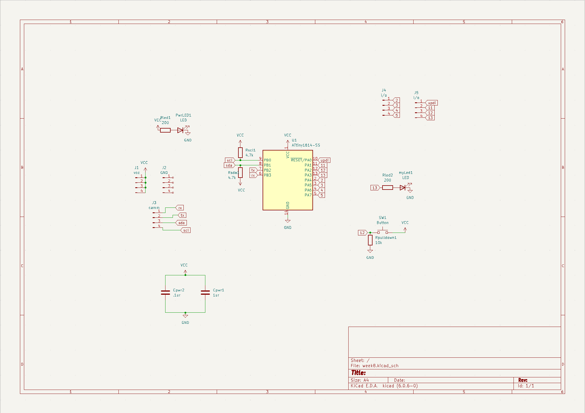
For designing a PCB there are some crucial components to have in the schematic. Such as; pin headers, buttons, LED, ground, and voltage indicators
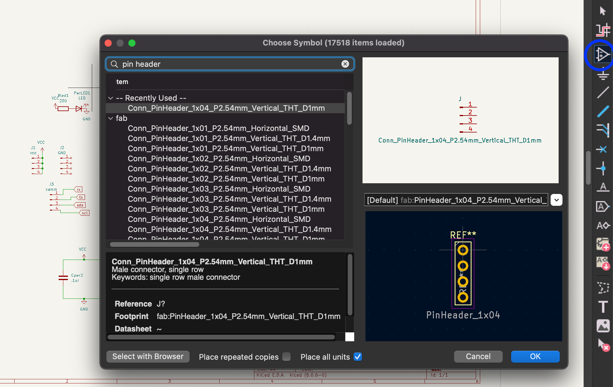
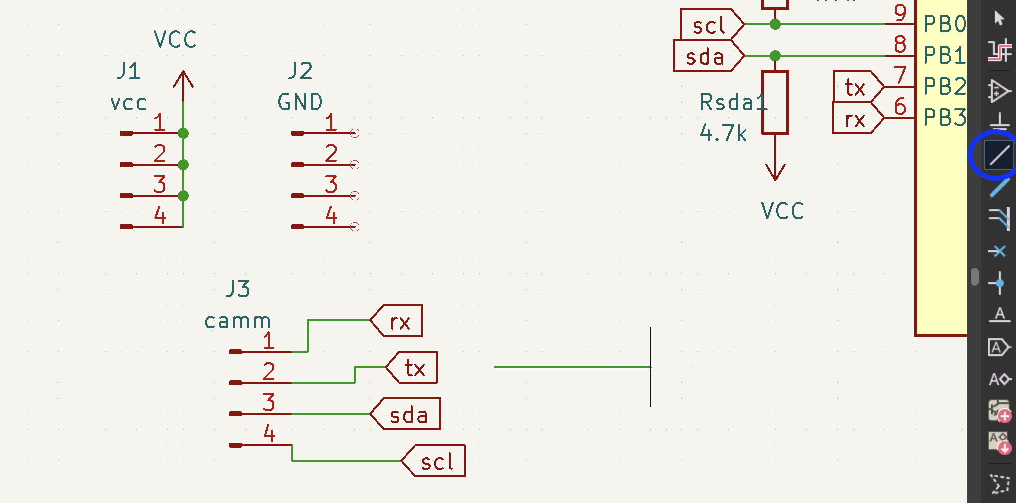
To add these components to the schematic, we used Fab Library in KiCad. After downloading the library to your PC, you can reach components on the right sidebar by clicking the related icon .
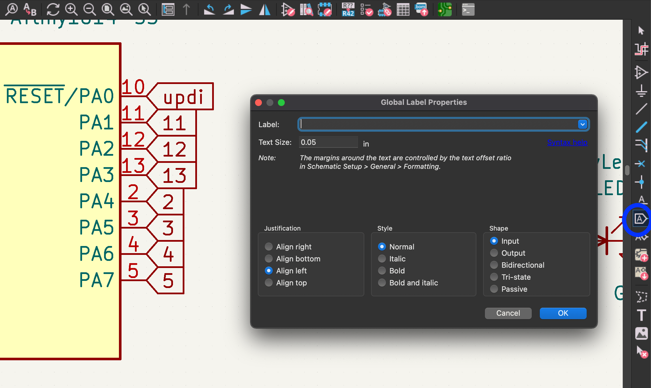
To add a global label, you can click the related icon on the right side bar. When you create a new label, just click where you want to place it.
- To arrange the direction of the component ---> Press R
- To duplicate the component ----> Press D
- To move the component ----> Press M
- To change the name of the component ----> Double click the name and set a new one.
To wire the components to each other, find the stick icon on the right sidebar. Then you have a green wiring tool. When you click one of the components, by moving your mouse you can determine the path of the wire.
Board Editor
When you finish your schematic, open it on the PCB editor by clicking the icon on the top bar.

When you transfer your schematic to the PCB editor, you have an unorganized version of the components. Organizing all components logically is quite important because on the soldering part closeness of the components is essential for having quality soldering.
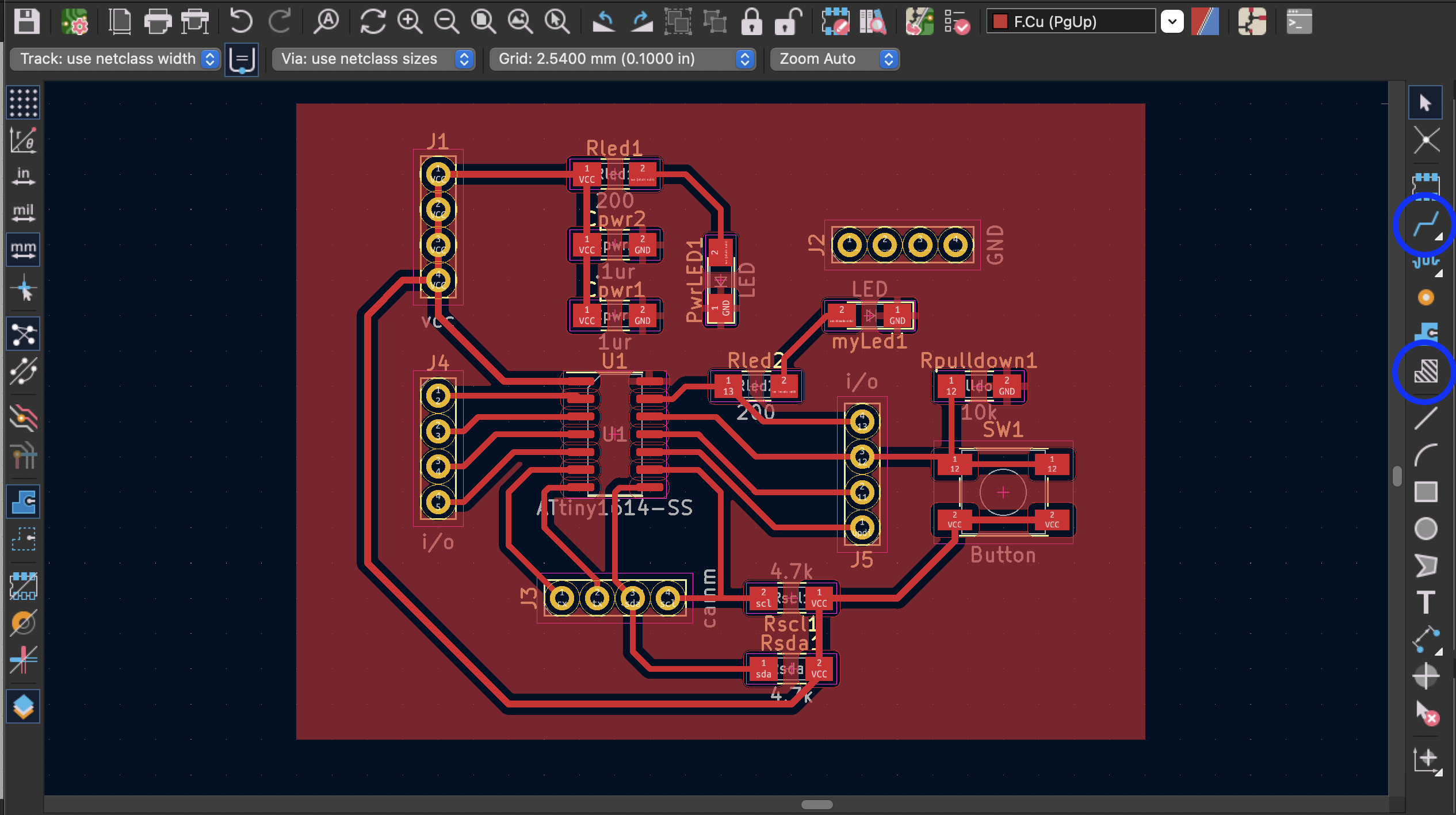
Once you finish the placement, before connecting the components you should set the border of the PCB. Therefore, select the rectangle tool on the right sidebar and determine the border.
When you transfer a component to the editor, it shows you which component must be connected. After finishing the placement of the component, by clicking the wiring tool on the right sidebar, follow the white lines that Kicad shows you to connect the components.
After connecting the components, if you want to change one of the component's placements, a black gap occurs under it. To correct this issue press "B". Then the black area turns into red again.
This week was a repetition of week 6. For the following task of this week, I want to design a PCB for my final project.
PCB Design for Final Project
The starting point of PCB design was to decide what features I wanted to have in my final project design and design my board accordingly. For this reason, I spent a lot of time on my PCB design to determine my needs in my final design and built my board accordingly. Basically, I needed the following on the PCB;
- Microcontroller- XIAO ESP32S3
- Pins for LED
- Pins for Touch sensor
- Extra pins
- Power connection module
To design my PCB I used the Kicad application as I learned during the electronics manufacturing week. To design my PCB, I used the Kicad program as I learned during the electronics production week. In the Schematic Editor interface of the Kicad software, the user can decide which parts will be on the board and how they will be connected to each other. I used the tools on the right side of the screen to make these arrangements.
I used the triangle sign in the third row from the top right to access the symbol library. I found the parts I needed in the Fab academy library. I connected the parts I placed on the screen by clicking the line sign in the 5th row from the top right.
***Although I used XIAO ESP32S3 in my PCB design, I used the XIAO ESP32C3 symbol in Kicad because the XIAO ESP32S3 library is not currently provided and both microcontrollers have the same outputs.
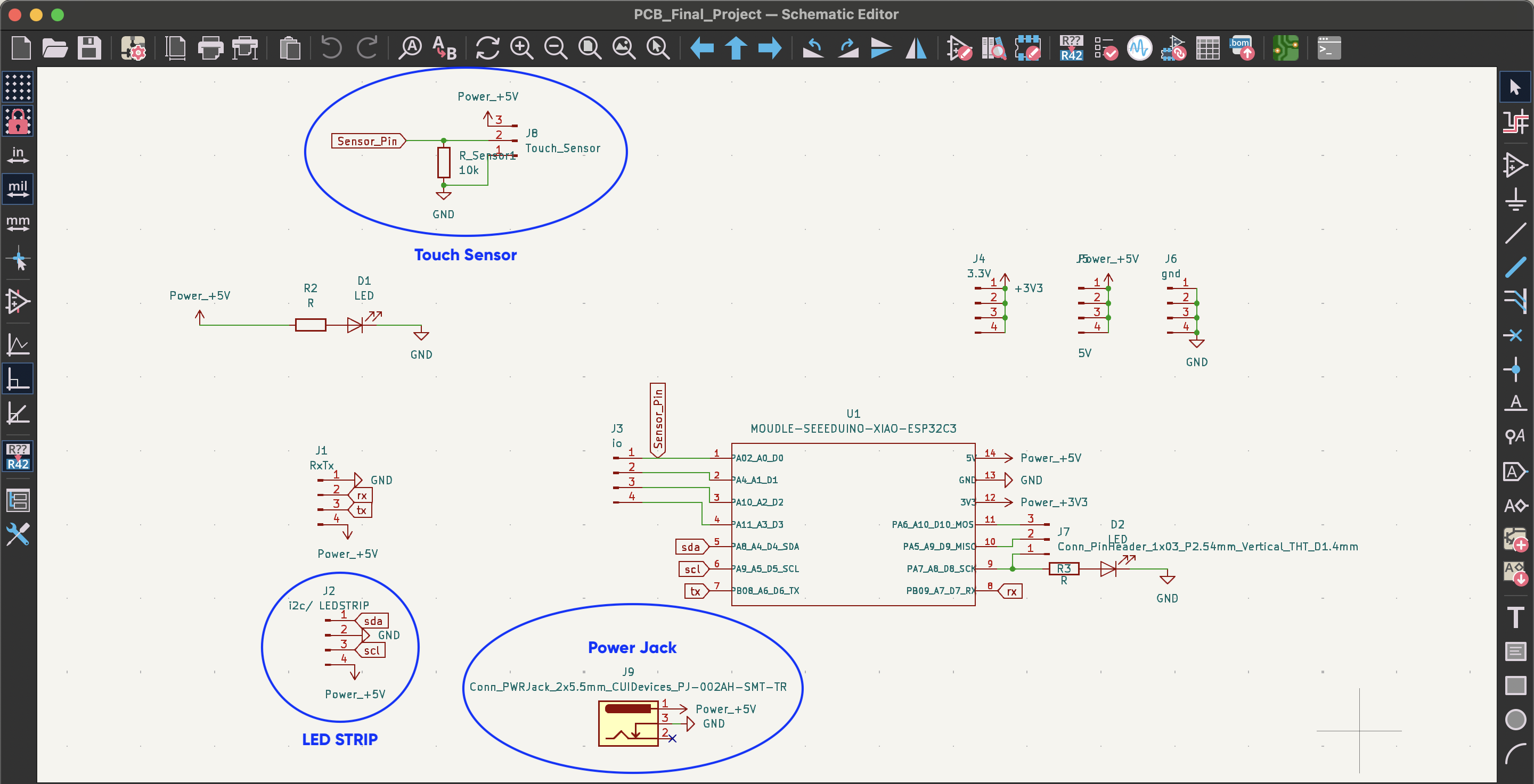
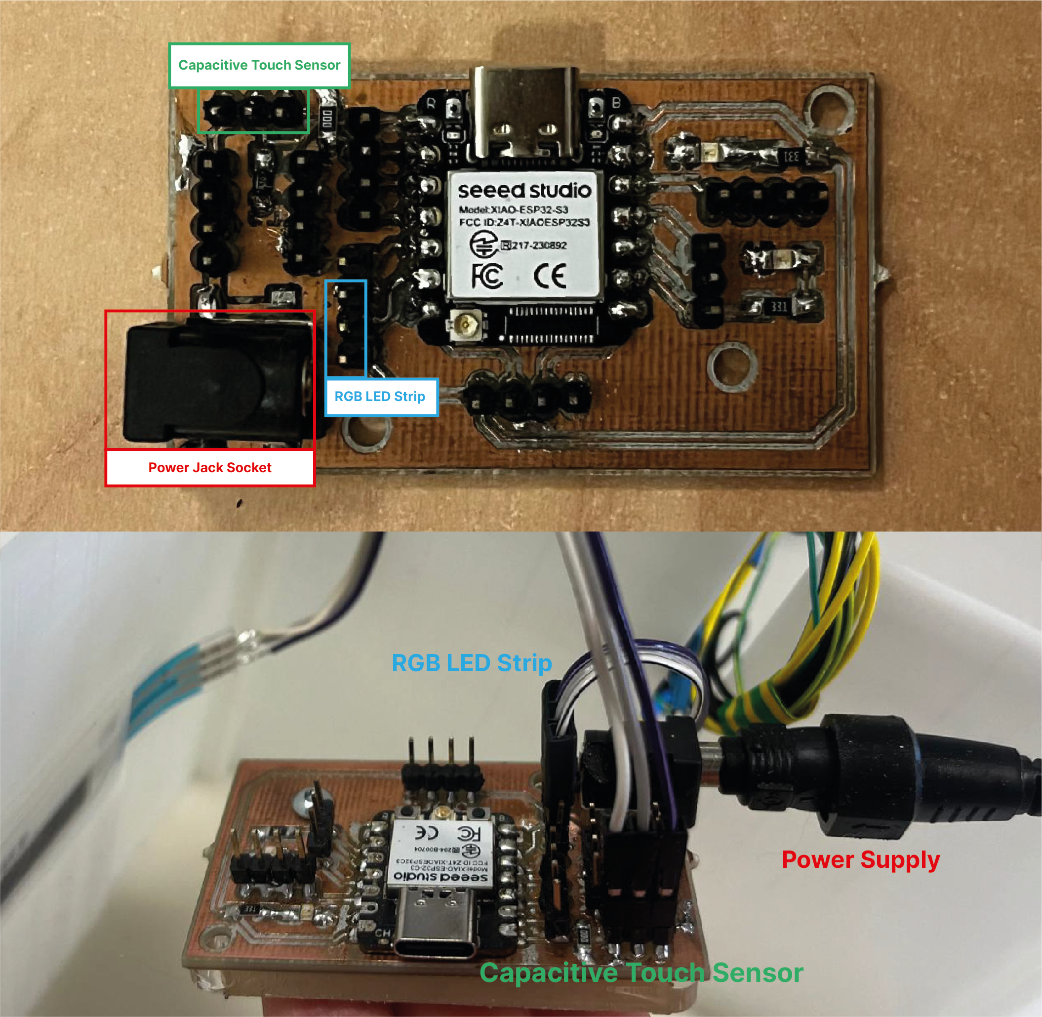
- I connected the touch sensor with 10k resistor, 5V and ground.
- I used a 4-pin header for the ledstrip, I connected ground and 5V to the outputs.
- I connected the power jack with 5V and ground. I did not add anything to one output because when I measured the part I used with an ammeter, I saw that one leg of the part was not connected to anything.
- I also added symbols to the outputs of the microcontroller. These are 3.3V, 5V, ground.
After completing the pin placements and connections, I prepared my design for the PCB editor by following the tools- anotate schematic path. After completing this process, I transferred my drawing to the PCB editor by clicking on the second green box from the right on the top bar.
After transferring my design to the PCB editor, I determined the position and orientation of the parts. For this, following the white arrows made my job much easier. After my placement, I created paths between the parts that need to be connected to each other. By clicking on the cable marker in the right column, third from the top, I got the “Route tracks” tool. After transferring my design to the PCB editor, I determined the position and orientation of the parts. For this, following the white arrows made my job much easier. After my placement, I created paths between the parts that need to be connected to each other. By clicking on the cable marker in the right column, third from the top, I got the “Route tracks” tool.
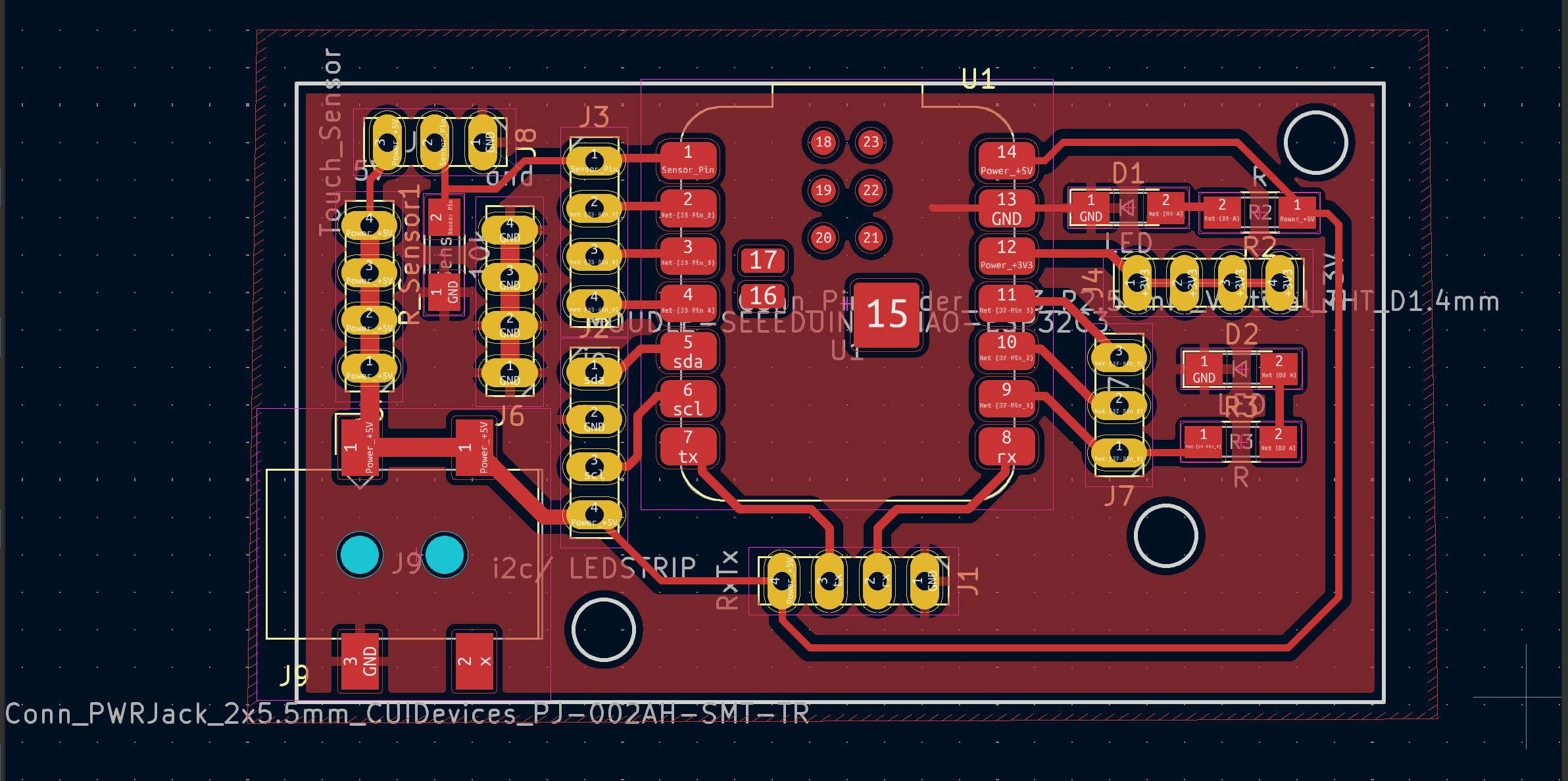
When my design was finished, I prepared my files to create my PCB on the milling machine. For this, I followed this path. File --- Fabrication output --- gerber file. Then, in the window that opens, Plot --- Generate drill file ---- Generate drill file.
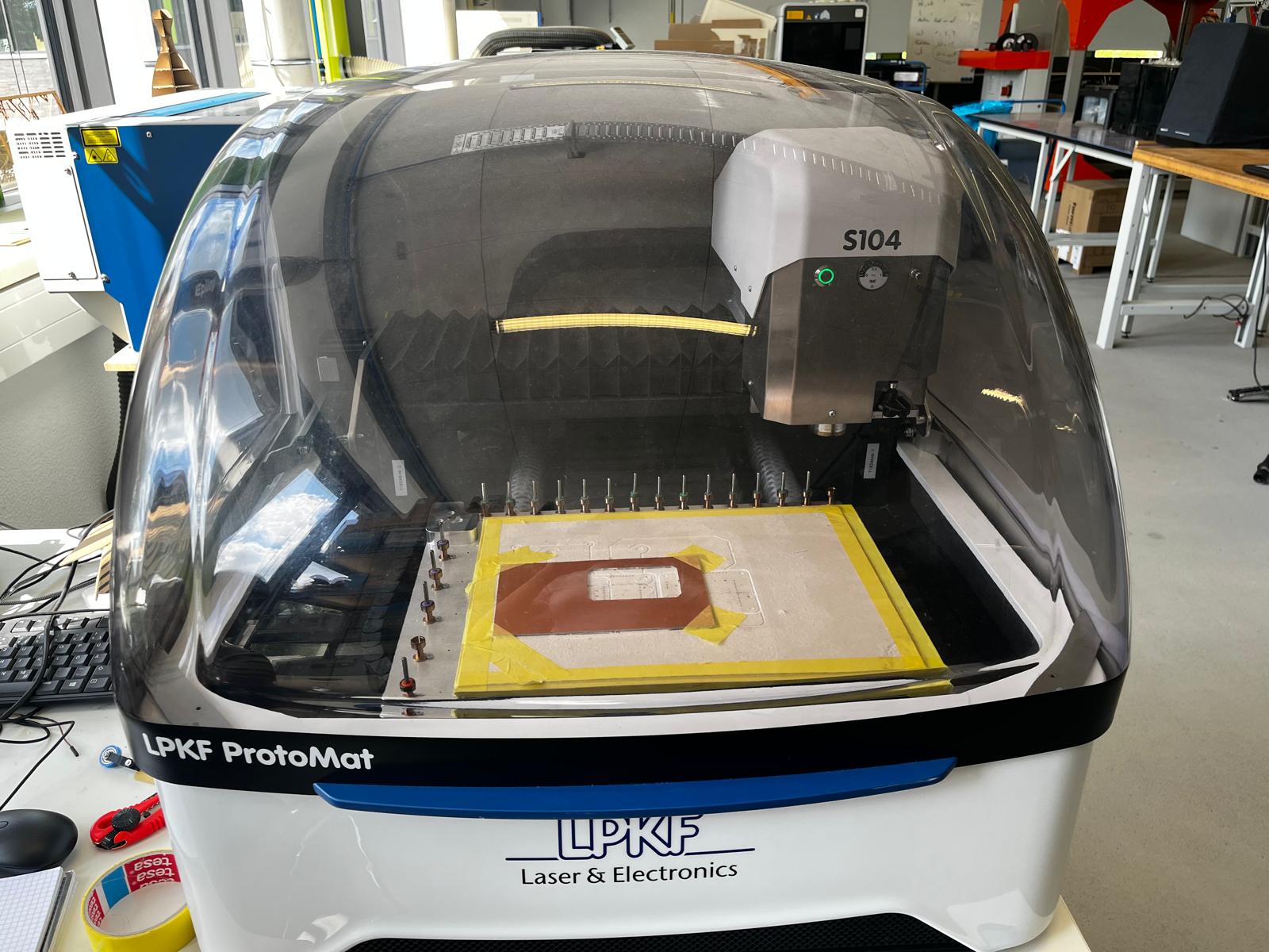
At FabLab Kamplinrfort we use the LPKF laser machine to create our boards. Before transferring my files to the computer, I placed the cutting board on the machine as shown in the image. Using the LPKF machine is a bit confusing and the steps are hard to remember. Although this is the second time I have applied this process, I needed help from my supervisor.
I made the following adjustments on the software respectively;
- Choose templates as - single sided top
- Choose files and import
- Click on the icon that looks like a pinhole at the top left of the screen and open the "technology dialogue" page - copper layer thicknes: 35mm, isolation: 3 chanells.
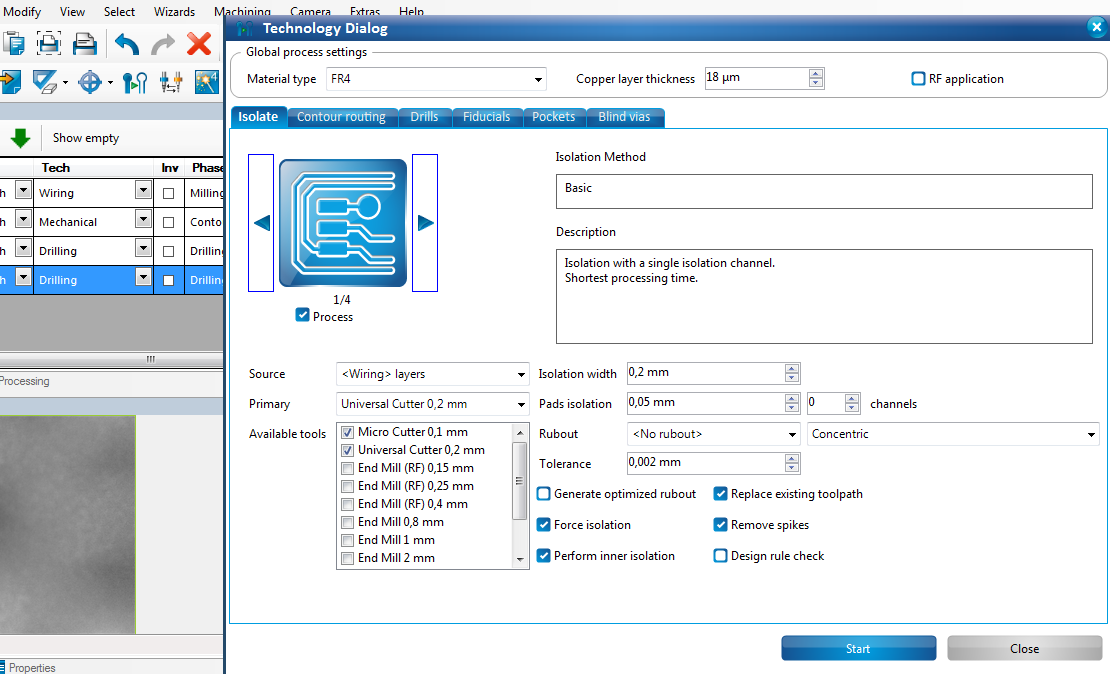
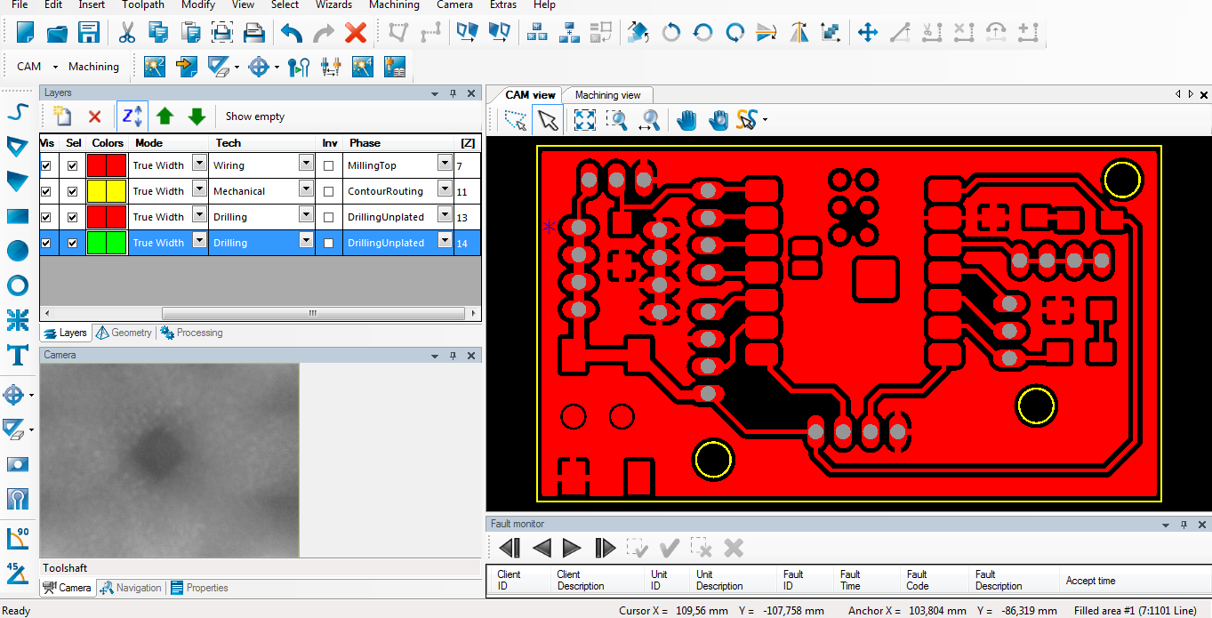
- On the main screen where I uploaded the files, I specified the data about which file will be cut and how. You can see this in the image below.
- To start cutting the board, click on the icon that looks like a magic wand and open the "Board production wizard"
- The machine will want to know where to start cutting, so use the interface to determine where to cob the cutter head and start cutting.
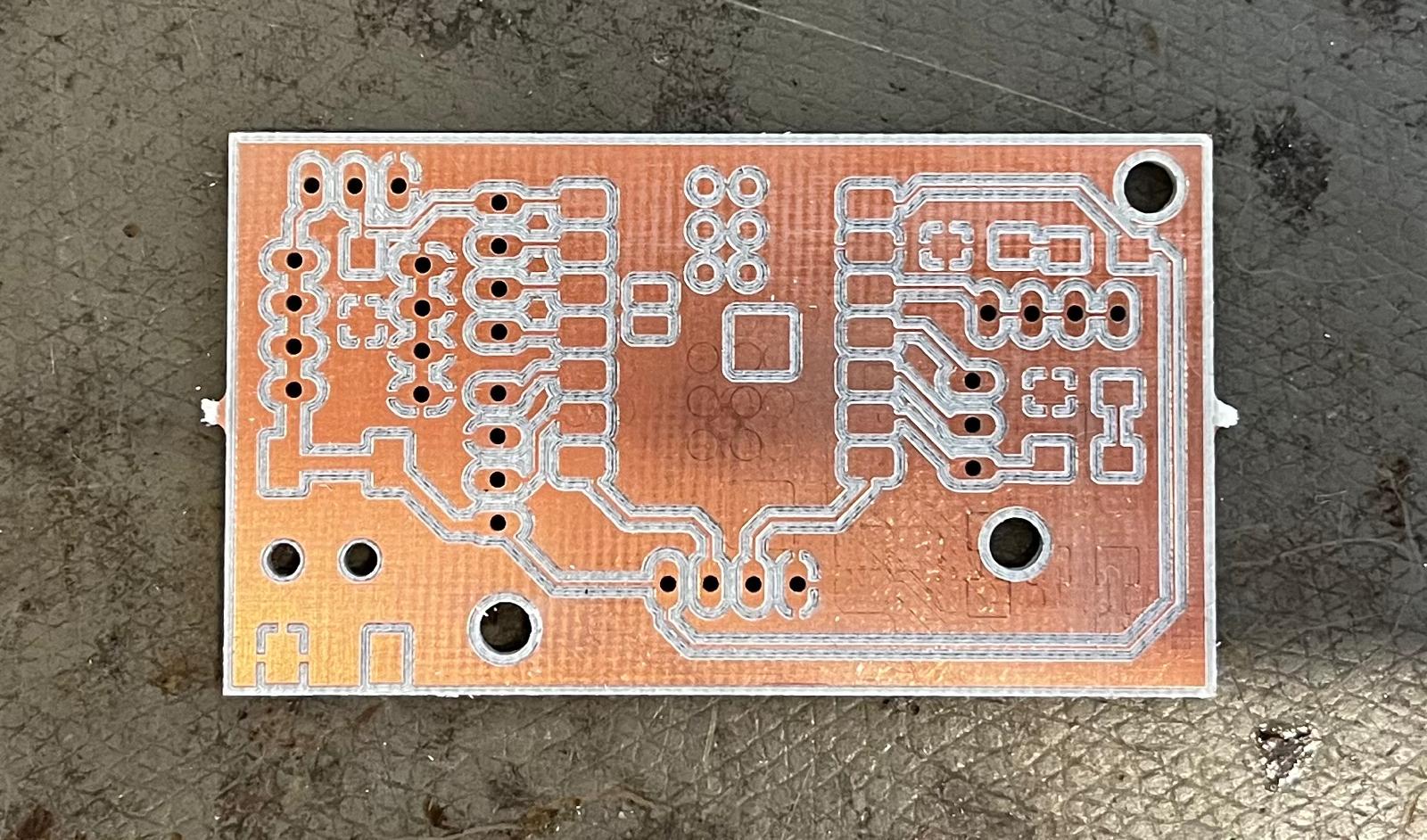
Testing PCB
I would like to explain how the PCB works and how it communicates with the computer through my experiences while testing the sensor I used in my final project. I therefore followed these steps;
- I connected the PCB to my computer via a usb cable.
- I opened the Arduino IDE application and found my PCB by following this path. Tools--- Board --- XIAO ESP32-S3
- I followed this path to find the port that connects to the PCB. Tools--- Port --- USB modern
- In my final project I used a touch sensor and I needed a code sequence to control this sensor. I placed the required code in the software.
- After having the code, I sent the code to the pcb by clicking on the arrow in the upper left corner of the application.
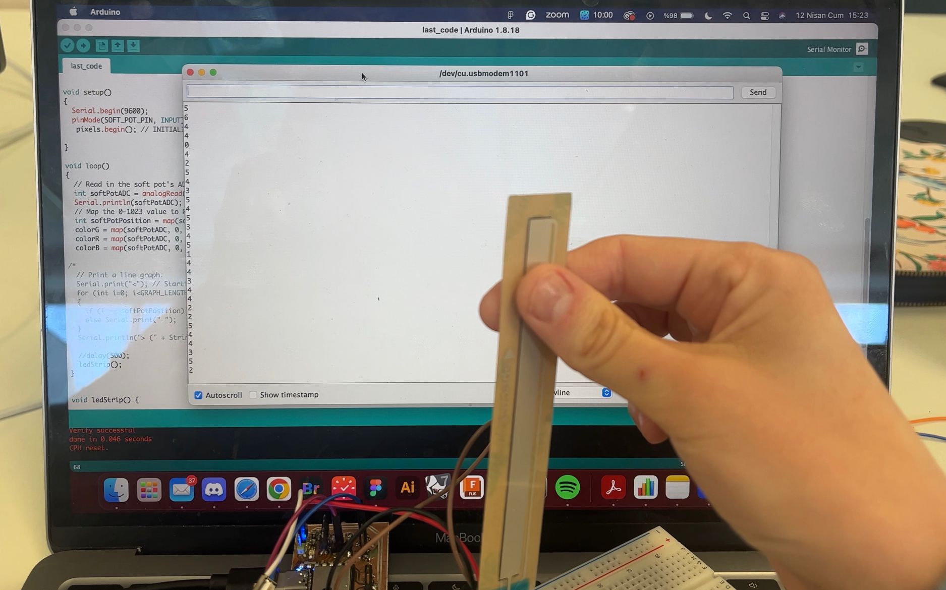
- Now, when I press different parts of the sensor, some data should go to the computer. To check this, I opened the serial monitor tab in the Arduino IDE software.
- I opened the serial monitor screen by clicking on the magnifying glass icon in the upper right corner of the interface. I saw that I got different values when I pressed different parts of the sensor. So the PCB was working.
#include

const int SOFT_POT_PIN = A0; // Pin connected to softpot wiper

const int GRAPH_LENGTH = 8; // Length of line graph


// Which pin on the Arduino is connected to the NeoPixels?
#define PIN        D5 // On Trinket or Gemma, suggest changing this to 1

// How many NeoPixels are attached to the Arduino?
#define NUMPIXELS 180 // Popular NeoPixel ring size


Adafruit_NeoPixel pixels(NUMPIXELS, PIN, NEO_GRB + NEO_KHZ800);

#define DELAYVAL 50 // Time (in milliseconds) to pause between pixels

int brightness =0 ;

int oldBrigthness = 0;

int colorG =0 ;
int colorR =0 ;
int colorB=0 ;

int tempValue = 0;


void setup()
{
Serial.begin(9600);
pinMode(SOFT_POT_PIN, INPUT);
pixels.begin(); // INITIALIZE NeoPixel strip object (REQUIRED)

}

void loop()
{
// Read in the soft pot's ADC value
int softPotADC = analogRead(SOFT_POT_PIN);
//Serial.println(softPotADC);
// Map the 0-1023 value to 0-40
int softPotPosition = map(softPotADC, 0, 4095, 0, GRAPH_LENGTH);
tempValue = map(softPotPosition, 0, GRAPH_LENGTH, 0, 255);
Serial.println(tempValue);

if (tempValue != 0){
brightness=tempValue;
if (tempValue < 33) brightness=0;

if(brightness!=oldBrigthness)ledStrip();

}


/*colorG = map(softPotADC, 0, 1023, 0, 255);
colorR = map(softPotADC, 0, 1023, 0, 255);
colorB = map(softPotADC, 0, 1023, 0, 255);*/

//delay(500);
}

void ledStrip() {
pixels.clear(); // Set all pixel colors to 'off'

// The first NeoPixel in a strand is #0, second is 1, all the way up
// to the count of pixels minus one.
for(int i=0; i< NUMPIXELS; i++) { // For each pixel...

	// pixels.Color() takes RGB values, from 0,0,0 up to 255,255,255
	// Here we're using a moderately bright green color:
	pixels.setPixelColor(i, pixels.Color(brightness, brightness, brightness));

	pixels.show();   // Send the updated pixel colors to the hardware.

}
oldBrigthness=brightness;
}
