WEEK 4
Electronic Production
Group Assignment:
- Characterize the design rules for your in-house PCB production process.
Individual Assignment:
- make and test a microcontroller development board.
1. Schematic Drawing
To draw a schematic, I use the KiCad program. I made a drawing for the SeeeduinoXIAO microcontroller in KiCad. In the KiCad interface, I selected the buttons, LEDs and pins to be connected to the microcontroller and created paths for their connection to the SeeeduinoXIAO. Apart from this, I determined the way the microcontroller receives power and which way it is connected to the ground.
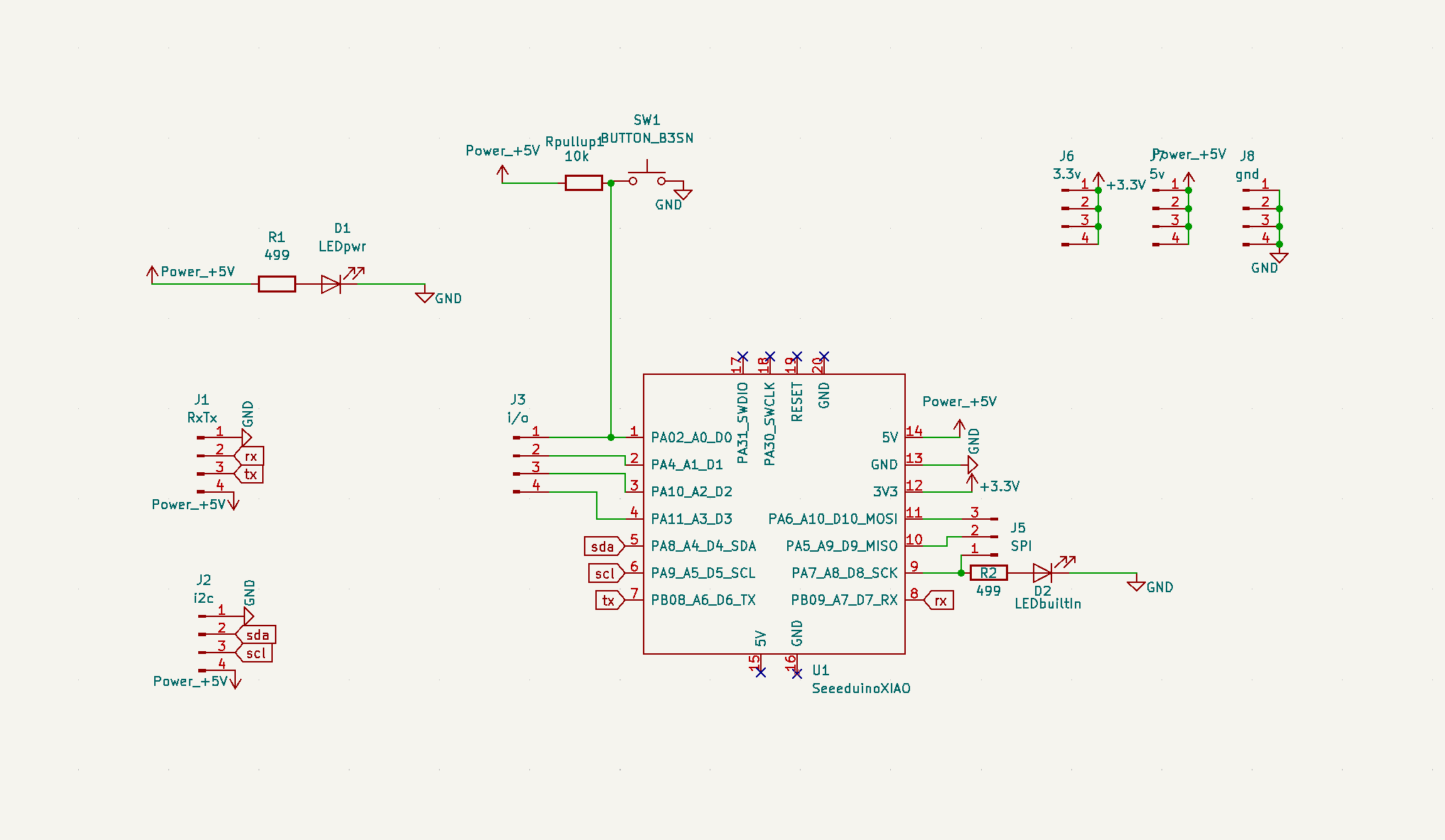
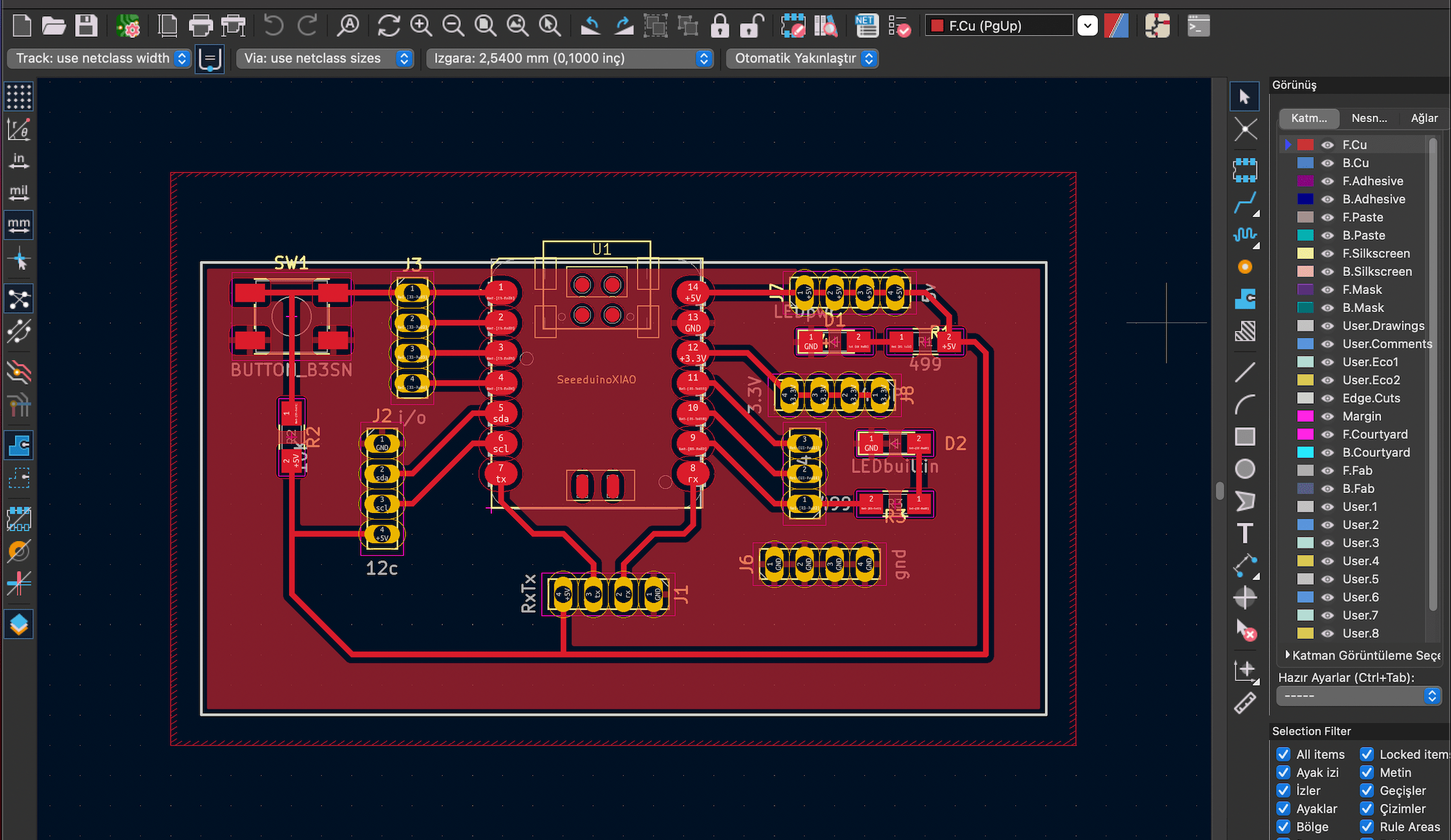
After completing the drawing, I transferred the drawing to the "Board Editor", where I edited the pins and the positions of the LEDs and connected them to the microcontroller. After making sure of the position and connections of all the elements on the board, I completed my drawing by making a frame for them.
2. Exporting
Before we could cut the PCB on the laser, I had to export the drawing I had prepared. To do this, I followed this path. File --- Fabrication output --- gerber file. Then, in the window that opens, Plot --- Generate drill file ---- Generate drill file.
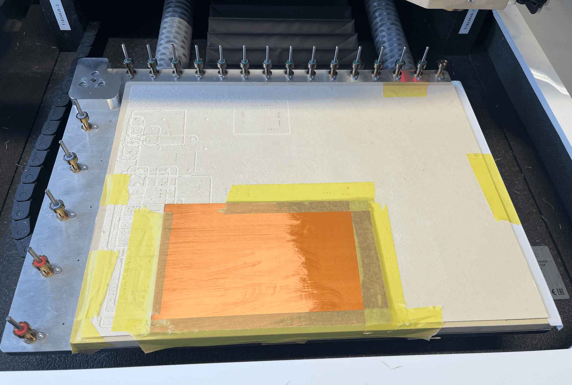
3. Milling
At FabLab Kamplinrfort we use the LPKF laser machine to create our boards. Before transferring my files to the computer, I placed the cutting board on the machine as shown in the image. I cleaned the protective surface of the board with the help of acetone and placed it on the machine by taping it between the numbers 3 and 10 of the machine.
I made the following adjustments on the software respectively;
- Choose templates as - single sided top
- Choose files and import
- Click on the icon that looks like a pinhole at the top left of the screen and open the "technology dialogue" page - copper layer thicknes: 35mm, isolation: 3 chanells.
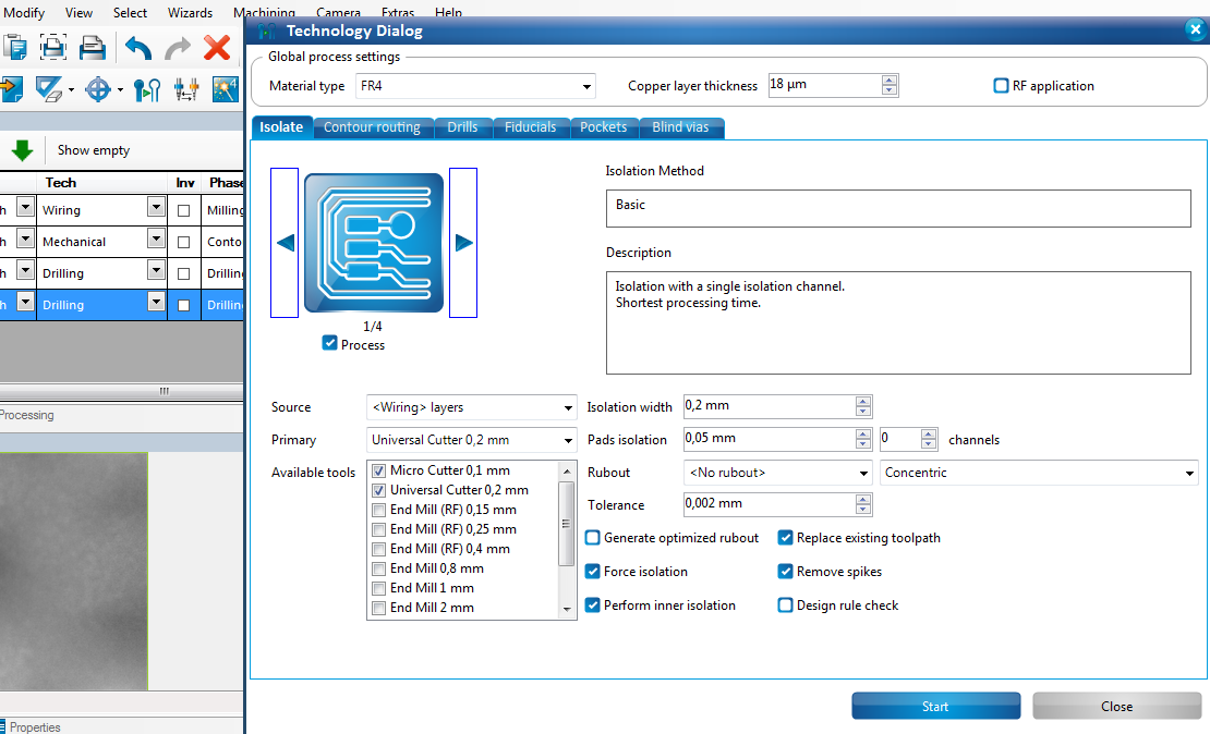
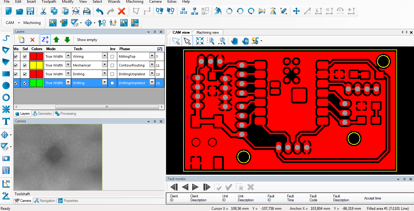
- On the main screen where I uploaded the files, I specified the data about which file will be cut and how. You can see this in the image below.
- To start cutting the board, click on the icon that looks like a magic wand and open the "Board production wizard"
- The machine will want to know where to start cutting, so use the interface to determine where to cob the cutter head and start cutting.
- I introduced the place where I placed the board in the Circuit Pro application and I completed the settings. Then I left the board to be milled.
For the tool-path generation and the machine setting, please check the group assignment.
4. Soldering
Before starting the soldering process, I found the necessary elements in the Lab. These were; 2 LEDs, 3 resistors, 1 Button and 1 microcontroller.
| Component Name | Purpose of Having |
|---|---|
| LED | For testing the microcontroller functionality. |
| Resistor | For connecting other commponents and cables. |
| Button | To control LED. |
| Seeeduino XIAO SAMD21 | Microcontroller |
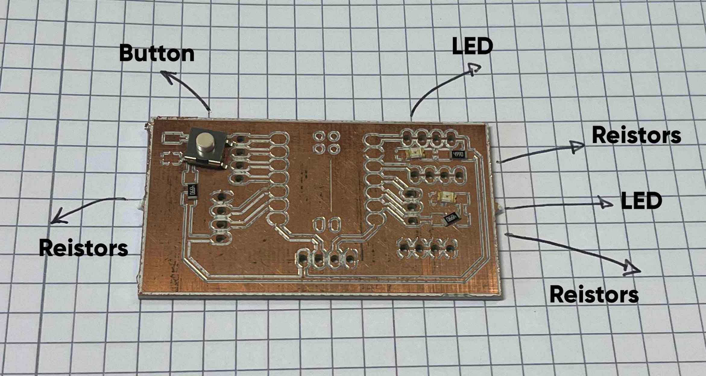
It was quite challenging for me to understand in which direction to place the LEDs. After learning that the place indicated in green on the back of the LED is catod, that is, the negative direction, and that the positive side should be close to the high voltage, I placed my LED in the correct direction. After deciding where all the components should be placed, I started soldering.
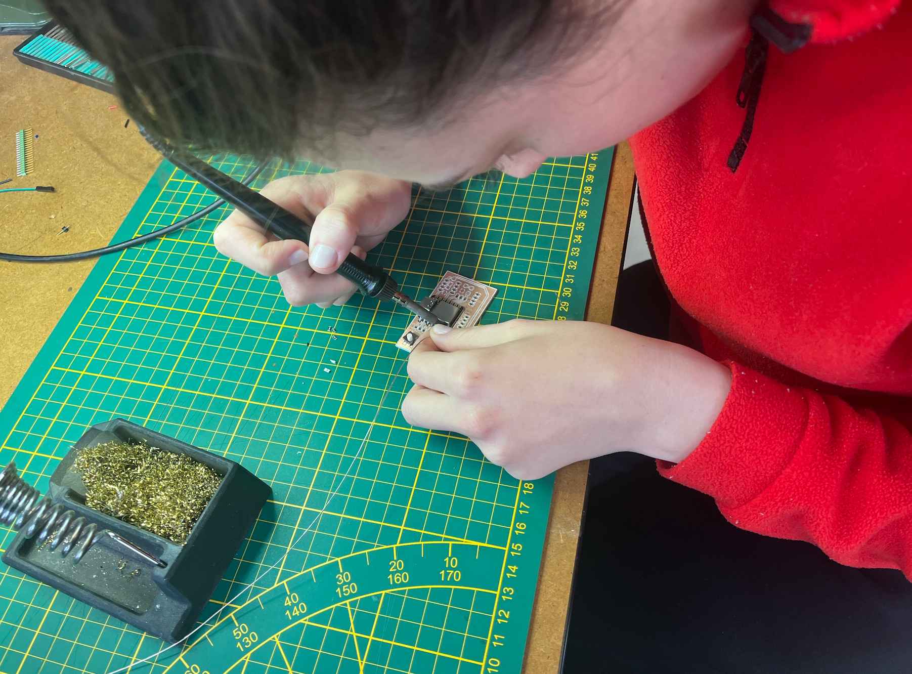
However, my instructor told me that I soldered the microcontroller incorrectly and soldered my LEDs in the wrong place. So we decided to remove them from their places. But this mistake of mine led me to learn new things. I used Solder wick to remove the soldered parts. We also used hot air to dislodge the microcontroller, but this caused the microcontroller cover to come off. We tested to make sure that the microcontroller was still working and looked at a PC and made sure that it was still alive after seeing the beam light up. This time after making sure of the location of the microcontroller on the board, I started soldering. I also repaired the cover of the microcontroller, soldered it and put it in place. After soldering all of the LEDs, buttons and resistors, my PCB was ready for soldering. But I was quite afraid of the test result because the resistors were very close and small and it was very difficult to solder them. Some places seemed to touch each other during soldering.
5. Testing
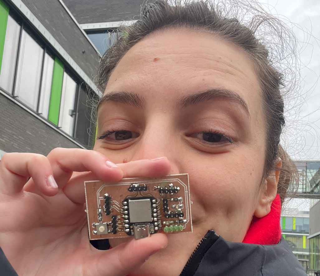
As I expected, the Arduino IDE gave an error and said that the port could not be detected. So I checked with my instructor what was wrong with the PCB with an ammeter. He told me that in order not to damage my computer, I should always first check the PCB for a short circuit by measuring it with an ammeter. I was lucky not to damage my computer! When we checked the PCB with an ammetre, we saw that there was a short circuit. When we found the problematic place on the PCB, we saw that there were places that touched each other in the solder and we soldered these places again. And It is working!
After when I was sure that it is still alive, for the testing part, I connected my PCB to my computer. I opened the Arduino IDE and I simply uploaded an example blink code to the board.
- Under the tools go to the port and find name of the microcontroller.
- Go to the file under the examples find the blink code.
- Change the pin number to communicate the LED of the pcb.
- To transfer the code, click to arow on the left side corner.
void setup() {
// initialize digital pin LED_BUILTIN as an output.
pinMode(8, OUTPUT);
}

// the loop function runs over and over again forever
void loop() {
digitalWrite(8, HIGH);   // turn the LED on (HIGH is the voltage level)
delay(1000);                       // wait for a second
digitalWrite(8, LOW);    // turn the LED off by making the voltage LOW
delay(1000);                       // wait for a second
}