8. Electronics design
Hero Shot
Group assignment:
-
use the Test equipment in your lab to observe the operation of a microcontroller circuit board.
-
send a PCB out to a board house.
Individual assignment
-
Use an EDA tool to design a development board to interact and communicate with an embedded microcntroller, produce it and test it.
-
extra credit: try another design workflow.
-
design a case for it.
-
simulate its operation.
it is the first time i will really try to design a board. i have try long time ago , that with fritzing to add on computer some electrique element and connect them. for sure it is amazing. for this job i will use Kicad, in version 8.

So for first download and installation. Kicad is free and we can get it in their web site. if you have some coins you can give them to support this good project. dowload kicad for windows x64
I had to go through a youtube to see some tutorial. watch video 1 eng; watch video 2 fr
For this assignment i work on my final project output board. so i will use XIO ESP32C3 board; my project is an 360 degre camera, with speaker and light. So for output i wille have:
-
1 led.
-
2 steppers motors and 2 ddrv8825 controlers.
-
1 speaker.
-
2 E2C ports
After installation you have

Then open a new project to start .
Libraries
Before working it is necessary to have library that content most of shematic symbol and footprint. mr Paul instructed us to clone the Fabacademy repository so that we get access to all the XIAO footprint and symbols to be used in our design.
is a link and steps to do that.
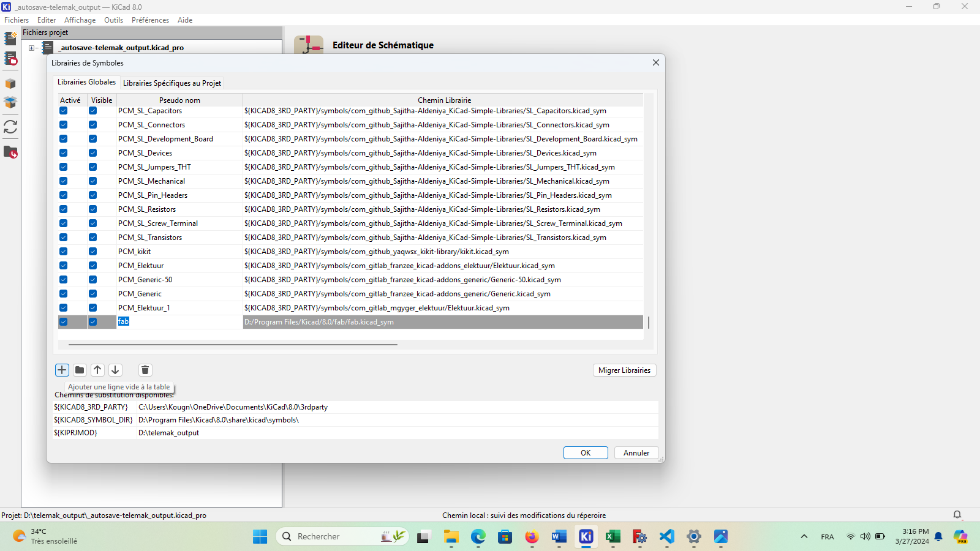
after that you need to go to preferences and manage symboles libraries and manage footprint libraries
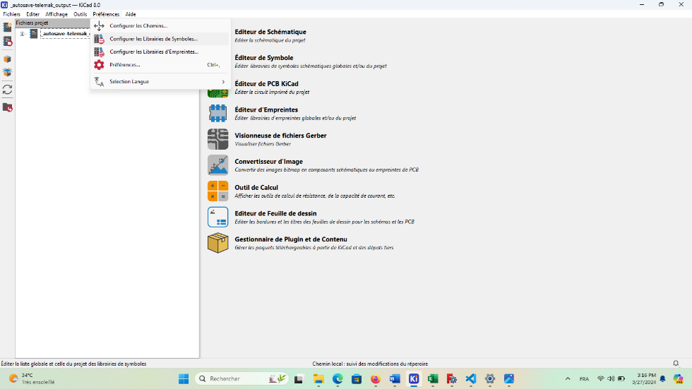
Click on “+” name the library and click to link the library you download on your computer. for me, i have some issue when i have not use the word “fab” and use it with upper letter “Fab”
Introduction to Kicad Schematic symbols
Start designing click on the schematic editor symbol below to open your schematic.
!
Then I started searching and placing components. To do that just click on the symbol below:

That takes you to the symbol libraries as you can see below. And there you can type and search for any component symbol you want. Scroll up and down to select from different components available on the list. Note that you can only pick one component at a time.

Once satisfied with the component Click OK at the bottom to get the component to your schematic. And just click anywhere on the schematic to drop it down. Highlight it and press M to move it and R to rotate it ino-rder to position it to its location. Press control D to duplicate the component if you want more of the same.
You can see the example how I placed components below.

So, to connect components together you can press on W on your keyboard to add a wire, or click on the Add wire symbol below on your schematic symbol editor.

Beow is an example how I have connected the components.

Anonother way of connecting components together is by using labels that can be used to name connection points.
To use labels simply press L on the keyboard or you can click on the I con symbol on the schematic shown below.

To join the components using net label flags you just have to name the connecting points with the same name eg. RR or LED LED. See below.

After connecting everything dont forget to click on electrical rules checker. It is also important to add power flags to our circuit as this helps the software to identify where the power is coming from. See below.

Below is how I have connected the power flag

Designing
So, for my design, I decided to use XIAO esp32 C3 Microcontroller for its wifi capability since in my final project I need wifi.
You can find esp32c3 specs here
Below is the pinout of esp32c3

Below is my schematic with all components connected.

PCB Editor
After finishing with the schematic click on open PCB in board editor symbol shown below.

And then click on update PCB with changes made to schematic.

Then finally you can start routing the traces.
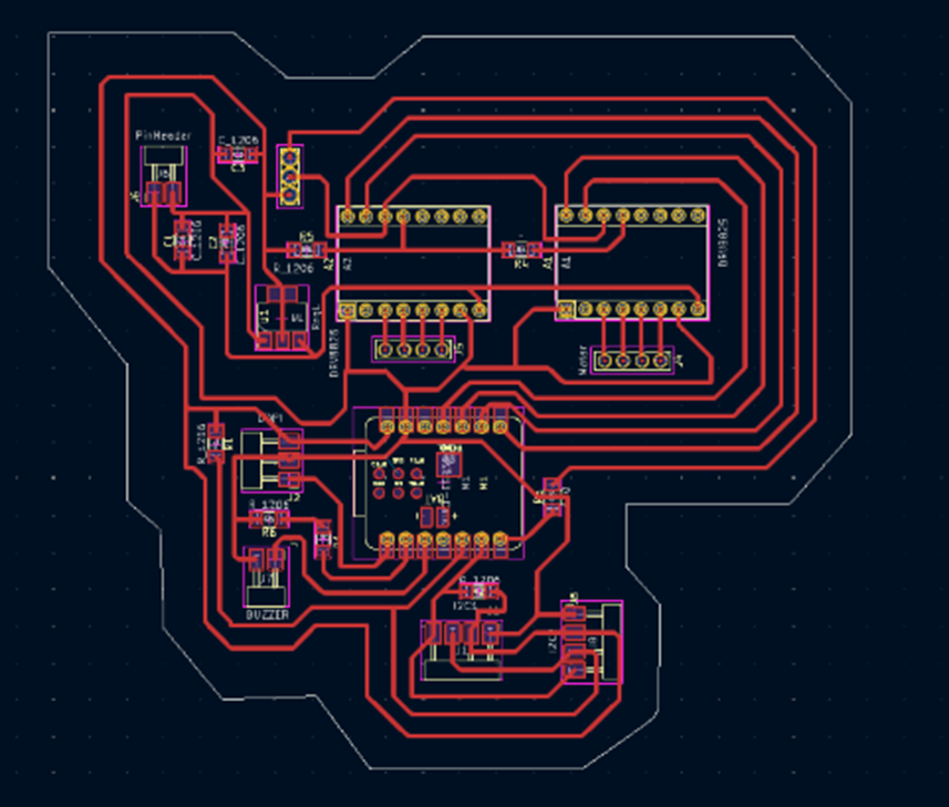
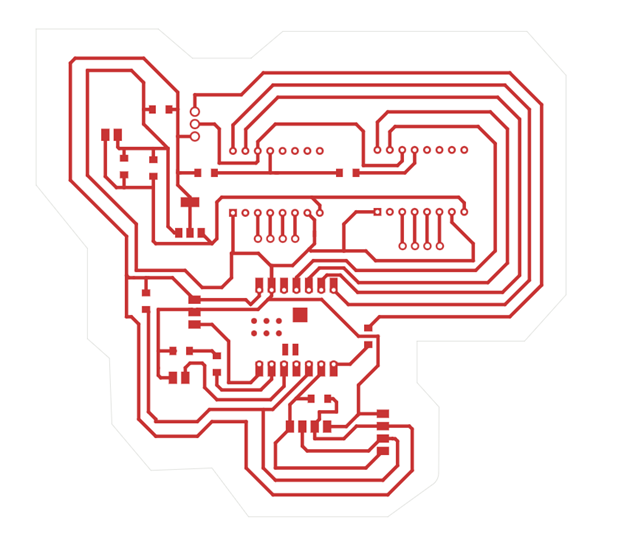
Below you can see how the circuit looks like after routing the traces in my Kicad PCB editor window with the components shown in my schematic.

You can click on view 3D viewer Icon on top and see it in 3Dmode as you can see below.

After being satified with the view I can export the file in gerber format for for further processing with a different software.
To do that, go to file>Fabrication Outputs>Gerbers(.gbr)
That will take you to this document below.

Click on plot to generate your F_cu and Edge_cut gerber file format. Remember to select the output folder for your gerber files. Then get back on the same document and click on generate drill File. That is excellon file for holes.

Below you can see I have generated gerber files. But there three important ones that I have circled. For copper traces, Edge cutting and holes. Those are the ones we are going to use for creating G-Code for the cnc machine.
Milling
To proceed with milling processes first we need to create G-Code for our machine.
G-code is a type of computer code that instructs machines on how to perform certain tasks. It is widely used in manufacturing and can control everything from the speed of a machine to the temperature of its heater.
FlatCam
A software that converts Gerber and Excellon (Drill) files to G-Code.
So, open your FlatCam software. Go to file>Ope gerber. That will let you import gerber files to to your flatcam project. And again File>Open Excellon to import the hole file.


For milling the Traces we used the following sizes.
Tool diameter = 0.33mm, tool depth = 0.08mm, Feed rate = 90mm, spindle speed = 1000, travel Z = 5mm, cut Z =0.08mm.

Then after generating the G-Code with FlatCam you export the G-Code for milling processes.