Week 4
Electronics Production
Fab Academy 2024
Riichiro Yamamoto
Dear My Friend
This week was the first week of electronic production. I was introduced to the making of PCB (Printed Circuit Board) PCB is a circuit board created by milling on copper board. Today, almost every electronic machine has a PCB inside.This week was one of the least creative weeks however it was an essential week to understand the basics of electronics. This week’s assignment was to make Quentorres, a PCB designed by Quentin Bolsee and Adrian Torres at Instructors Bootcamp for Fab Academy.
Hope you enjoy
Riichiro Yamamoto
Group Assignment
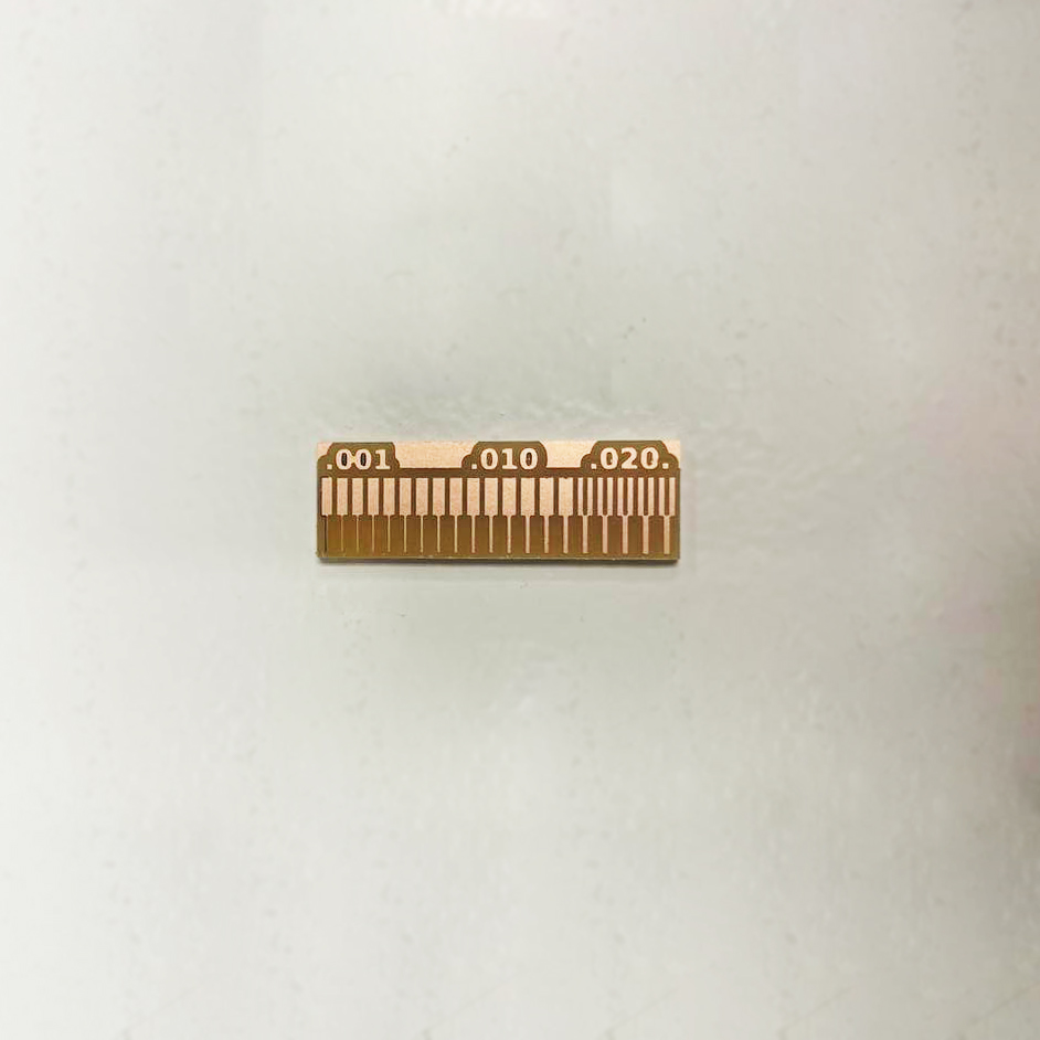
this week's group assignment was to characterize the design rules for your in-house PCB production process
Here is the link to the group assignment page
Prepare File
This week’s assignment was to make Quentorres, a PCB designed by Quentin Bolsee and Adrian Torres at Instructors Bootcamp for Fab Academy.
To prepare file for PCB milling, I simply used 3 PNG files prepared by Fab Academy, such as Trace, Holes, and Outline. Because it is a PNG file It is easy to edit with any kind of 2D CAD software. This time I put my name in Japanese as an additional design on the PCB. In general, the PNG file should only be Black and white since the black area is for cutting or engraving and the white area is for the circuit.
Files
QTtraces_withname_CUT.png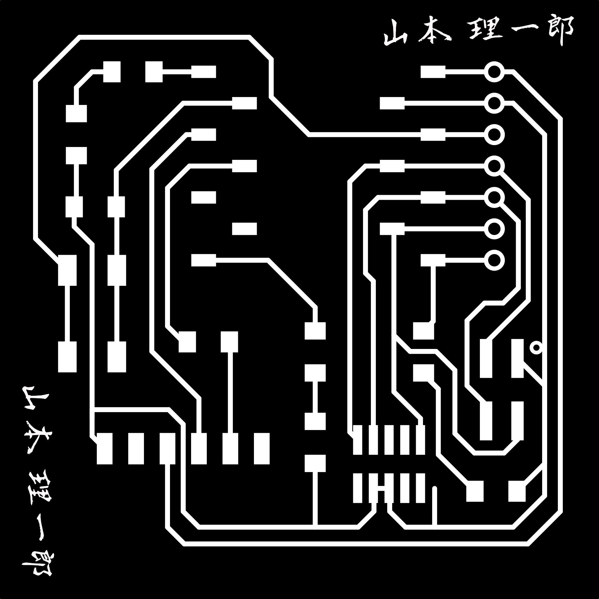
QTholes.png
QToutline.png


MODS
To convert the PNG files to files that the milling machine can read, I used MODS, software created by CBA at MIT and now sustained by Fab Academy. The workflow of using MODS is below.
Loading an image and program
- Open MODS: modsproject.org
- RightClick
- select program
- open program
- choose a machine (Roland Monofab PCB)
- get an image as PNG (no compression)
- read PNG
- select PNG file
- select file
- load image

Modifying data
upper parts are the transformation of the image (don't touch) use lower part to change values
- Set PCB default Tab
- choose traces(1/64) or outline & holes(1/32)
- Mill raster 2D Tab (generally no need to change)
- will load automatically
- check diameter depth, depth, max depth
- (set max depth to 1.75 for holes and outlines)
- offset number (4 is nice, 0 is to remove all the copper)
- offset step over 0.5 (no change)
- direction (climb should be fine)
- path merge
- Calculate


Set-up for the machine
- Machine Tab (Roland SRM-20 milling machine)
- speed 3 for traces, 1.5 for holes, 0.5 for outline
- Mill raster 2D Tab (generally no need to change)
- set xyz 0,0,0 (for holes & outline Do not change origin)
- check home Z (height) is above 0
- To Save file
- turn off the upper tab (this is to send it to the machine)
- turn on the lower tab (to save file in local)
- Calculate again Mill raster 2D Tab
- save window will pop up
- save in local folder
do this process for holes and outline
Files
QTtraces_withname_CUT.png.rml
QTholes.png.rml
QToutline.png.rml


Milling
Now the files are ready, it is time to mill the PCB. This time I used Rolad monoFab to mill the PCB. First I used double-sided tape to secure the board in the milling machine. At this point, it is important to place the board flat and straight because the milling is done on a scale of 0.1mm. If the board is not flat the machine will not mill properly.
Then I set XY origin by moving the milling head in the machine and set Z origin by dropping down the end mill carefully on the surface of the board. Finally, I chose my file and started milling. It is good to check whether it is producing dust as it is milling. If it's producing dust it means it is milling properly


Problem
My first trial for milling the board was a failure because half of the trace was not milled deep enough. This was due to the slight change in the angle of the surface when I placed the board inside the machine. When the board is like this, the circuit will not work properly because it is still connected to a thin layer of copper. Therefore I needed to try again.
The second time, the board was properly milled for most areas, but there was a small part that still had a thin copper layer, so this time I needed to remove the copper layer manually. I used a cutter knife and multimeter to check the connectivity while I removed the layer.


Soldering Set up
Before I solder I needed to gather all the components which I needed to solder for my PCB. By looking at the instructions of Quentorres I made a list of components and collected them from shelves in the lab. It was difficult to find each component just by its name, so I asked my classmate for help, and eventually, I was able to collect all of them. This process is very important because the soldering process should be done from small components to big components and from the centre towards the edge, so it is important to have every component beforehand to decide which components should be soldered first.


Soldering Enviroment
When soldering, it is good to have this kind of set-up below. The board, all the components, tweezer, soldering wire, soldering remover, multimeter, soldering iron, magnified glass, and soldering mat.

Soldering
Since it was my first time soldering, It took me a long time to get the soldering rhyme in my hand but in the end, I was able to solder most parts. However, the part I scratched to remove the unnecessary copper connection, the solder spread out and was not able to make it clean soldering.


Problem
After soldering I realized that I misunderstood the plantation of the microcontroller (XIAO RP2040) I was supposed to solder the socket (CONN HDR 7POS 0.1 TIN SMD) to the board but I directory soldered the the microcontroller to the board. This is problematic because in this way I will not be able to take out the microcontroller and use it for other boards. Also, this soldering was not connecting components so the board will not even work.
To remove the microcontroller, my tutor helped me. We used a heating plate and solder iron to heat up soldering and we successfully removed the microcontroller from the board.
Then I used a breadboard to secure the microcontroller and its legs to solder together, and also properly solder the socket to the board.
The lesson I learned from this mistake is that I need to have an image of how the components should be placed on the board before soldering and never solder components to the board if it is not aligned with the layout.


Function
To see if my PCB functions, I downloaded Arduino IDE which was prepared by Fab Academy, and connected my PCB. To connect PCB I used a USB cable and chose a USB port and the microcontroller in the software to make a connection.
To see my PCB function as it is programmed, I used the code written by my classmate. The code is simply programming the PCB to light up the LED when the switch is pushed. ( The code is below.) The result was successful. This time I used the code written by my classmate but I would like to learn how to write a simple code by myself.
const int buttonPin = D1;
const int ledPin = D0;
int buttonState = 0;
void setup() {
  // put your setup code here, to run once:
  pinMode(ledPin,OUTPUT);
  pinMode(buttonPin, INPUT_PULLDOWN);
  digitalWrite(ledPin,HIGH);
}
void loop() {
  // put your main code here, to run repeatedly:
  buttonState = digitalRead(buttonPin);
  if (buttonState == HIGH){
    digitalWrite(ledPin,HIGH);
  }else{
digitalWrite(ledPin, LOW);
  }
}


