8. Electronics Design
This week, it's all about PCB's and how to design them. On the bottom of this page you can see how i created my own pcb design, production and programming!
In week 4 we went through the production process of PCB's. Learned to create the .rml files in Modsproject and start the milling process of the traces and outlines + holes.
This week we learned how to design them and which components we need for the DEV board. We started with the software where we design the schematics. This software is called Kicad.
Kicad
Link to the software: download Kicad here.
In Kicad you can create schematic layouts which later on can get converted into a PCB layout. The schematic layout can be created by adding components (Press A to add) that have been added in the FAb library. Each component has the option to be labeled. This is an important step later for creating the PCB layout. If you want to connect one component to the other and the label that they have in common is a pinnumber, then they should both have matching labels with the same pinnumber.
Once the schematic is complete and all the components are labeled, the schematic can be converted into a PCB layout.
In the PCB layout, the main objective is to connect all the components their footprint to the matching components with traces. The challenge here is to connect all of them without letting them cross paths. To avoid crossing paths, I used resistors of 0 OHM to create a bridge.
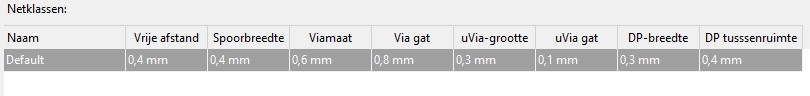
Some parameters had to be changed:
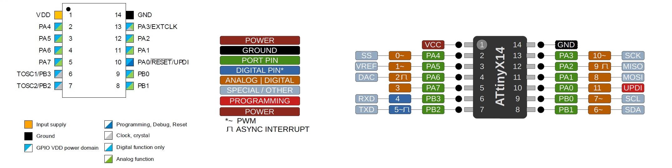
For this board I decided to use the ATtiny 1614.
This is the pinout:
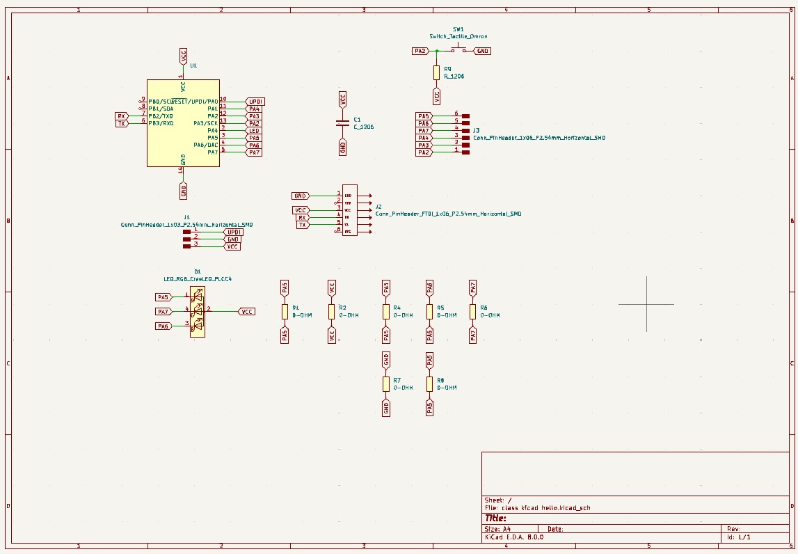
You can see in the picture below what a schematic layout looks like: this is the layout of the board that I designed.
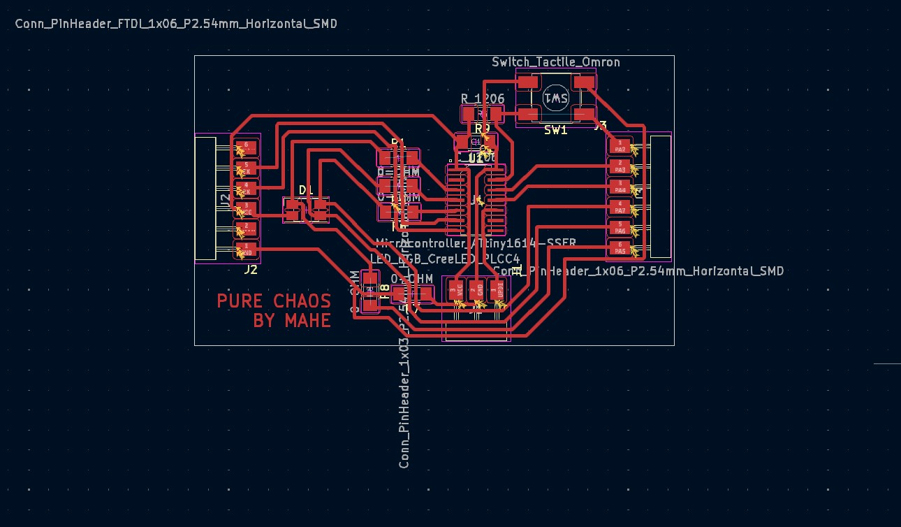
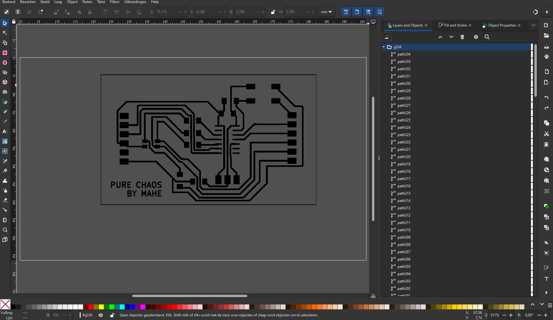
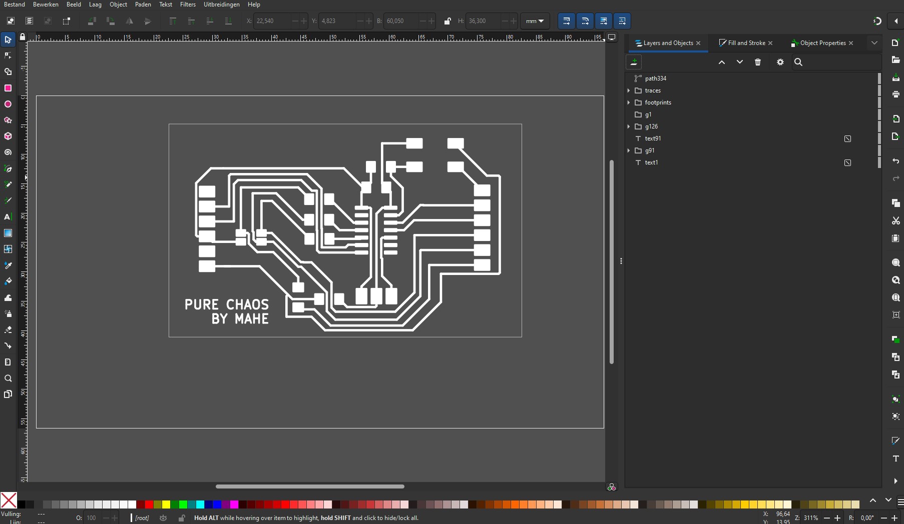
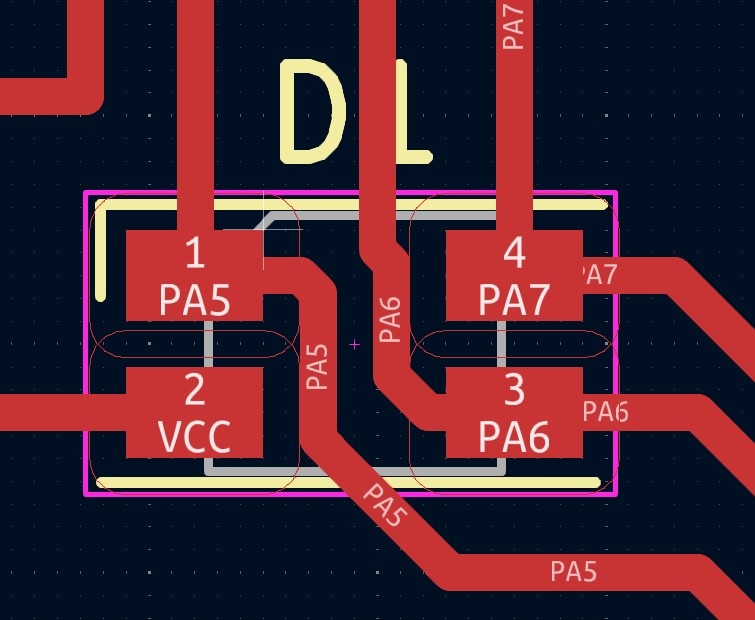
This is the PCB layout based on the schematic layout with the traces.
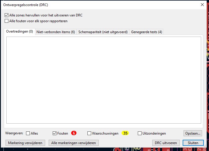
To check if everything is good and connected on the pcb layout, you can use a clearance tool that checks it for you. Here you can see errors or in my case now traces that are not connected.
Inkscape
When the PCB layout looks good and ready, it needs to be exported as a .SVG.
With the .svg openend in Inkscape, we can create a .png that later on can get imported in the modsproject to create the .rml file for the milling machine.
In inkscape you simply need to invert the colors from black to white , and white to black.
Modsproject
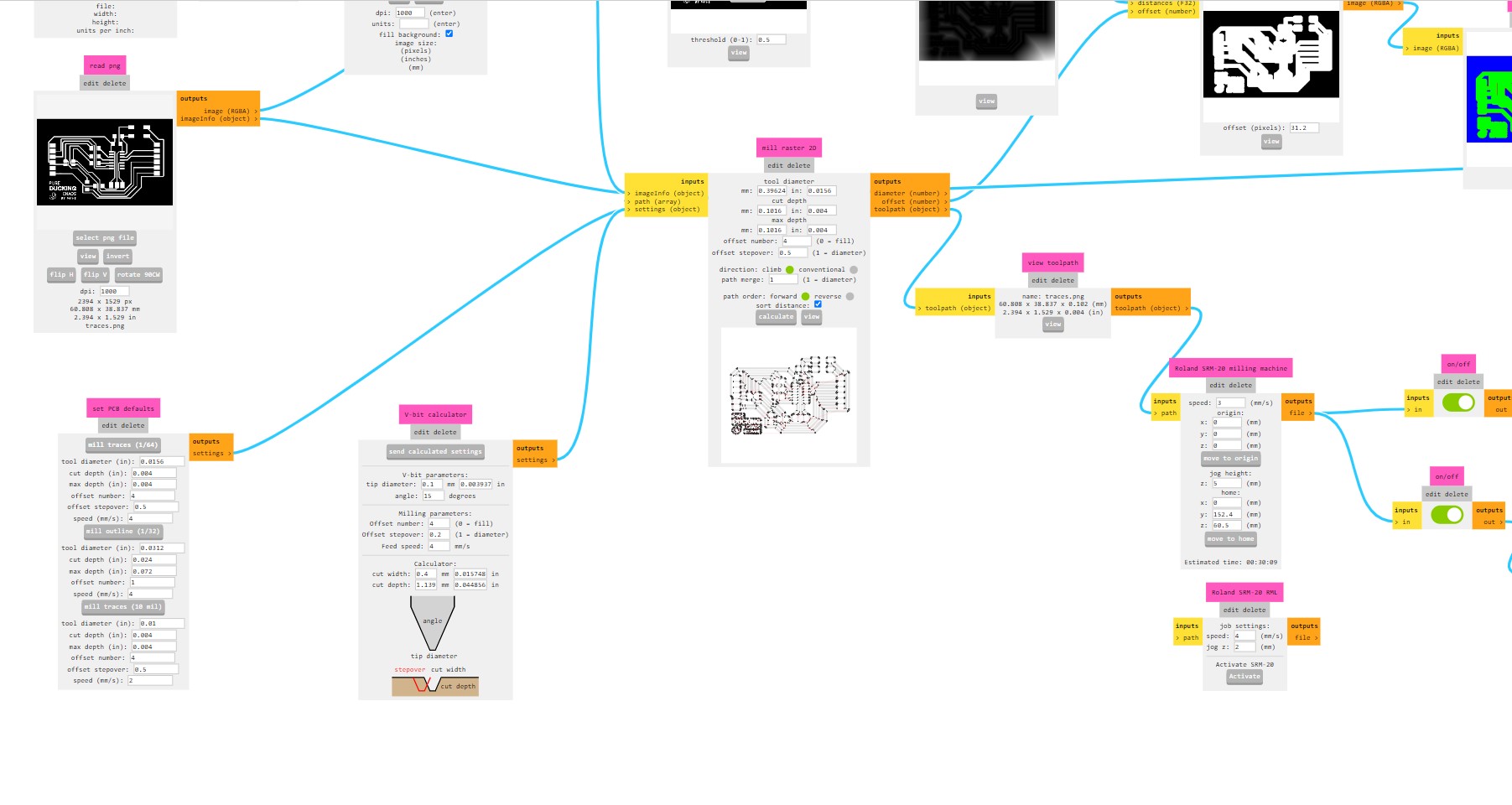
When the .png's are ready, they can get imported in the modsproject to create the .rml files for the traces and outline.
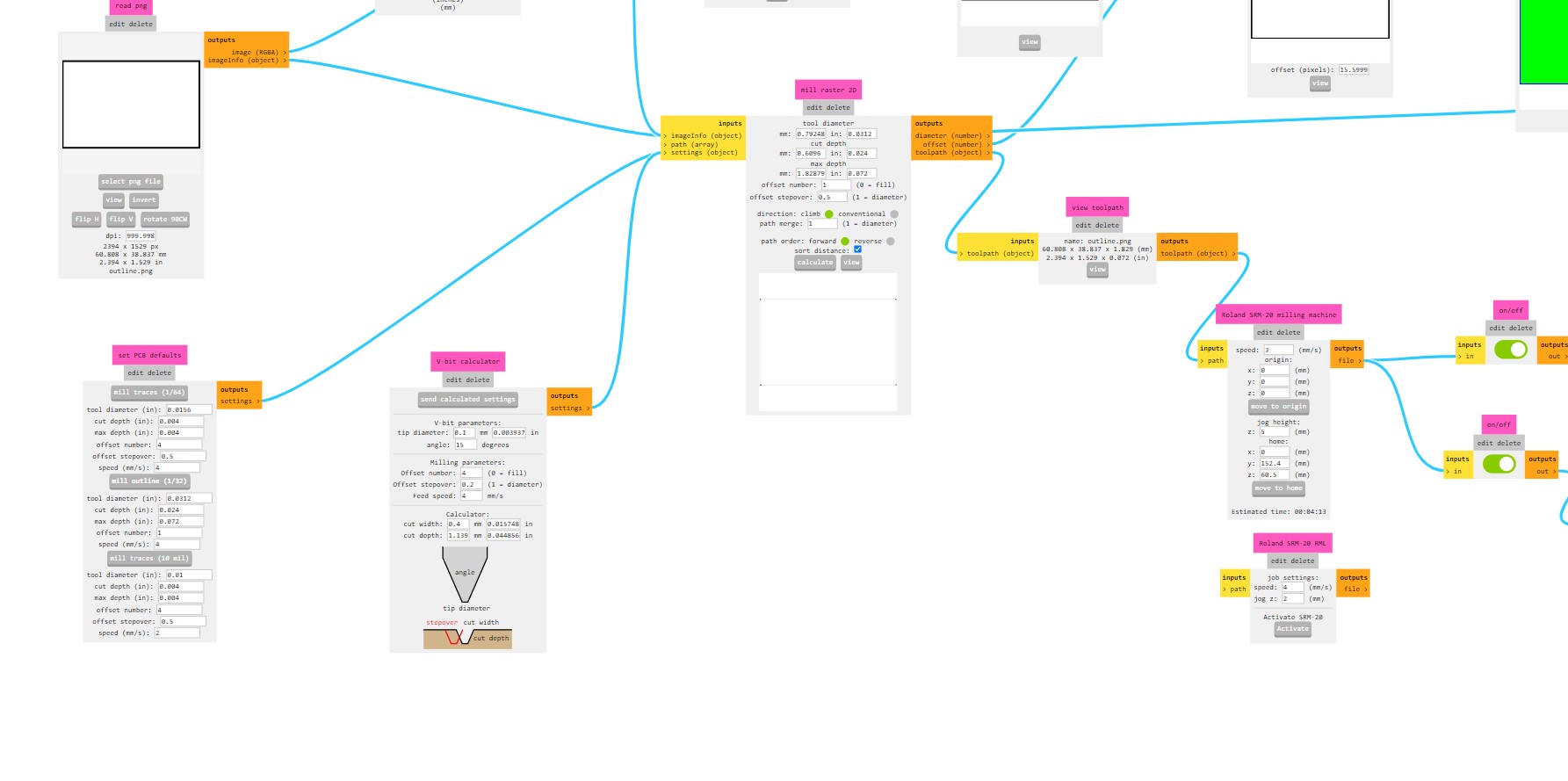
Milling
After milling, I saw that some traces were connected and should not have been connected. To fix this, I sanded the surface a bit and used something sharp like a cutter to erase some copper.
This is the LED in the PCB layout where I had 2 traces going through the LED. For my next design I now know that it is very tricky to have 2 traces next to each other that go through components.
This is the PCB with the problem.
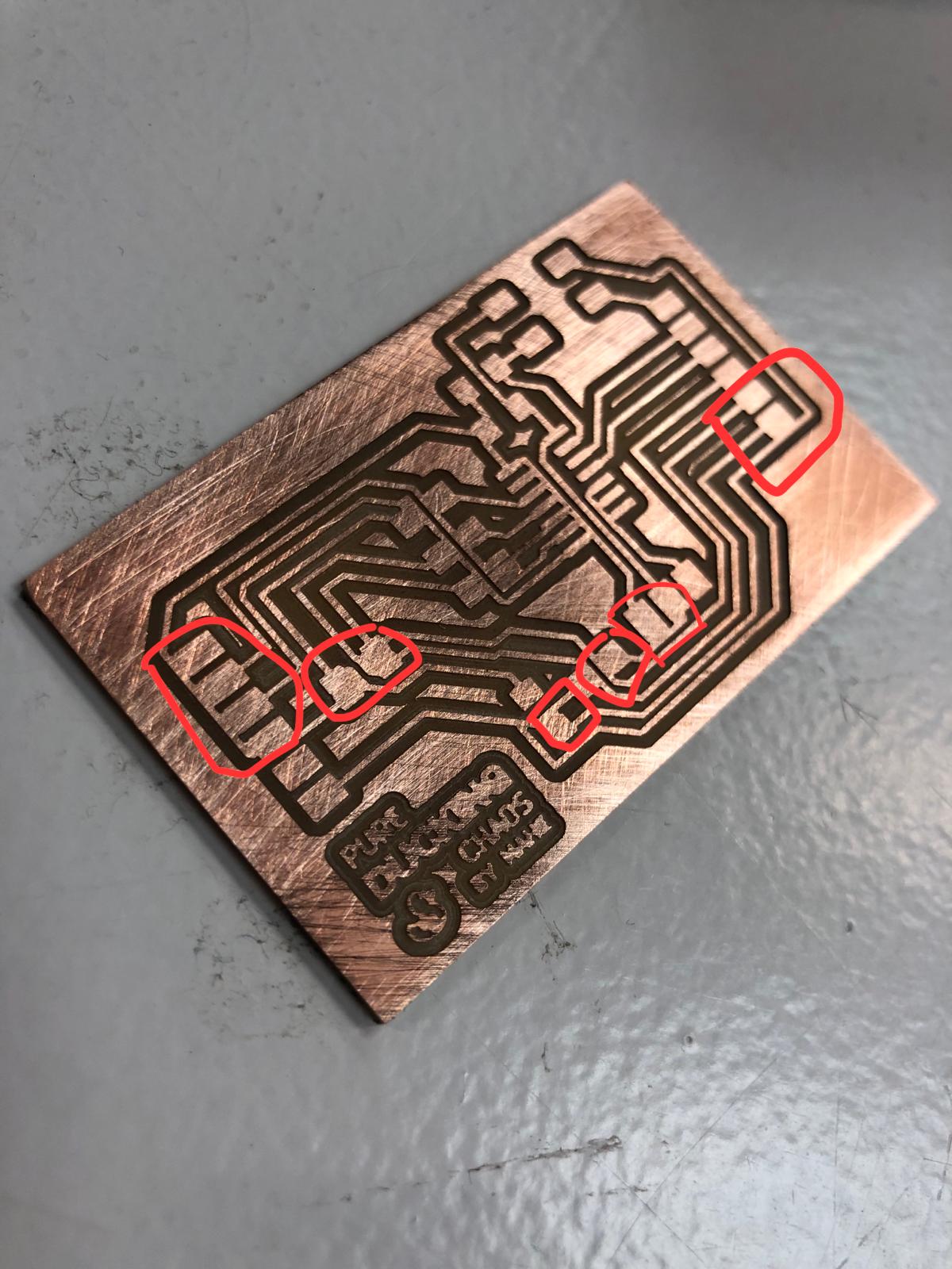
Fixed it using a cutter to clear the traces.
Soldering
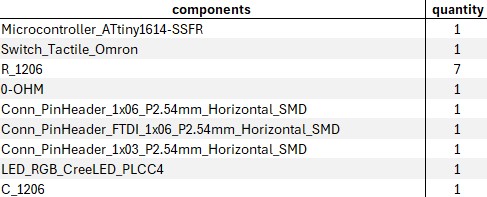
This is the list of the components I use:
(I know, lots of 0 resistors to jump... need to work on my puzzling skills)
Programming
I'm using arduino and the Seed Xiao board we made in week 4 to program this board.
As i'm using the ATtiny 1614, it's good to have the pinout sheet next to me.
This is the code I used in arduino to have the LED blink in a color when i press the button. Depending on the pinnumber i chose, i can chose the color of the rgb led.
With this code, the components like the button and RGB led can be tested.
- Pinnumber 1: red
- Pinnumber 2: blue
- Pinnumber 3: green
        // constants won't change. They're used here to set pin numbers:
const int buttonPin = 10;  // the number of the pushbutton pin
const int ledPin = 3;    // the number of the LED pin, in this case green

// variables will change:
int buttonState = 0;  // variable for reading the pushbutton status

void setup() {
  // initialize the LED pin as an output:
  pinMode(ledPin, OUTPUT);
  // initialize the pushbutton pin as an input:
  pinMode(buttonPin, INPUT);
}

void loop() {
  // read the state of the pushbutton value:
  buttonState = digitalRead(buttonPin);

  // check if the pushbutton is pressed. If it is, the buttonState is HIGH:
  if (buttonState == HIGH) {
    // turn LED on:
    digitalWrite(ledPin, HIGH);
  } else {
    // turn LED off:
    digitalWrite(ledPin, LOW);
  }
}
Final Result
My first pcb board from scratch
To create this board from scratch, I had the same process as the previously made board. Only difference is: this board works :p...
I'll just drop some screenshots of the files in kicad and modsproject and a video a the blink program.
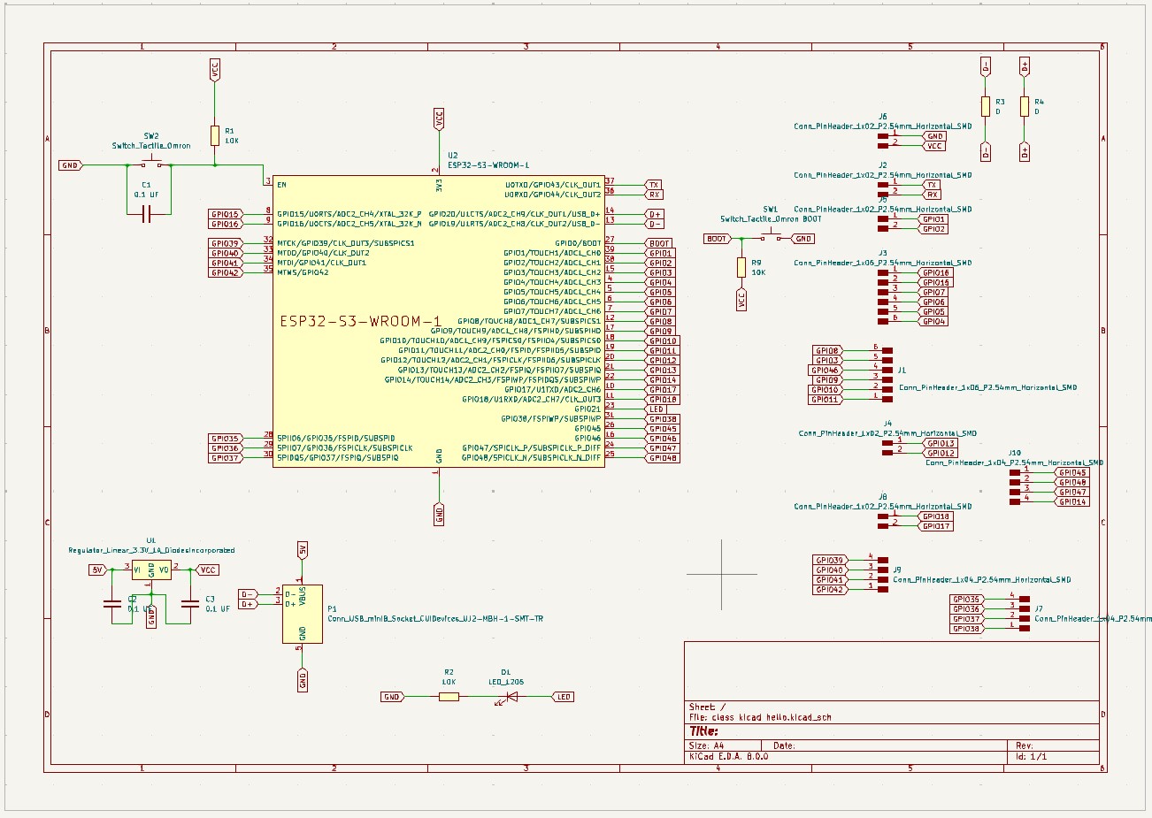
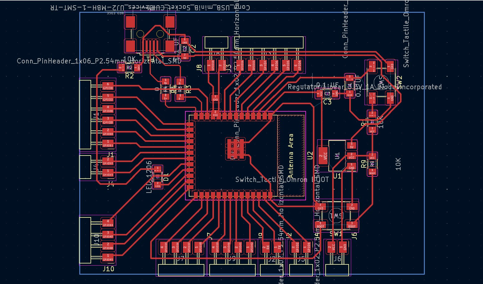
Kicad
The schematic and the pcb layout:
Note here that i made a mistake that i only found out later when the board was ready to be programmed: the ground circuit is not closed. To fix this i used a jumper to close the circuit.
Modsproject
To create the .rml files to mill the boards, I needed to create the 3 different .png files.
traces, holes and outline


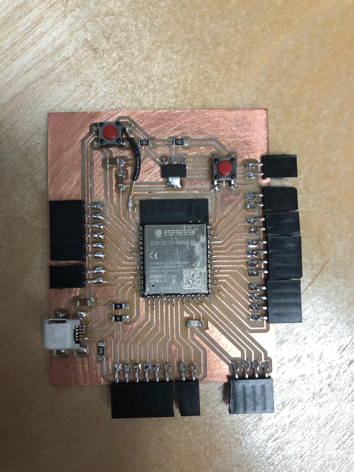
Soldering
Again, i did not take any pictures while soldering but this is the end result!
Programming
I used the blinking program to test the LED.
This is the code for the blinking program:
const int LED = 21;
// the setup function runs once when you press reset or power the board
void setup() {
// initialize digital pin LED_BUILTIN as an output.
pinMode(LED, OUTPUT);
}
// the loop function runs over and over again forever
void loop() {
digitalWrite(LED, HIGH); // turn the LED on (HIGH is the voltage level)
delay(1000); // wait for a second
digitalWrite(LED, LOW); // turn the LED off by making the voltage LOW
delay(1000); // wait for a second
}
video blinking LED
file
Group assignment
href="https://academany.fabcloud.io/fabacademy/2024/labs/barcelona/students/group-assignment/assignments/week08/"target="_blank">week 8