17. System Integration
This week we need to design and document the intergration of my final project.
Lecture Notes
Design steps:
- Conceptual - Think of the process
- Preliminary - Break down the steps and parts
- Detailed - Actual implementation
Dont go streight to detailed as it is not very flexible with change in design.
User experience & usability
- Simplicity
- Visibility & Feedback
- Current state
- Available Features
- How to access
- Natural Mapping e.g. up above down, left to right
- User Language - Clear symbols not words
- Avoid modes
- Principle of Least Surprise - It will act the way its 'expected' for most users
- Visual Design
- Itterative Design
Design for Manufacture
DFM optimizes the design of a product to make it easier and more cost-effective to manufacture.
- Use standard components
- Net shape - Processes that produce a part in its finished form
- Flexures > Fasteners > Adhesives
- Eliminate need for careful alignment - self aligning features
- Minimise parts
- Process selection
Documentation
Design Files available
Bill of materials used
Production - How to build it
Operation - How to use it
Packaging
How are PCBs mounted - standoffs, clips, insert mould
Route wireing
Align mechanisums e.g. Belt tension
Good surface finish
Testing
- Quality Assurance - defect prevention
- Quality Control - defect detection
- Burn-in - leave the system running to let components settle
- Cycling - Turning it off and on repeatedly
- Enviromental affect
- Fuzzing - Giving nonsense inputs
Failure Modes
How things can fail
Mechanical
Wireing failures
Components
Power
Software
Fail fast. Start early so mistakes can be learn from and be fed forward for next itteration. More effective than feedback development. Spiral developement.
Lifecycle
Right to repair. Disassembly possible.
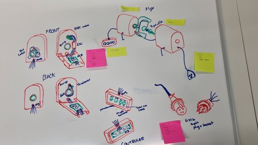
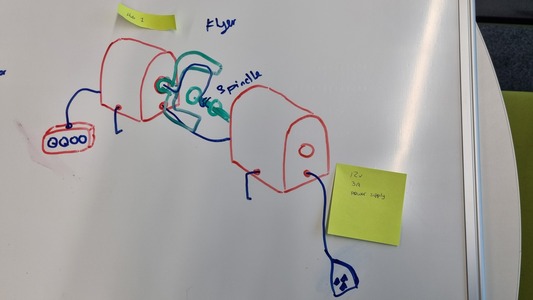
Final Project System
There are a few seperate sections to incorperate into the final project:
Front and back wall of nodes
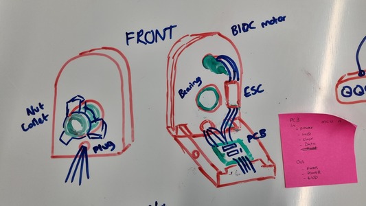
The nodes are going to be exact copies so they most work as both the first or second node in the chain. This means they will work depending on the I2C communication.
The front wall features the central hole which needs to run the entire length of the node and a place to install a plug for the wireing. On the inside face there will be a area for a 41.8mm bicycle headset bearing to be pressfit and a hole for the motor to be fit into. Due to how the motor is designed the connector wires come out the back of the body which means we need to allow space for the wires to come out beside the motor. The ESC will be mounted to the wall on this wall.
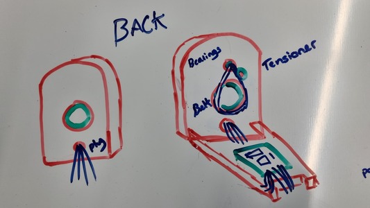
The back wall features the same centrol hole and plug hole on the outside. Inside there is a holes for two bearings and a threaded wool insert. The main bearing goes in the back of the central hole. A smaller bearing supports the motor to make sure it is not pulled inwards by the belt. There is then a hole to fit a m5 threaded wood insert which the belt tensioner will attach to. Different heads can be fit to provide the best tension.
Base of nodes
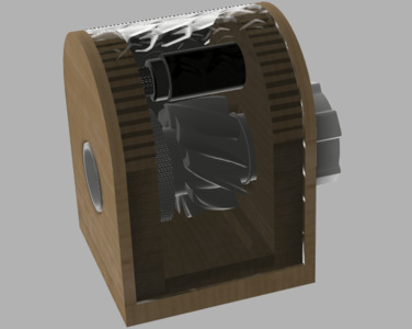
The base will be shaped so that it is flush with the walls. There will need to be a milled gap on the inside which allows the wires from the plug to come in from the back and front wall to the PCB which will be fastnend down to the base using threaded wood inserts.
The base will be joined to the walls by countersunk bolts that will screw into the base. The otherside may be glued in place so the bolts are not visible on the front face. The base needs to part from the walls so that you can take out the internals.
Shell
The shell is made from a wool-resin composite that is moulded to the shape of the front and back walls. The walls have cutouts which alows the shell to overlap and sit flush. The shell will be fastened to the base using small magnets.
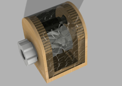
Inner workings, gear assembly, ESC and motor
The inrunner bldc motor has a standard GT2 6mm idealer drive pully, 20 tooth and 3mm bore.
The estimated belt required is 92 tooth (184mm) GT2 6mm belt
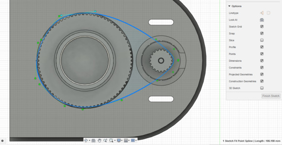
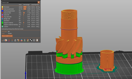
The barrel which allows the attachments to move all the way through the node will be 3D printed and include the other GT2 pully. It also has some fan blades to keep air moving within the node for cooling. There are also bearing stocks which just press against the inner race of the bearings to keep them in place. The barrel has a large thread and a taper at that end for the collet system.
Tools
The bobbin will slide onto a 8mm aluminium knitting needle. The current plan is to have a 3D printed bobbin which has unscrewable ends and feature TPU ends which will grip the needle.
The needle is held in place using a collet which slides into the end of the central barrel and gets tightened down using a nut.
The flyer will screw onto the same thread as the nut and allow the spin wool through the center and up to wool guides.
I still need to try out different designs for sliding wool guides, possibilt encasing the ball bearings within the print.
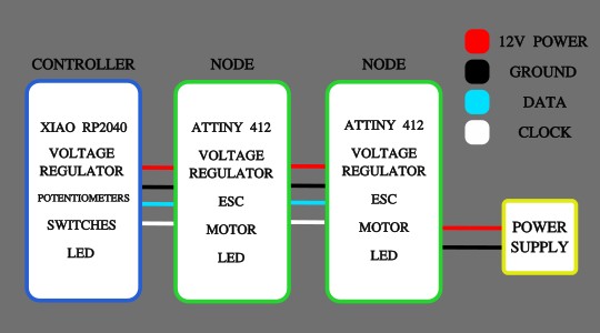
Controller
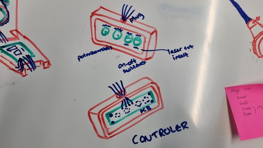
The controller will have two potentiometers and two rocker switches. The potentiometers will control the speed of the spin and the second will change the difference in speed between the forward and 'break' motor.
The outside of the controller will be milled and the front face may be laser cut, this depends on how well the switchs and potentiometers clip on.
The PCB within the controller will also have a Xiao RP2040 which will be the main controller for the I2C protocol.
The PCB will be attached inside the controller using wood threaded inerts and standoffs to have the inputs be held at the correct level.
Wireing
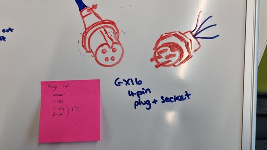
The connectors I will use for the cables running inbetween the nodes and the controller are gx-16 4pin aviator connectors. I find these connectors appealing to be visible on the outside of the parts. They are also keyed so connot be plugged in backwards as well as having a screw coupling so keep them securely inplace.
I will be using 21 AWG wire as that is more than enough as its maximum amps for chassis wiring is 9Amps, we did not go over the 3Amp max of the benchtop power supply we used to power the motor during machine week. The block terminal that I will use to connect the wires to the PCB works for gauges 22 to 14AWG.
Finally to make it aesthetically pleasing and hide the colours of the wire I will be using paracord to keep the wires together.
The wires will be running 12v power, GND, SDA (Serial Data line) and SCL (Serial Clock Line).
PCBs
There will be two types of PCB: one for the main controller and one for the nodes.
Main PCB
The main PCB will be in the controller and its microcontroller will be a RP2040.
There will be analogue inputs from two dile potentiometers and two digital inputs from switches.
There will be a block terminal that will take the wires from the connector. The 12v line will go through a 5v voltage regulator which will be used to power the rp2040.
There will be one LED indicator light to show the machine has power.
For I2C the data and clock lines need to have a pull up resistor each in the range of 4.7K or 10K ohms. The pull-up resistors provide a high level on the lines when none of the connected devices are driving the bus.
Node PCB
The node PCB will have a ATtiny 412 as the microcontroller.
There will be two block terminals for the wires to enter and exit the board from.
There is a 5v voltage regulator for the 12v line.
The ESC requires banana plugs for the 12v power and GND to be fed forward. It also has a 3pin connector for the PWM and GND information signal.
There is also a indicator LED.
Code - I2C
I had originally planned to use wireless networking but as we are already needing to run power and ground between the notes we might as well run two more wires for I2C and it avoids the problems of having to connect all the parts and running a broker.
The controller will have the main microcontroller and the nodes should be the ones following the orders. Ideally the nodes can be connected in any order as they are identical and depending on which way round they are connected they behave differently.
There are two types of node: the first will have the input of the wool and the flyer will be attached to it, the second will have the bobbin and knitting needle and be turning slightly slower than the flyer. The amount or break affects the amount of twist in the wool so it needs to be adjustable in relation to the speed.
Note most I2C information is taken from the RP2040 Datasheet
The I2C protocol involves using two lines to send and receive data: a serial clock pin (SCL) that the controller board pulses at a regular interval, and a serial data pin (SDA) over which data is sent between the two devices.
The master is responsible for generating the clock and controlling the transfer of data. The slave is responsible for either transmitting or receiving data to/from the master.
When a master wants to communicate with a slave, the master transmits a START/RESTART condition that is then followed by the slave’s address and a control bit (R/W) to determine if the master wants to transmit data or receive data from the slave. The slave then sends a acknowledge (ACK) pulse after the address.
RP2040
The I2C standard requires that drivers drive a signal low, or when not driven the signal will be pulled high. This applies to SCL and SDA. The GPIO pads should be configured for:
ATtiny 412
To enable the TWI as Slave, write the Slave Address (ADDR) in TWI.SADDR, and write a '1' to the ENABLE bit in the Slave Control A register (TWI.SCTRLA). The TWI peripheral will wait to receive a byte addressed to it.