4. Electronics Production
This week we are looking at ways you can produce electronics.
Etching
Etching is the process of removing the excess copper from a board through chemical means. The traces are protected by a film or material which is resistant to the chosen chemicals. This is lots of water waste from this process and the handling of dangerous chemicals is not ideal for a lab. However, this process is commonly used by board houses and electonics companies as it is fast and efficient when making in bulk.
Milling
Millng invoves machining the excess copper away using CNCs. This is good for fast prototyping a board, however slow in bulk.
Vinyl cutting
The vinyl cutter can be used to cut traces out of copper tape. This allows for flexible pcbs, however the traces are delicate and require weeding.
2024-02-14
Here are notes on the topics Niel covered today.
In order to create PCBs CNC milling is one of the most common for labs. However, vinyl cutting is also a viable method.
The CNC mill uses tool bits to cut through the copper. The most common types are:
End Mills
V-Bits
In our lab we normally use end mills, however I will be trying out v-bits to see how they compare as part of the group project.
Underlay is a piece of waste material which lies between the PCB and the bed of the machine. It provides support to the board, not a issue if you cut through it, but does get used up over time. Although not quite the same as underlay, we use some plywood under the pcb in order to raise it up off the metal base.
Fixturings connect the PCB to the machine bed, ensuring it doesn't move under the force of the milling. There are various ways of doing this such as clamps or tape. For PCBs we use a sandwitch of tape and superglue. This allows for easy removal whilst fastening the board down firmly. This also means tabs are not required when cutting out the board.
Zeroing tells the machine where you wish the machining to start in the X-Y directions. It is important to not change the X-Y zeroing if you have multiple machining steps as do that will cause missalignment. In the Z direction it tells the machine where the top surface of the board is. It will mill downwards from here the amoout that is specified in the g-code. You can zero the z direction by using a probe or, once the head is close, loosening the tool so its tip touches the surface of the PCB.
After the milling is complete you may need to de-burr the surface of the pcb. This can be caused by a tool bit that has been dulled from use or missalignment in the bit. In most cases you can clear this up by scraping with a sharp metal edge and some wire scouring pads. The tools do have a limited lifetime, but is longer than expected as long as the points do not snap.
PCB board come in different types. FR-4 boards are glass reinforced and are not sutible for machining. FR-1/FR-2 are copper clad and machines well.
Machining the boards allows for fast prototyping of components, however can be a lengthy process if you want to mill out large batches. Once you can gone past the prototyping stage it is advised you use a board house to produce the PCBs in batches. There are many board houses, some of the big names or PCBWAY and JLC PCB. These companies provide a wide array of options such as multiple layers, silkscreen designs, different materials and colour options and pick and place services. I ordered a PCB through JLC PCB you can read more on our Group Page.
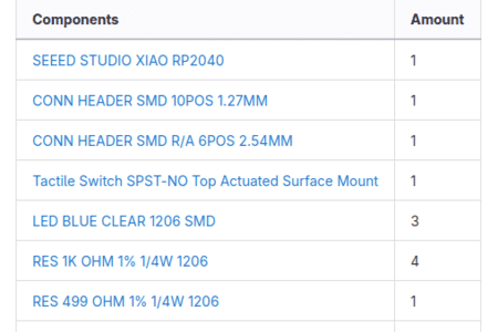
Components are available in different footprints and sizes.
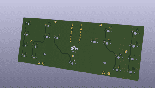
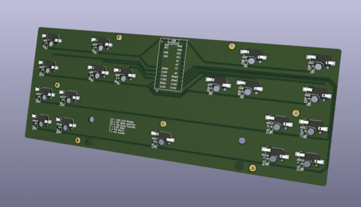
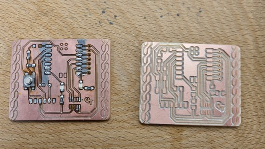
Redisigning the Quentorres PCB
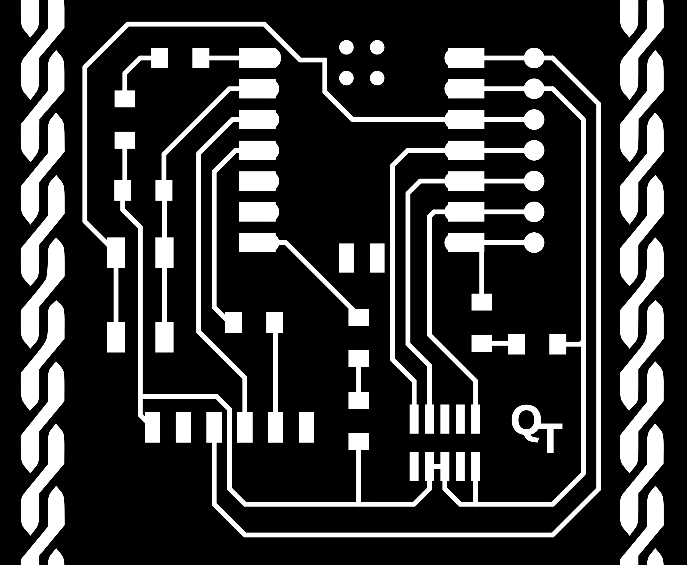
I went and downloded the PNG files from the Quentorres GitHub page. I chose the version where the Seeed is soldered directly to the board.
I initially considred changing the shape of the board, however didn't want to increase the footptint of the board too much. I decided on adding a pattern to the board. It needed to be a relitivly simple design that could be milled successfully.
I ended up with a twisted boarder design.
I opened up the original design PNGs in Inkscape along with the chosen pattern. Increased the size of the document and centered all the layers of the PCB so that they would be perfectly inline.
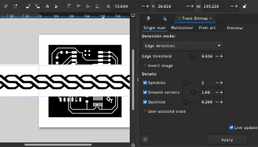
I traced the bitmap in order to get a vectorised version of the pattern that would have cleaner edges and could be altered easily by using the nodes. The trace provided the black outline while i was looking for the white sections as that represents the copper which is preserved. To fix this I roughly drew a background shape to fill in the gaps then grouped them together. I also cleaned up some extra points.
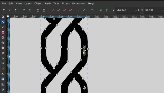
I duplicated the pattern on both sides then drew up a new outline cut file with soem fillited corners. I then made the document size slightly larger than this line. It is important the images are exactly the same size so that that it lines up when you come to the machining.
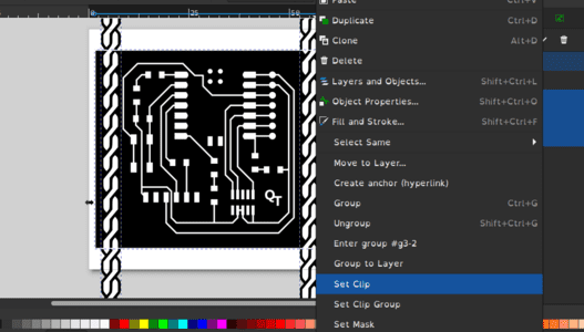
Using a rectangle the same dimensions of the board I set it as a 'clip mask' to crop the extra design so that it no longer overlapped.
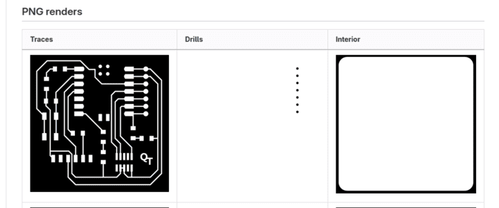
I then exported all the files: traces, holes and outline. I initially exported at 300 dpi, however I remembered incorrectly. The files need to be exported at 1000dpi so that when it comes to creating the gcode it has enough quality to create nice lines and curves true to the design.


You can download the inkscpae svg by clicking below.

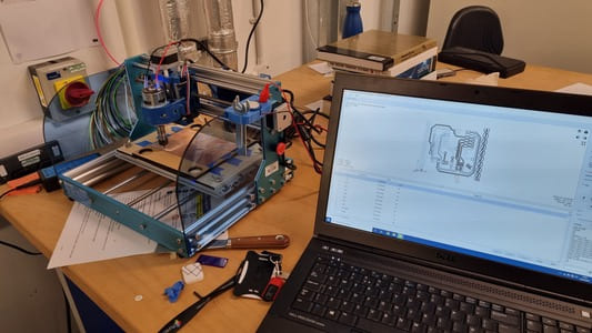
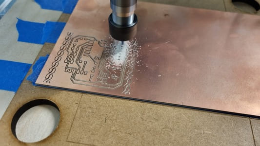
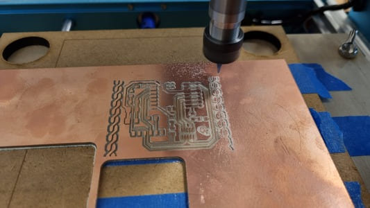
Milling the PCB
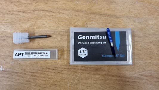
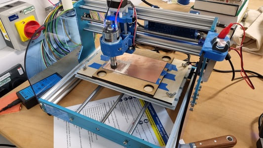
Following tests on both our PCB Milling machines, Roland SRM-20 and 3018 proVER, I decided to use the 3018 proVER with a v bit to mill out the board.
.jpg)
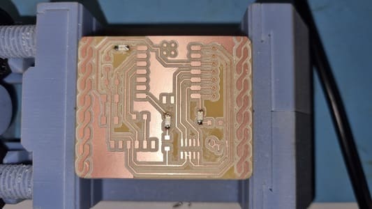
I loaded a new FR-2 copper sheet onto the machine using the superglue and tape method and loaded the v-bit into the collet.
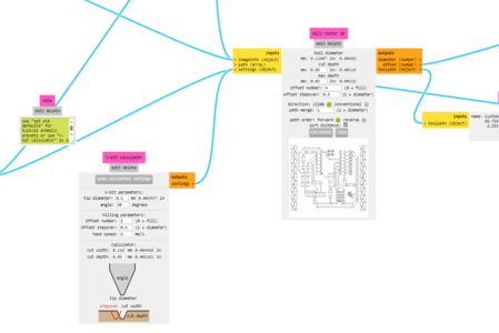
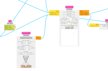
I used mods project to create the gcode files.
It is useful to remember that copper is the white in the PNGs, the milling will preserve the white areas.
Traces
Cut/Holes
It generates a preview of the files which is very usful to spot mistakes such as the image needs inverting (milling out the traces instead of around them) or the PNG quality is too low (milling path looks angular and jagged).
I open Candle which is the gcode controller for the 3018s. Use a probe to zero the z axis and move the tool to the bottom left corner of the area i want to cut within to zero the X and Y axis.
I use 'open' to load the gcode for the traces file. I then start the machining by pressing 'send'.
VIDEO
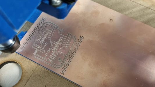
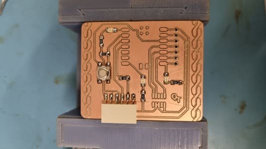
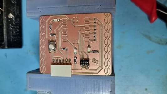
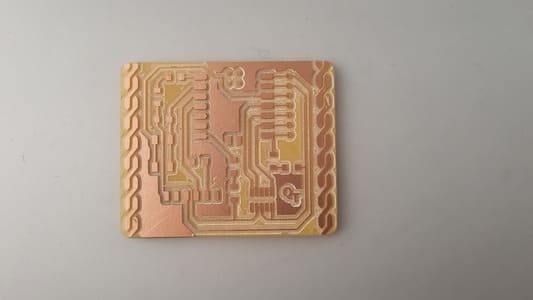
The traces took about 40mins to mill out as the speed was resonably slow and the decorations added more complexity to the design, but I was very happy with the result.
I vaccumed any dust it created then started the holes milling file and afterwards the cut out file. These took a couple minutes each.
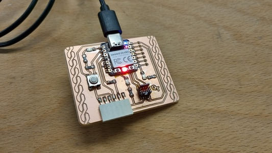
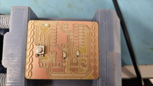
The PCB it created was very clean and did not require any deburring. The only issues were that everything was slightly deeper than needed. This cased the v-bit to take away a bit more material than intended due to the tapered shape. This was mainly a issue with the holes as it removed too much copper to be a good pinout area.
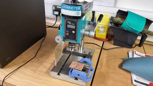
We planned to fix this by increasing the holes to 1mm using the piller drill and then soldering some pin head connectors to the board permanently.
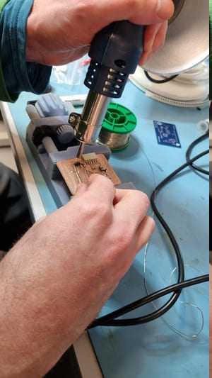
Soldering
I started by collecting all the neccessary components for the board.
In order to solder surface mount components you need to clean and tin the soldering iron to ensure it is shiney.
Place solder on one of the pads of the component.
Hold the component with tweezers. Reheat the solder and slide the component in.
Remove heat and allow solder to solidify.
Solder the other side down by heating up the pad, dabbing the solder until some melts off onto the pad.
Check that there are no bridging occuring to prevent short circuits.


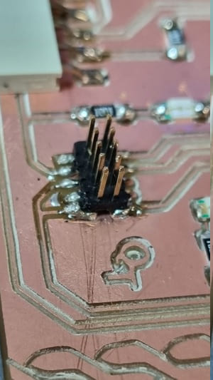
The pads were very close together making this the hardest component to solder down. On my first attempt the solder went around the end. John helped me desolder the pin header using hot air and solder whick. The second attempt was more successful, however it was very difficult to only put the minimum amout on the pad. I'd expect reflow using solder paste would be better suited here.
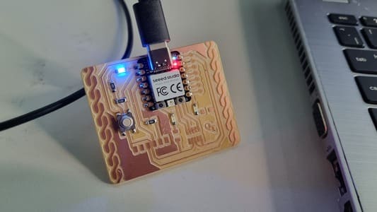
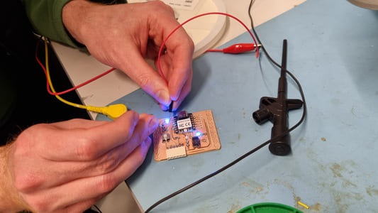
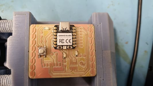
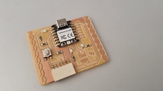
I then finished by putting on some kapton tape on the back of the seeed to protect it from short circuiting and soldering it on.
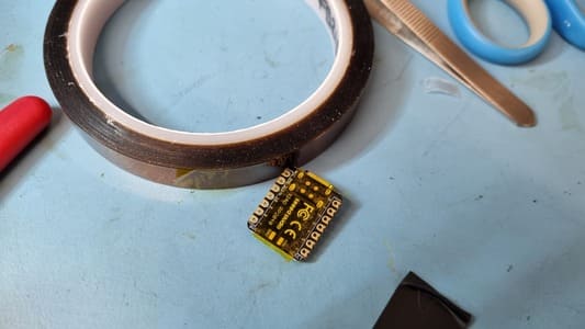
The seeed lights up successfully after plugging it in.
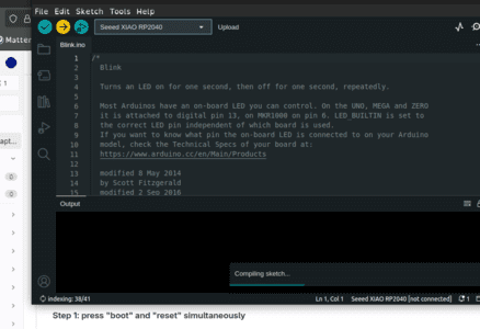
Basic coding using Blink
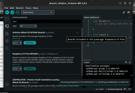
I downloaded the Arduino IDE from it's website.
I followed the instructions on the quentorres github. In order to install the correct libraries.
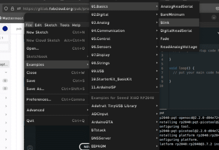
I used the base code from the example blink tutorial.
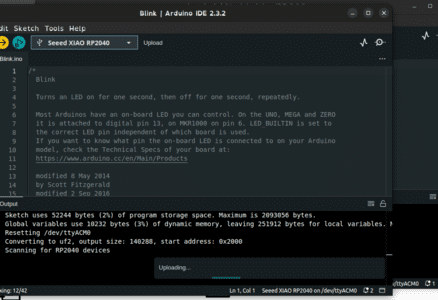
In order to connect my seeed I can to put in into boot mode by holding down the small 'b' button whilst plugging it into the computer. It shows up as RPI-RP2. We then click verify and upload to send it to the board.
I used the following code:
int LED = 26;

void setup() {
  pinMode(LED, OUTPUT);
}

void loop() {
  digitalWrite(LED, HIGH);  // turn the LED on (HIGH is the voltage level)
  delay(1000);              // wait for a second
  digitalWrite(LED, LOW);   // turn the LED off by making the voltage LOW
  delay(1000);              // wait for a second
}
Troubleshooting
Initally my board had some mistakes. The code didnt work for the LED on pin 26 but did on pin 0.
After some testing with the osillascope to check the LED still works.
We tried with some lower ohm resistors incase the design was wrong, however this did not solve the issue.
We made a breakthrough with the multimeter that showed I had a short probably over pin 26's LED. In the process of removing we accidently broke off the delicate trace.
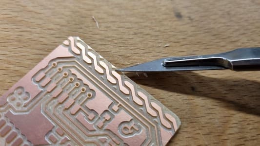
I salvaged the seeed from the board and then milled a second replacement PCB. This time I decided to increase the offset number from 4 to 8 to avoid having any copper which could be accidently soldered to.
I then removed any extra copper by hand with the help of a scalpel.
Resoldered the board
Tested the LED code and it worked perfectly this time.