8. Electronics Production
The assignment this week is to characterize the design rules for our in-house PCB production process, make and test the development board that we designed to interact and communicate with an embedded microcontroller. For extra credit we could: make the board with another process and send a PCB out to a board house.
Board Design/MIT Mods Convertion
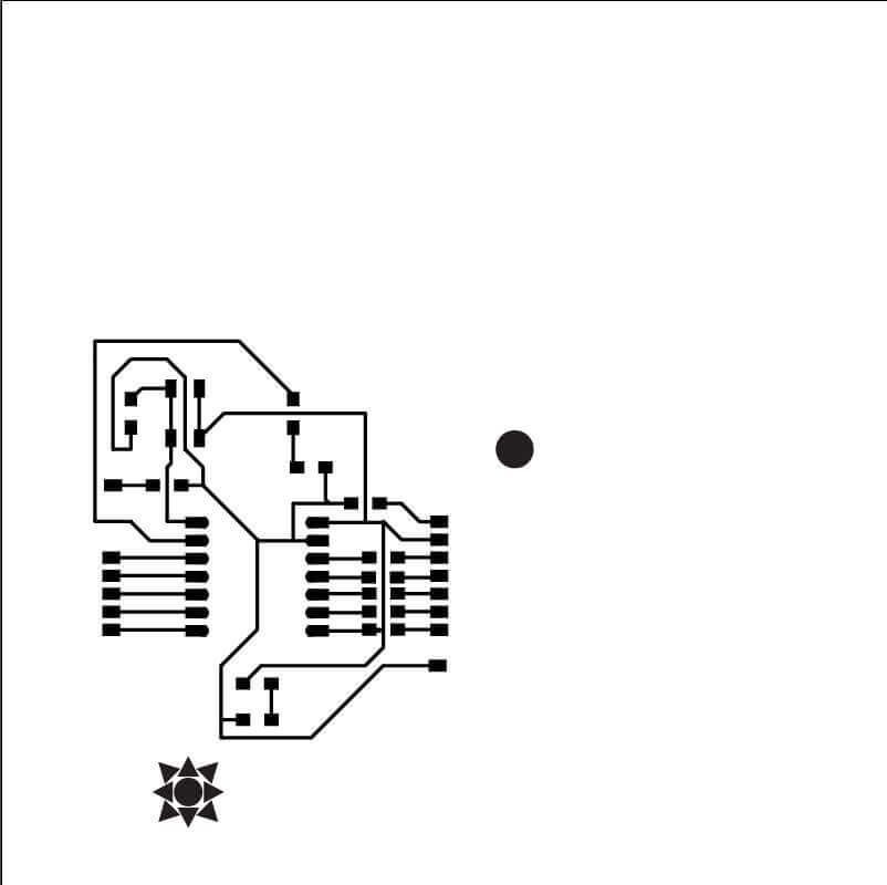
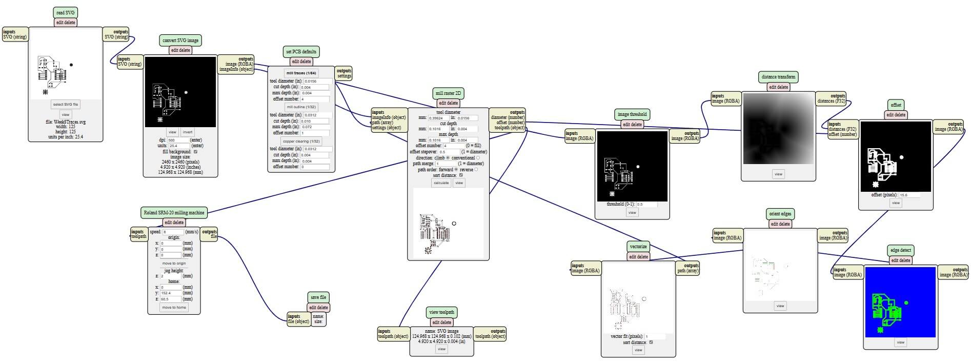
Back in week 6 we had designed multipupose circuit boards to be milled later. This week we built off of those designs and prepared them for milling. We first used adobe illistrate to finalize the board traces, including any decals we wanted to add like my personal logo, and the board outline or shape of the board. We also had to get these two adobe sketches prepared for the MIT mods file converter, a website that helps you convert image files into rml circuit milling files. We did this by setting the images to black and white and seperating the traces from the outline.

Then I went to
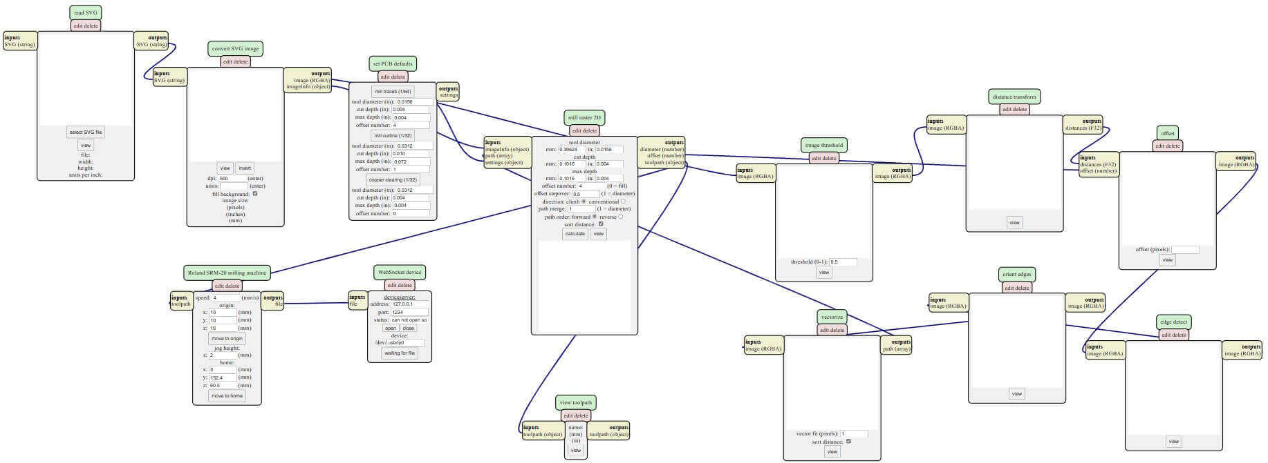
Next, I uploaded the traces svg file to the first function box, you can also start with the outline first, and set the thrid function box to "mill traces" and changed the speed to 10, or 8 for more detailed boards, and zeroed the X, Y, and Z. I then hit calculate and go the calculated traces path.
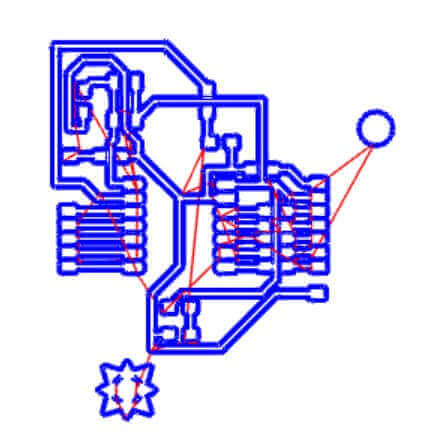
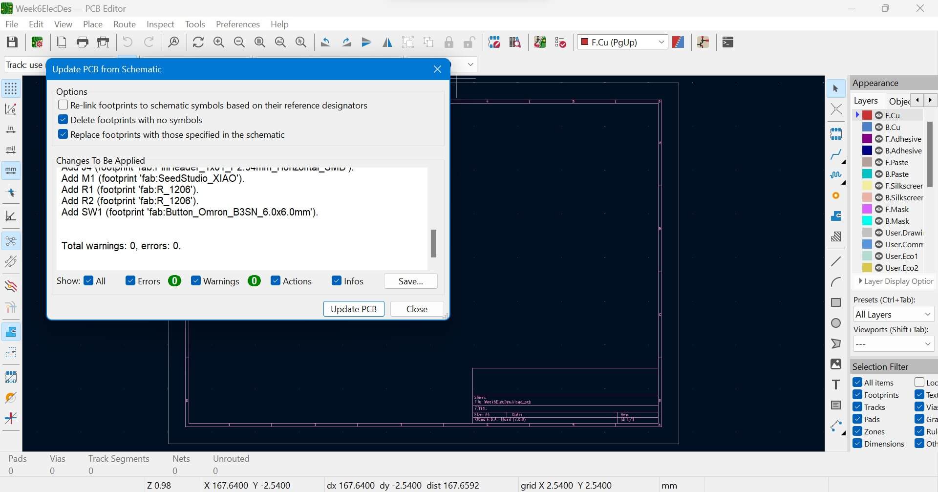
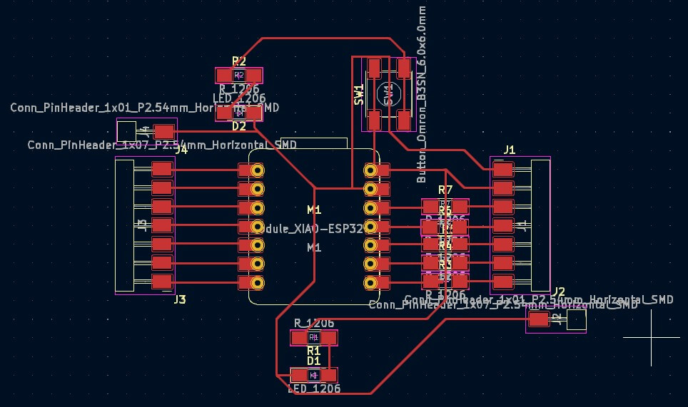
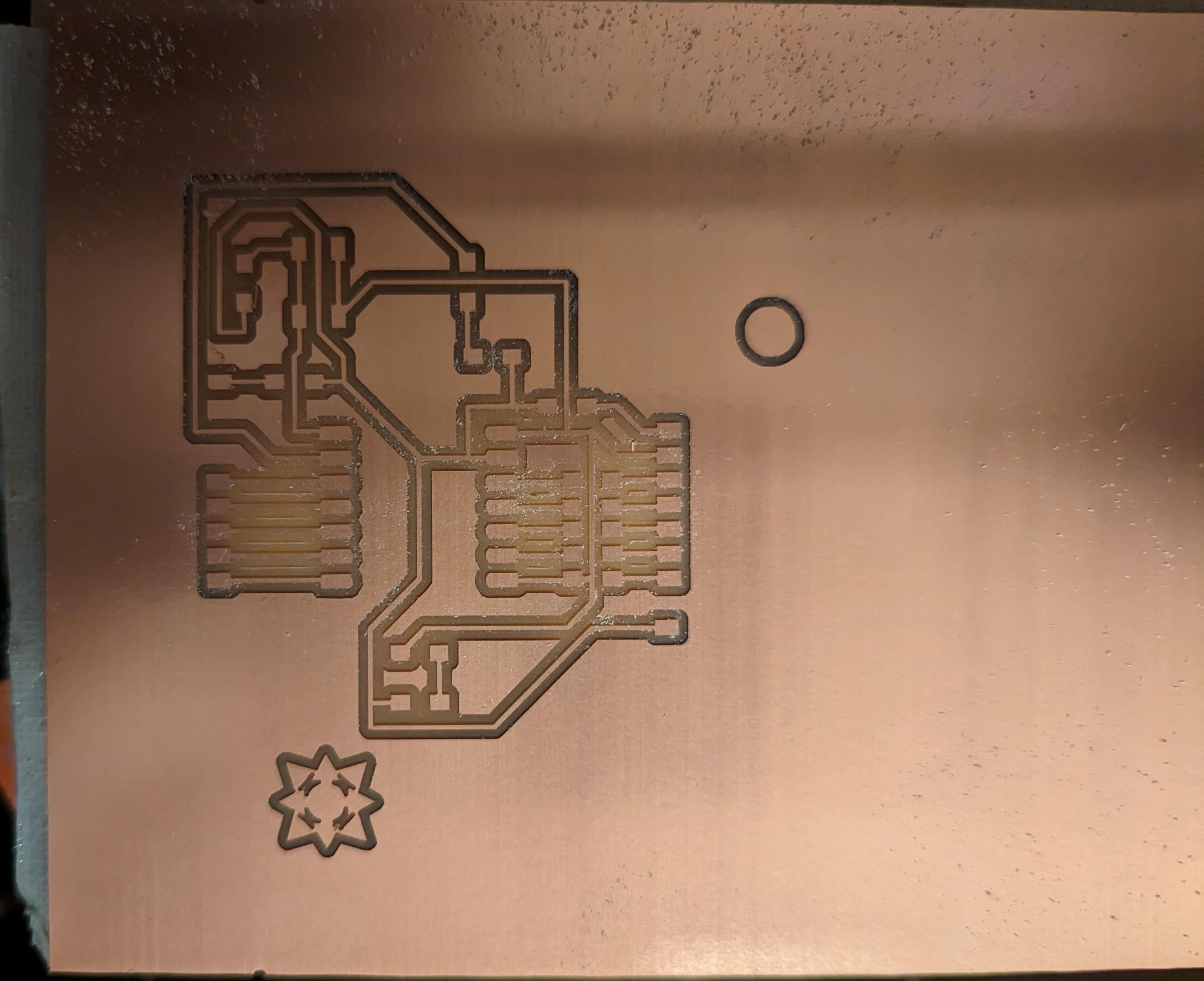
After the skematic was finished and all the "suggestion lines" pointed to the right commponents I started connecting the components. As you can see I used the space under the ESP microcontroller and a few "bridges", 0-Ohm resistors, to make paths that would otherwise conflict with eachother.
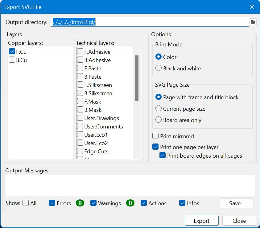
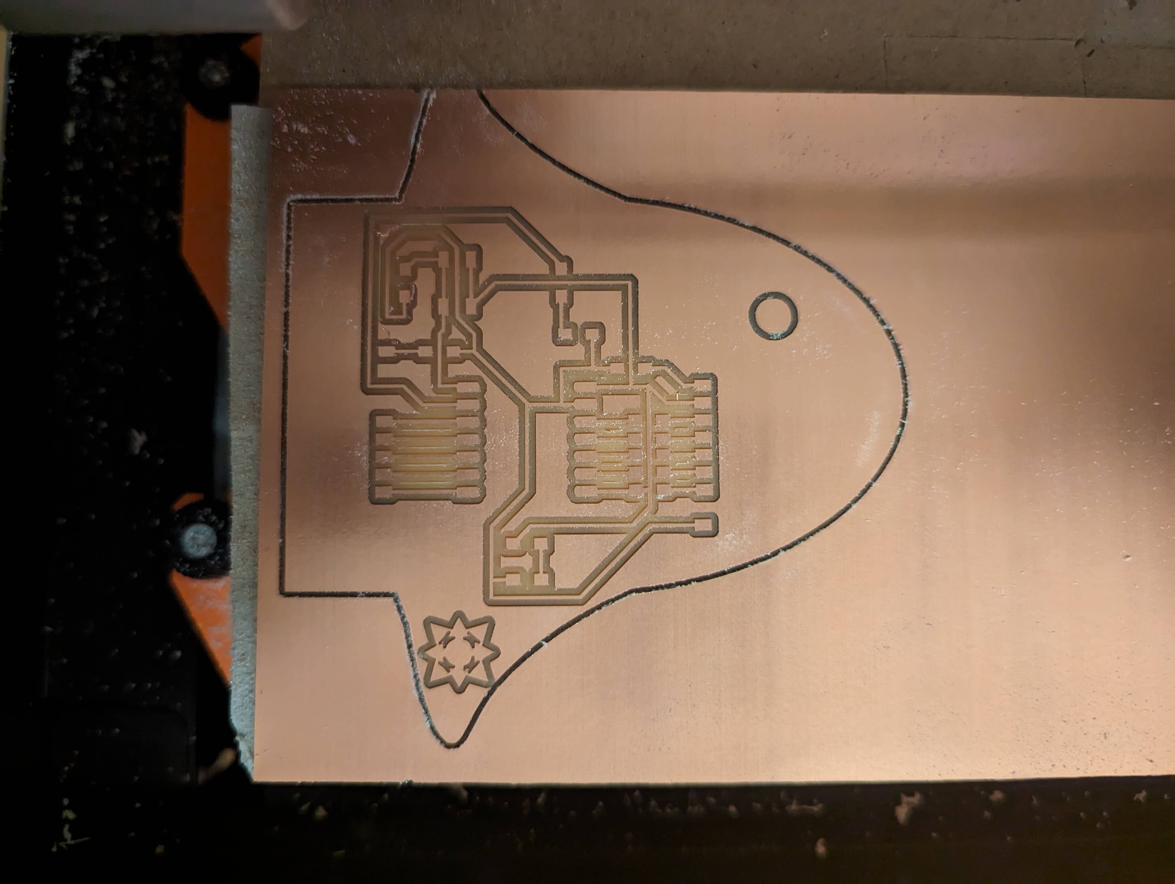
I then exported my PCB blueprint into Adobe Illistrate to create the outer milling cut to create the overall shape and cut it from the board when we mill.
Board Milling
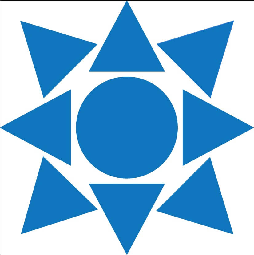
This week I also designed a personal logo I will be putting on all of my projects moving forward. The thought process behind the design is that I have an interest in transportation tecnology. Whether it be on land, in the air, in and on water, or in space, it just facinates me. So I though of symbols or designs that represent travel or transportation, finally resting on a Compass Rose. For the color I just chose my favorate color, sky blue.
Now I was set to send the files to the milling setup we have in the FabLab. Then I took a coppersheet and stuck it onto the coark board in the miller to set it up for cutting.
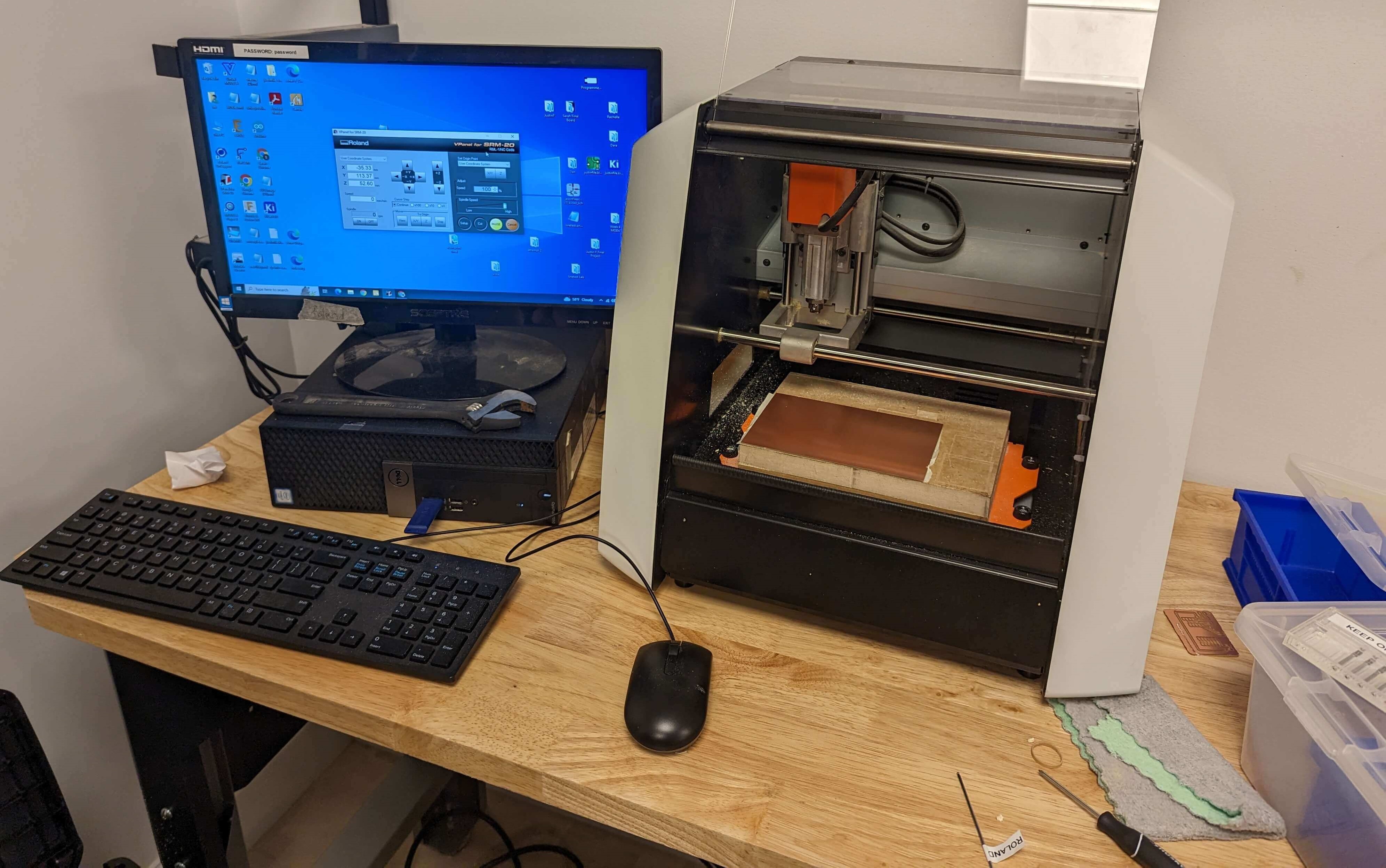
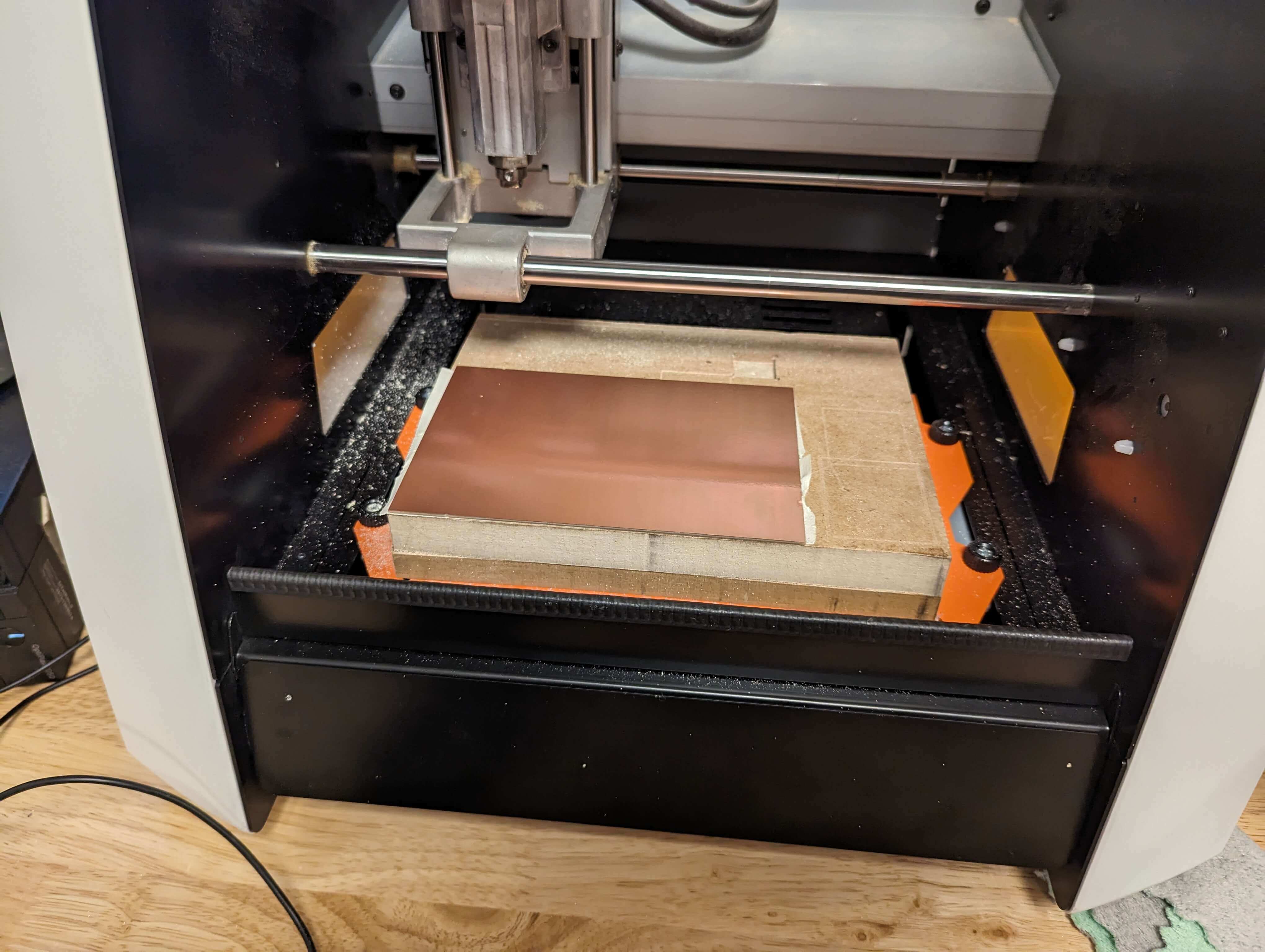
After afixing the correct cutting head to the miller I used the computer next to it to set the 0 point on the board, that being the bottom left, and zeroing the bit to the board. I then set the inner traces file to be milled and let it run while I watch to make sure nothing went wrong. I then set the outer trace to run and once everything was complete I took it off the milling board with a paint scraper.
Lastly I soldered my board with an Esp and all the other components I had planned out in my digital design. This was a very tricky process as most of the compnents and their connections were small and because I wanted to try air soldering with liquid solder. Previously I had taken a circuitry class where near the end we used a stick iron and wire solder. This experience was very helpful in picking the new ways of soldering as well as soldering smaller components.
"Group" Work:
&esmp;Because this week started during spring break we researched and compeleted our projects individually.
Useful links
None for this week.