
Design a development board to interact and communicate with an embedded microcontroller
To design the PCB I used Autodesk Eagle, which is electronic design automation (EDA) software that lets printed circuit board (PCB) designers seamlessly connect schematic diagrams, component placement, PCB routing, and comprehensive library content. Additionally, the name EAGLE is an acronym, which stands for Easily Applicable Graphical Layout Editor.
A schematic diagram is a fundamental two-dimensional circuit representation showing the functionality and connectivity between different electrical components. It is vital for a PCB designer to get familiarized with the schematic symbols that represent the components on a schematic diagram.
Used Components:
Find the limiting resistor value:
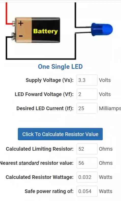
Note: since we got 52 Ohms and we don't have it, I used 100 Ohms.
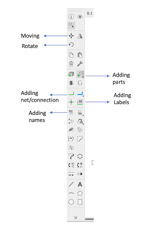
To be able to use Eagle we have to know same important tools in the Toolbar
The following image shows the schematics:
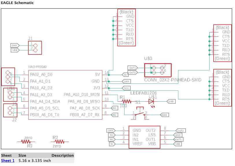
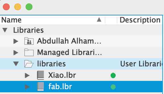
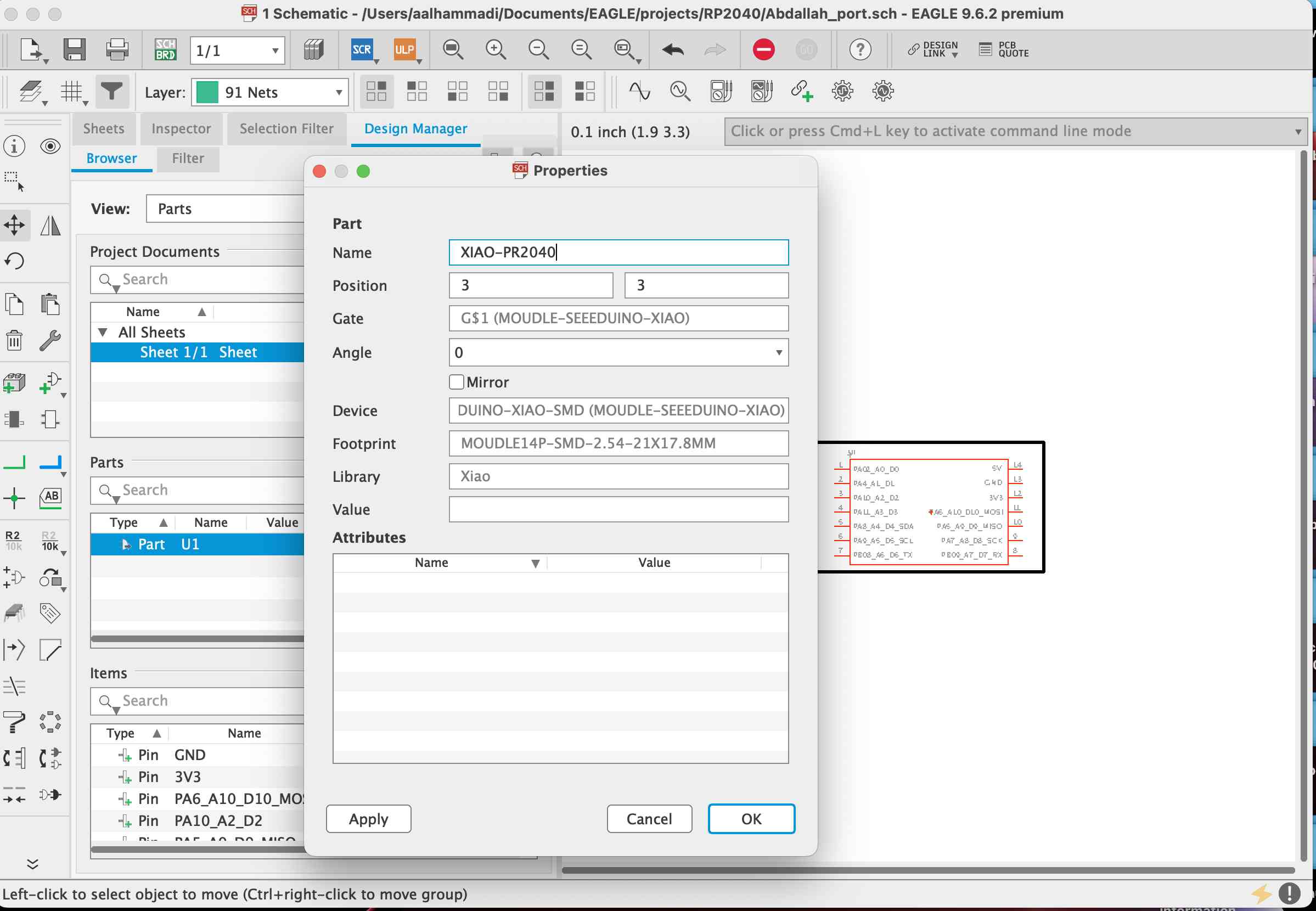
and to add the RP 2040 schematics I use the RP 2040 Eagle Library that we download
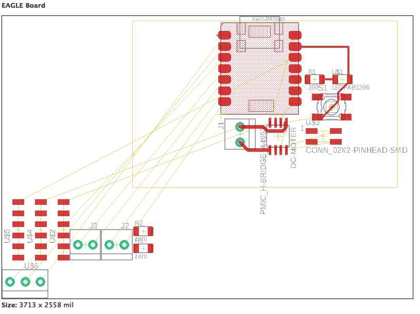
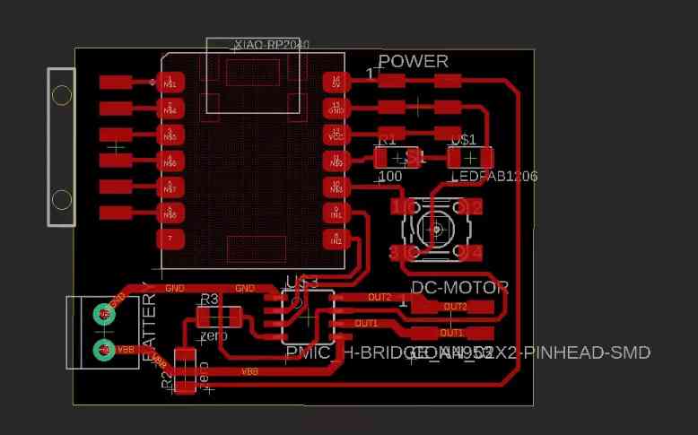
After checking everything are connected in the right place, I converted the Schematic file to the Layout file as shown below:

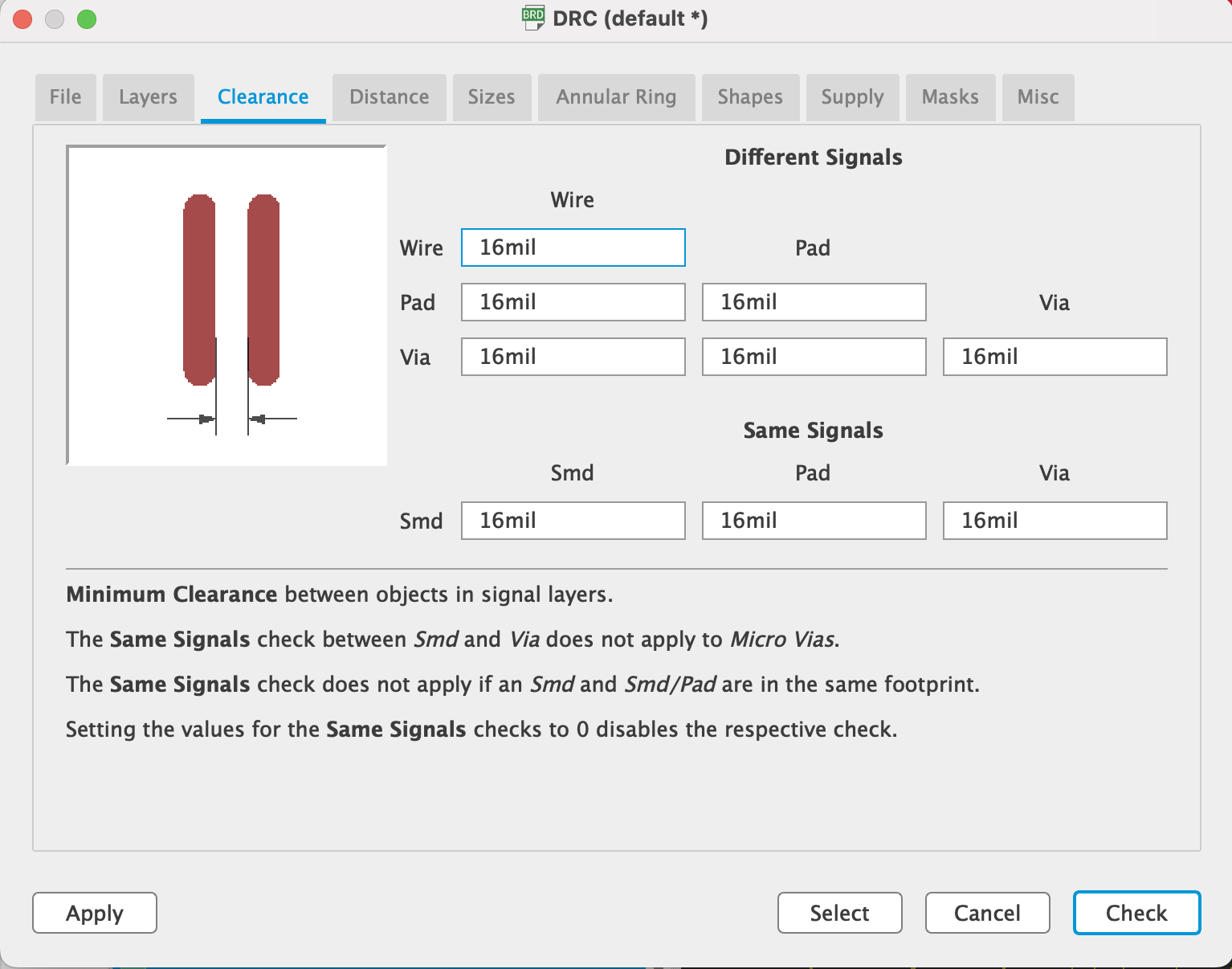
I use the 20 and 18 mil for the clearance routing becuse I use a 0.4mm to cut the profile
Design Rule Checking (DRC): verifies as to whether a specific design meets the constraints imposed by the process technology to be used for its manufacturing. DRC checking is an essential part of the physical design flow and ensures the design meets manufacturing requirements and will not result in a chip failure. The process technology rules are provided by process engineers and/or fabrication facility.
Types of Design Rule Checking:
Each process technology will have its own set of rules. The number of DRC rules and complexity of rules increases as the manufacturing technology shrinks at advanced nodes.
Here are some basic and common types of DRC rules:
The following image shows the Layout:
For the group assignment I will be testing the voltage of the Potentionmeter once we moving it using the multimeter and the oscilloscope respectively,
Multimeter reading
Oscilloscope signals
Multimeter & Oscilloscope