Week 8: Electronics Production
Assignment Activities
1.Group Assignment.
.characterize the design rules for your in-house PCB production process
.extra credit: send a PCB out to a board house
2.Individual Assignment.
.make and test the development board that you designed
.to interact and communicate with an embedded microcontroller.
1.Group Assignment.
characterize the design rules for your in-house PCB production process.
You can access Group Assignment in details here
Individual Assignment.
In this week,was another opportunity for me explore more in electronics,this was really an interesting week because I learnt many things regarding electronics and it's the core thing I wanted to learn in this Fabacademy,though it was tough for me to understand the concept but I have learnt the basics which will help me to deepen my understanding and improve electronic skills as mechanical engineer.
Electronic Production:It basically refers to the process of manufacturing electronic components and devices, such as printed circuit boards (PCBs), semiconductors, sensors, microcontrollers, and other electronic components.
It involves designing the electronic hardware, including components such as integrated circuits, transistors, capacitors, resistors, and sensors, as well as developing software to control the hardware and make it function as intended.
Back in week 6 of electronic design, I designed my PCB with Attiny 45-10SU as my MCU and when we reach the to the interaction between PC and PCB we used Arduino UNO for the communication between the devices means Arduino act as the Programmer, Now in this week I created my programmer which can fit in my PCB.
Below are the steps that I followed in designing,cutting and programming the Programmer.
In designing my Programmer I followed this process;
Firstly was identification of the components to be used in my programmer,the components were:USB Connector,USB to Serial Bus converter chip,oscillator,capacitor,resistor and LEDs.
I do have KICAD Software which is is used to create schematics, printed circuit board (PCB) layouts and also perform simulations
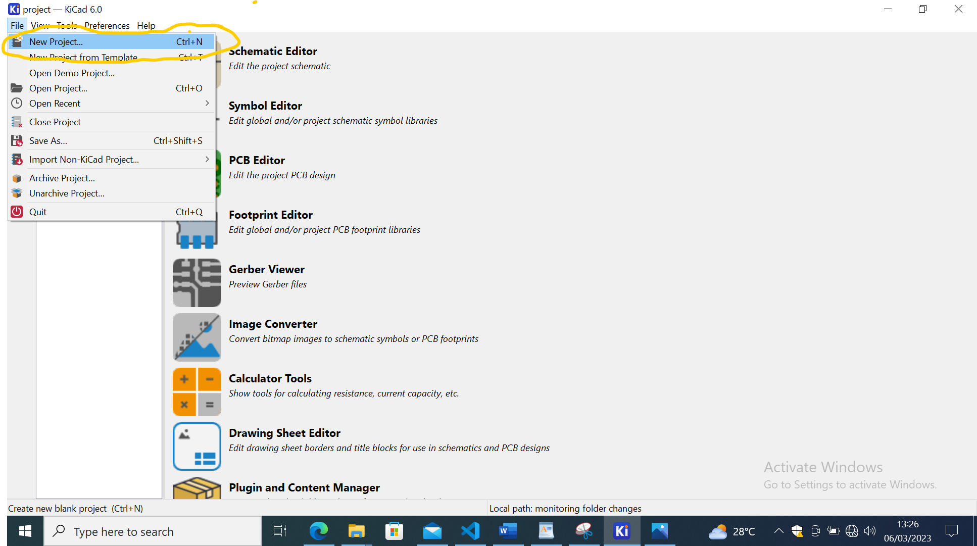
- After identification of the components,I proceeded in creating the new project and saving the file directory and the name, This is the KICAD Interface

- The next thing after creating the project was to insert the components, to add the components in the interface I used tool called"add symbol" after clicking the tool I entered the name of the component they gave me the list of similar components and it was really difficult for me to know the right components to choose(it needs more research to be aware of specifications)(tools added were:Attiny 45V,push button,resistor,LED,connector),and I labeled also push button by using tool called"Label".

- Next step was to connect the components by using wires as we all know electronic device to work needs power so a wire act as the channel for current distribution and I used tool called"add wire".
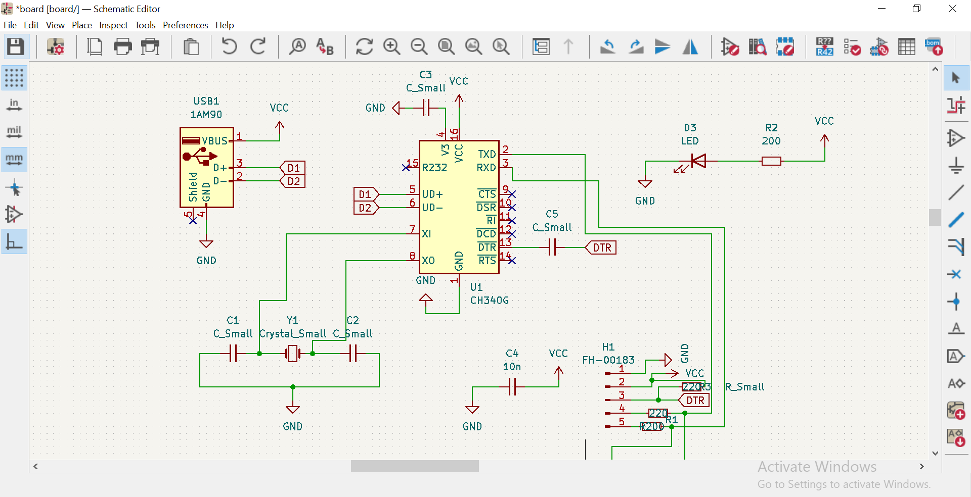
- The next thing is to name the similar components, this is for identification of the components, for instance I have used more 2 LEDs then I was having to identify them like saying LED1 and LED2 to avoid confusing them and this naming is done automatically.

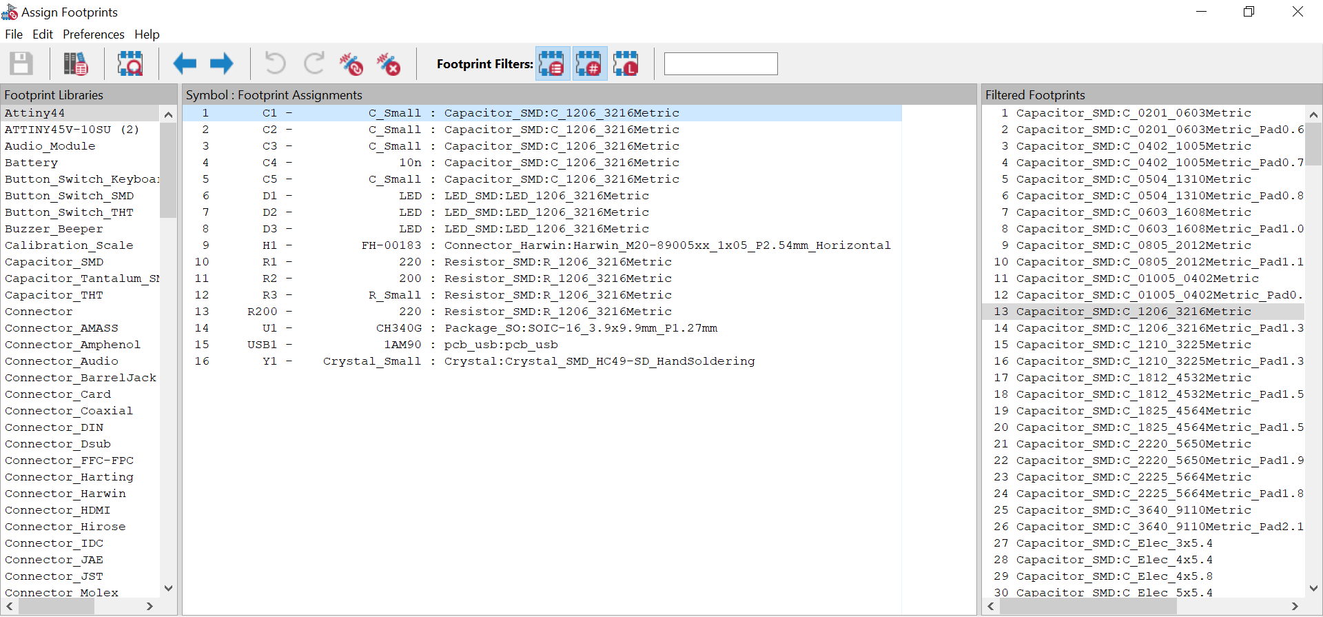
- After annotating the components to assign the components with their specifications,and here I used this icon because there are very many types of connectors and components then I needed to clarify their specifications.

- By clicking the footprint icon,concerning components libraries and their filters,in order to obtain the component's footprint which fits to the ones i used.
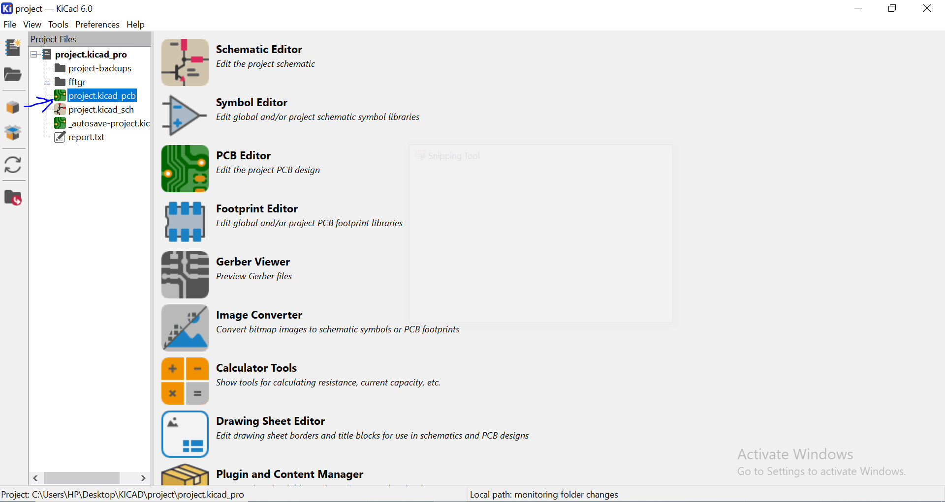
- After Assigning the components,then i went back to starting and click to my project(Kicad.pcb) and then open it for positioning and editing it.
- the time I opened my project in PCB,i edited board and linked all the components with the wires.

- After editing PCB editor,I checked the board in 3D viewer to check how it looks like.

- The next step is to export the designed PCB and save it with an extension of SVG to be used while transform it in readable file.
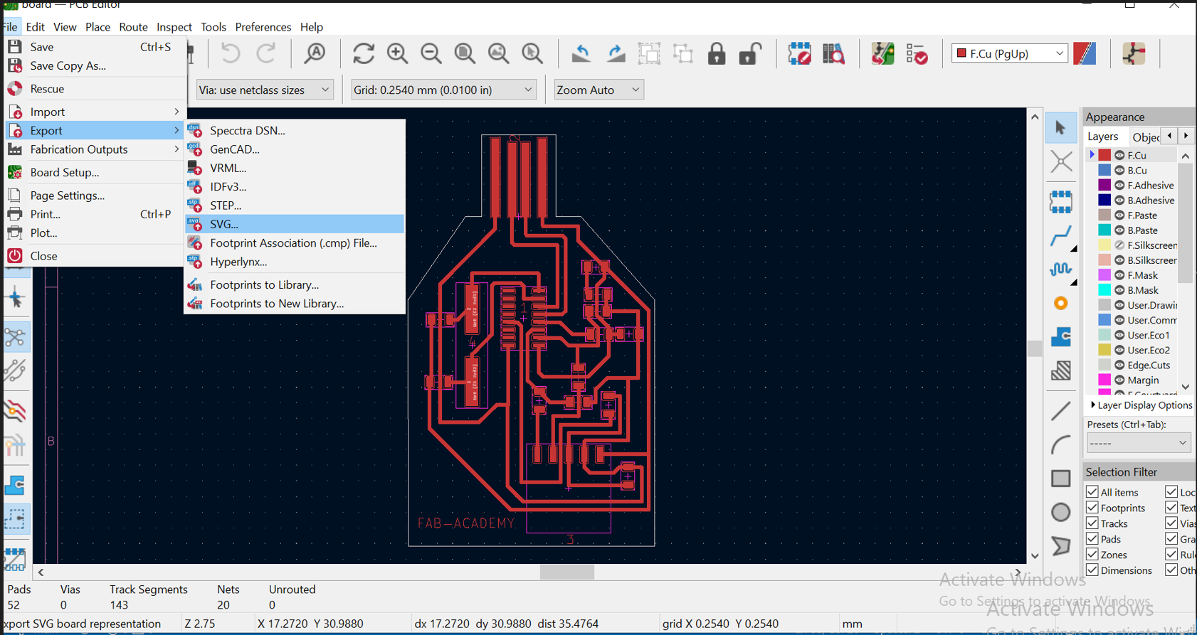
- I changed the properties of the file and change it in black-white and board area only file,and then export to the folder

- After exporting and now I had SVG Files, next is to change my SVG file into Machine readable files(with XRM as extension),below are the steps to change it;
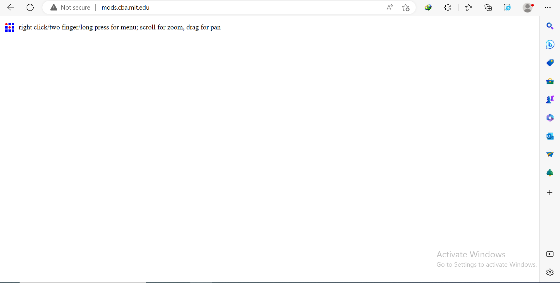
- Firstly,Browse this link here, the site I can access almost all Machines readable files,then after browsing i got this interface.
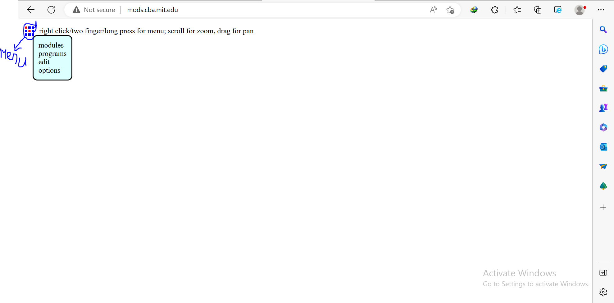
- Then I go to this menu and right click where there are options, as stated above.
- next I clicked on the programs,next click on open server, next is Roland because it is our machine in our node and click on the SVG file since it was my extension.
- the next after clicking on SVG File, the displayed interface was this.

- and the remaining thing is to select the exported file and put it there to be changed.
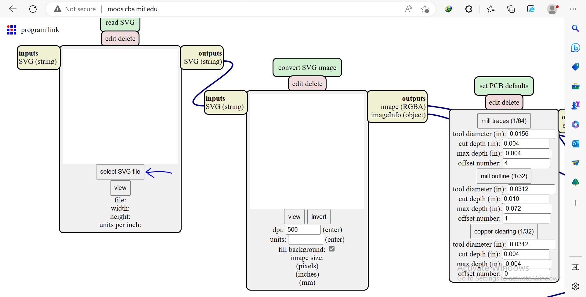
- after clicking on select file, exactly I go where my file was and click open.
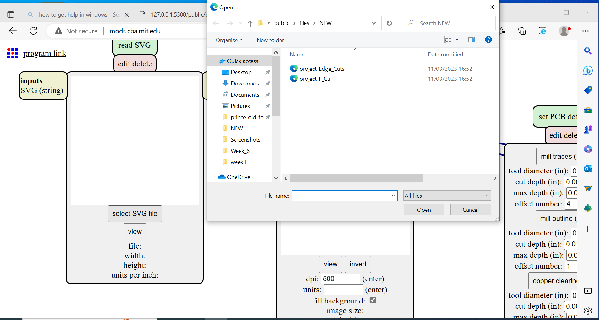
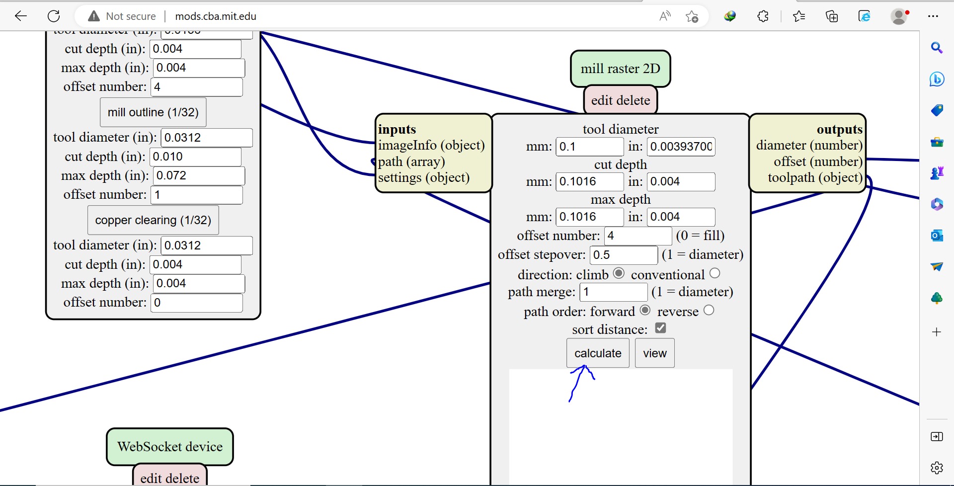
- Then we change the settings after inserting the file, we first invert the image and change dpi to 1000 so that our machine could cut it and the ways can be visible.

- because i first having to trace the way which looks similar to engrave in laser machine, then i selected mill trace in order machine to engrave the way, and to cut the pcb frame I used another file and I used mill outline.
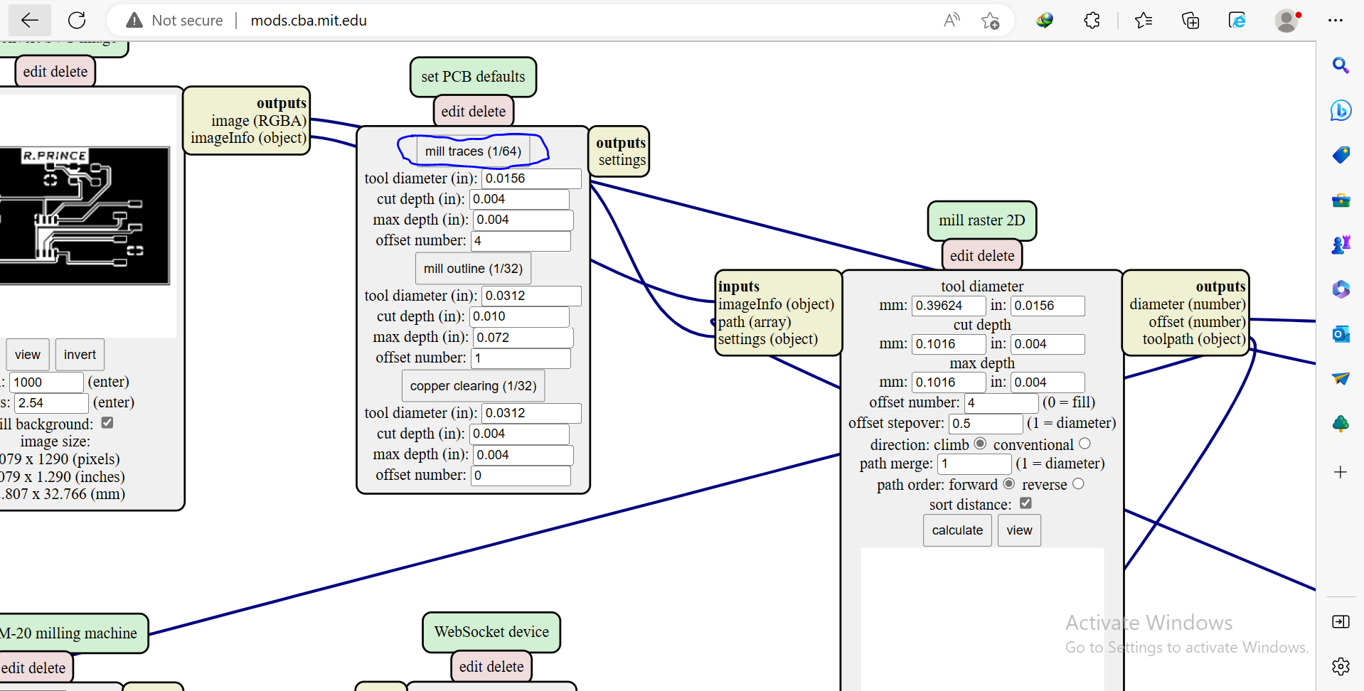
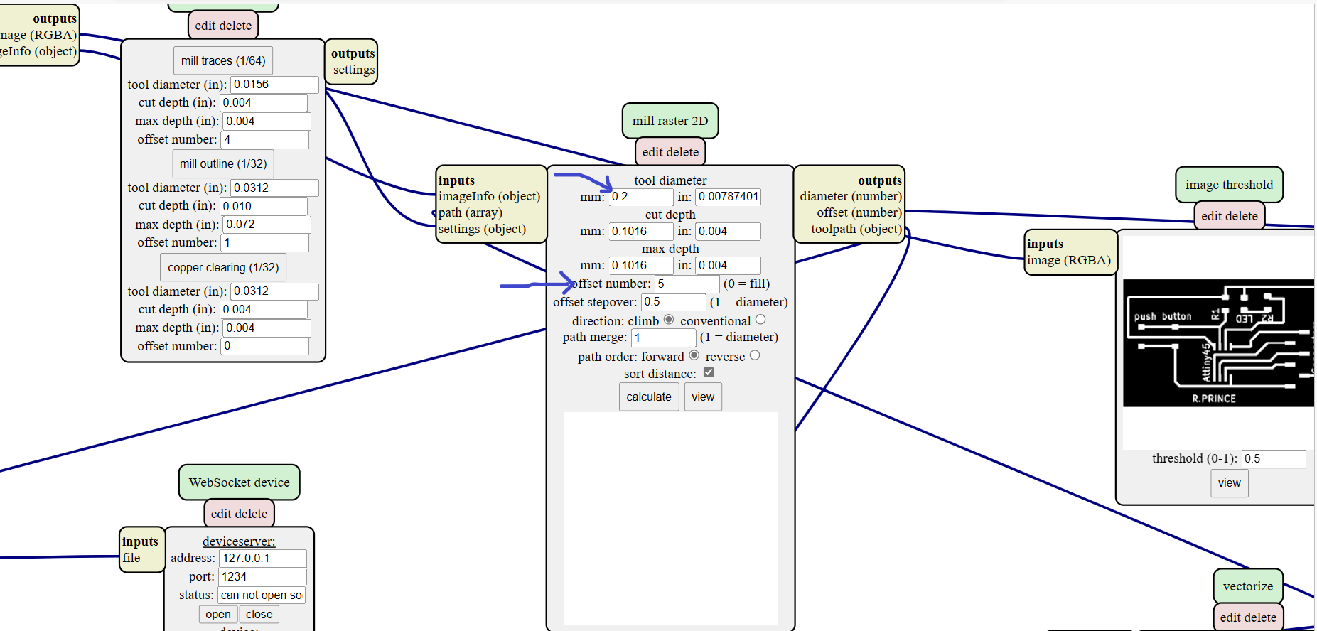
- Then because of the tool to be used after measuring I got that it's diameter of 0.2 mm,and I also setted offset(5) means it passes 5 times and my way will be enough to solder,then it's the one I added.
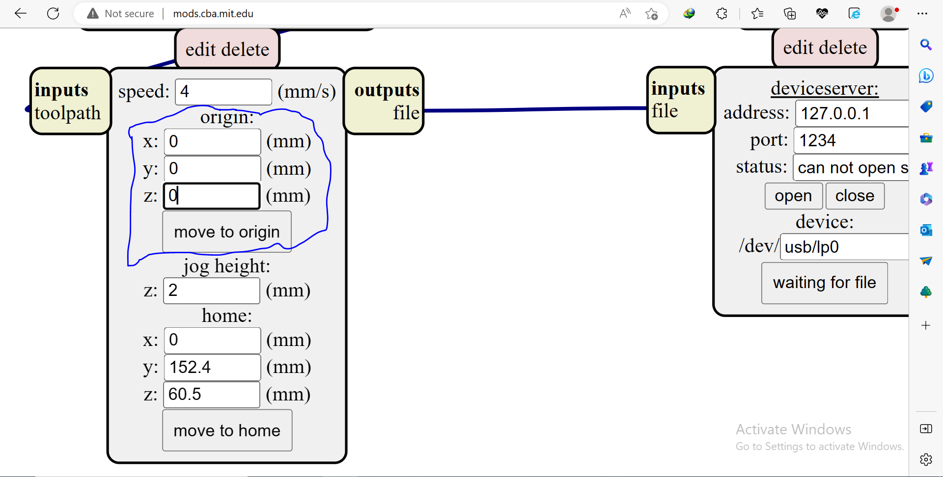
- Next thing is to change the origin or starting point of the machine,by changing and starting point be(0,0,0)
- Then add the input and output channel where I will immediately save changed save in my computer, means it will be downloaded, then I right clicked and go to the modules, open server and select save(file) then it will be displayed.
- Then after I have to link output and input by dragging the cursor to create a connection.

- Then click button calculate under mill raster 2D table
- Then automatically the file to be send to the machine will be downloaded and tool path while milling.
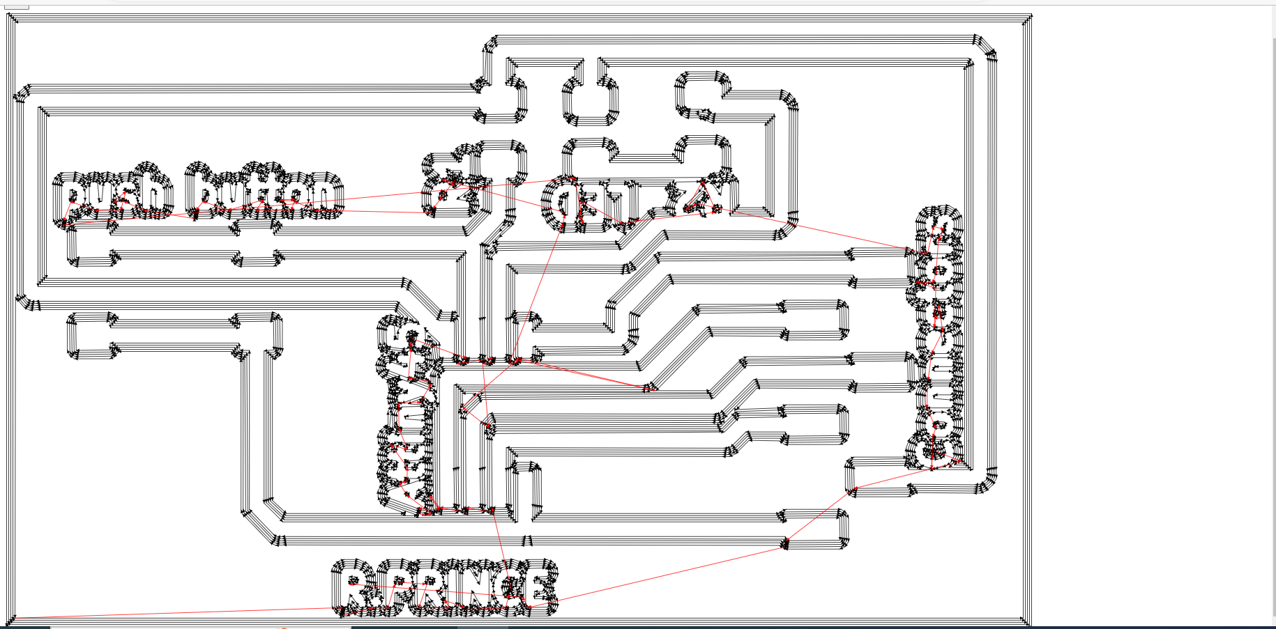
Tool Path
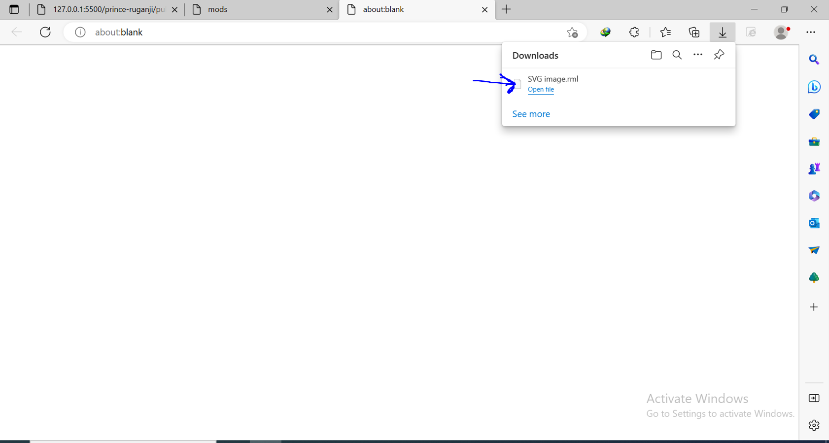
- The final output of the my PCB to cut ways.

- The final output of the my PCB to cut PCB(edge cut).
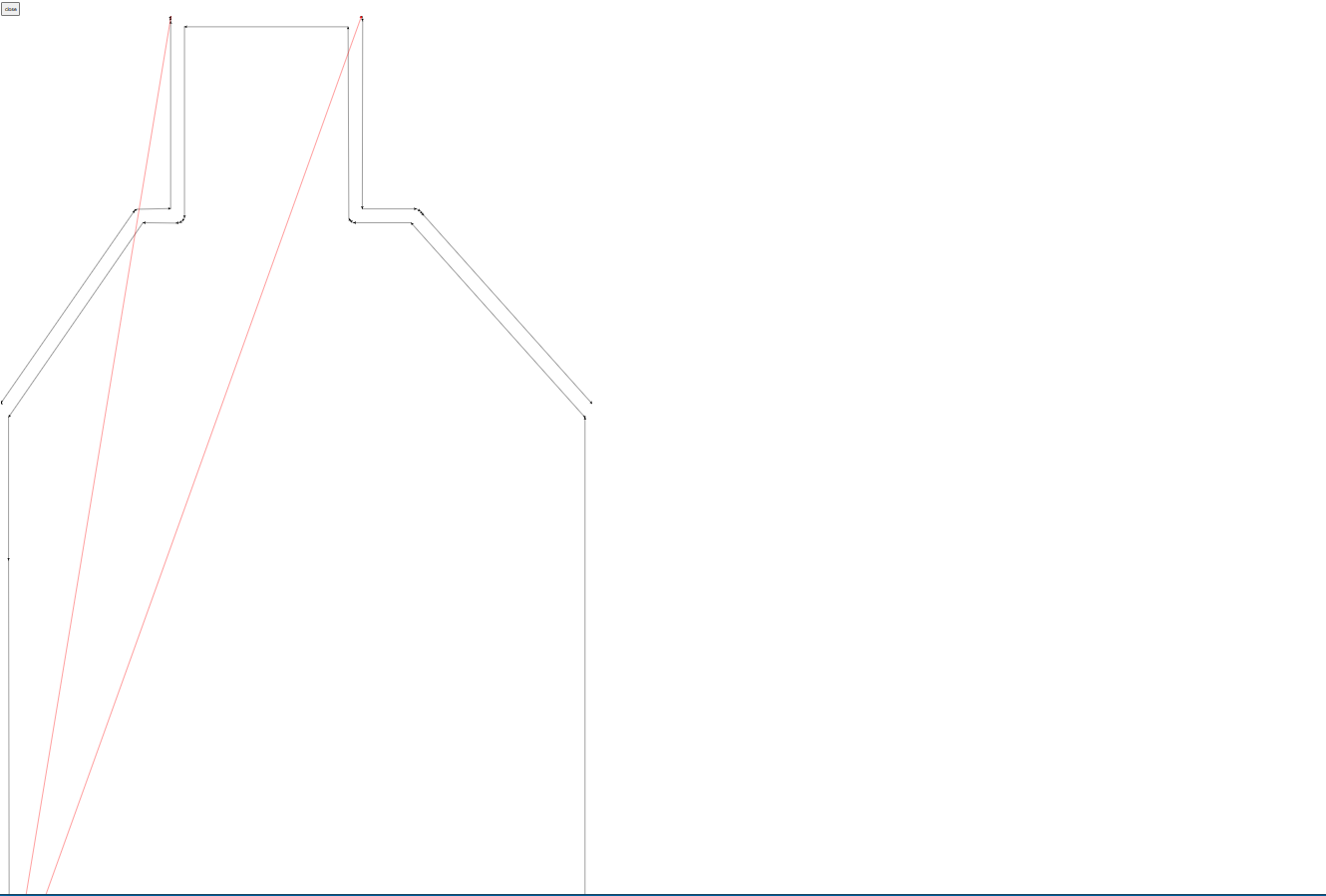
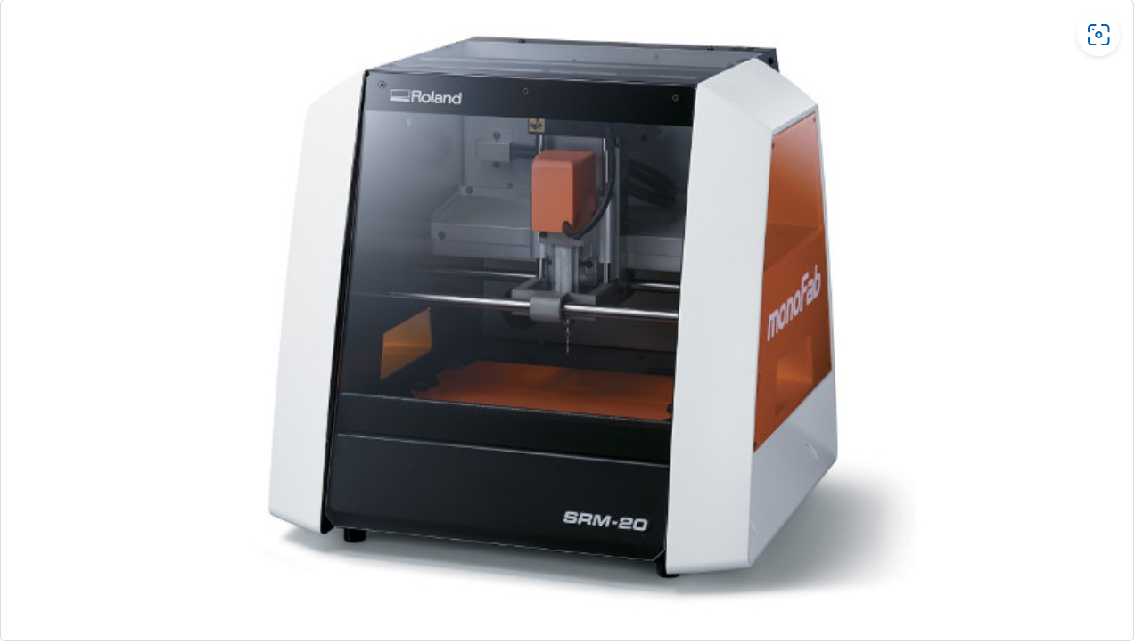
- The next after changing the extension of the file remaining is to go to the milling machine,and I started
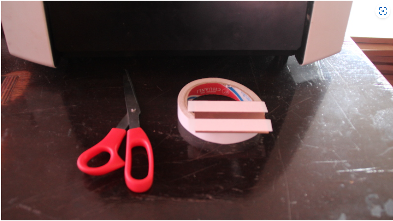
- Now I taped on the back of the PCB and I using FR4 board(One sided).
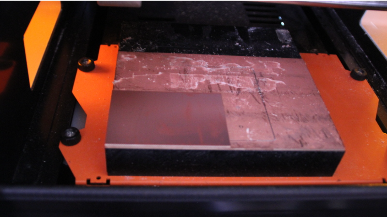
- Now I have already fixed the board on the bed, I am ready to setup the machine and start milling.
- Then I was having to set the origin of where it will start in cutting ways, I used the software called "Vpanel" for SRM-20 in controlling the position of tool.

- then after setting the tool position,It starts cutting the board.
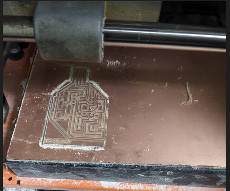
- The final output after cutting my PCB.
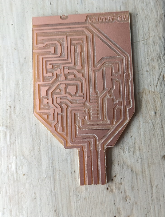
- the components i used in my programmer.

- Then after identification of the components for the my Programmer, I proceeded with soldering below is the picture after soldering all components on my board.

- Then after soldering my programmer,I proceeded with checking of my programmer if it really works, I needed to install the drivers of USB to Serial Bus converter chip(CH 340G),below are the steps I took to install it.
- I first go to google search"CH 340G drivers",or you use this link to install the drivers for windows 10/11,below is the interface where I reached and click on button download.

- then after downloading setup after I was reamining to install it, for the prompt(using read me) and click on button install,and it will be installed successfully.
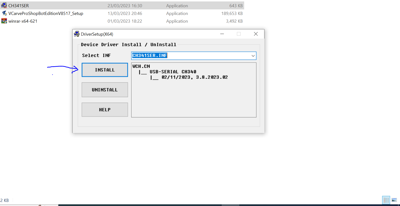
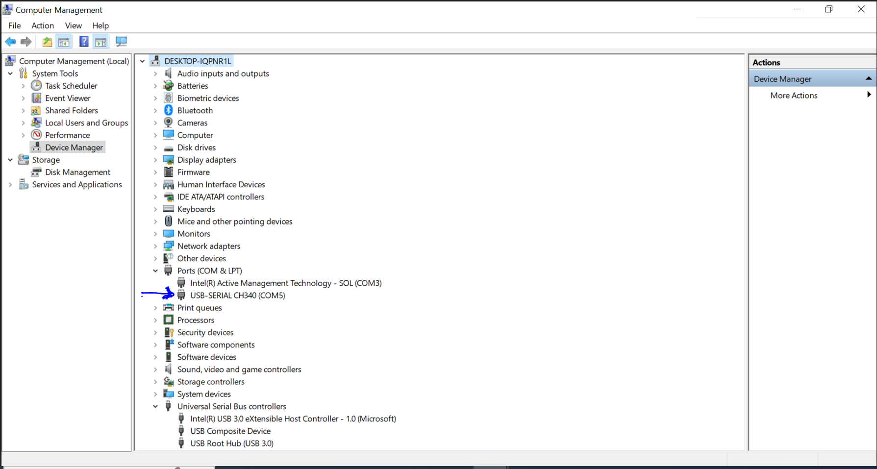
- Then after the installation of the chip driver(CH 340G), I connected the Programmer and checked if it was recognised.
- Once I plugged in the board in the my USB Port power LED starts to blink and I heard the sound in my PC detecting external device plugged,
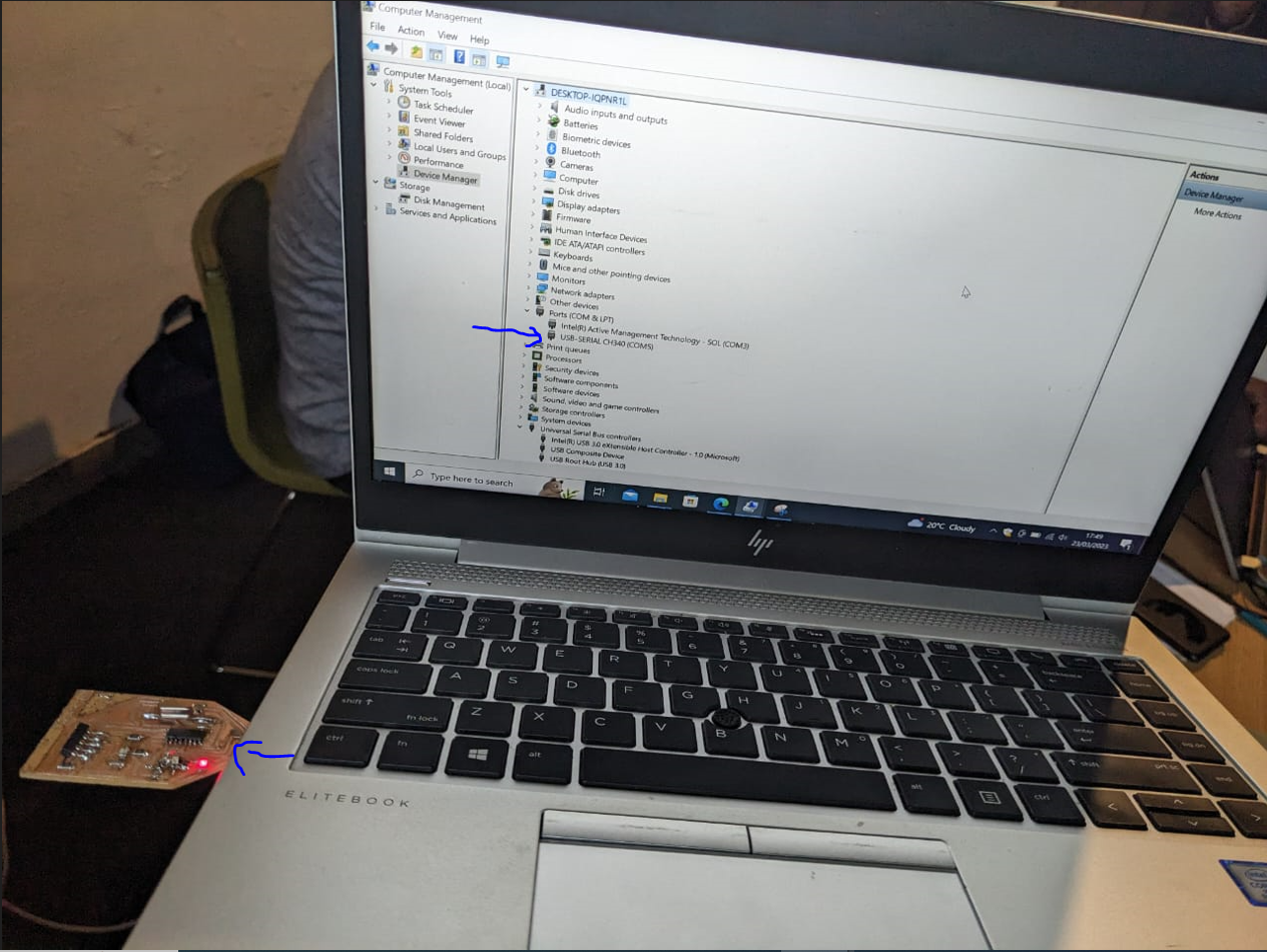
- Then to check if it is recognised in my port, I opened window explorer or press start button and letter E, and press right click and click on manage.
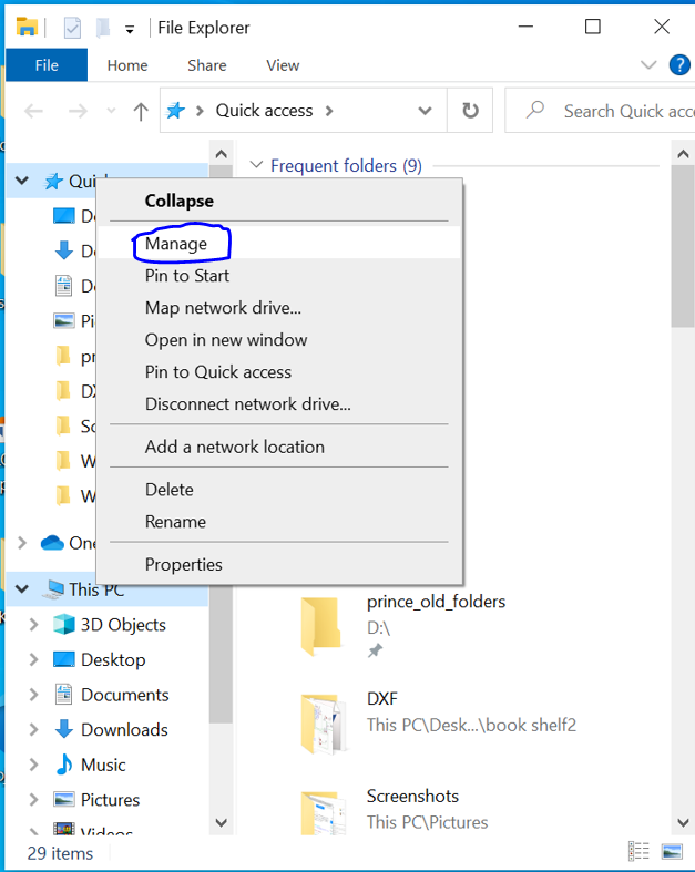
- I checked it and definately found it recognised.
As summing up I can say in this week I learnt more,but major thing I have realised Working with machines requires a variety of skills,knowledge and mostly it's to work with more attention to PCB because any slight mistake can damage the whole work you have done, I have seen it while soldering and cause some short circuits which became more difficult to debug.
hereyou can download the files.
