Eletronics Design
Assignment
more detail will shown on class link
IN our lab the instructor explains the major fator to consider When designing for pcb board, there are some design rules that you should keep in mind to ensure successful pcb board. Here we got some key tips to help you test the design rules for pcb design
here there is more description on work on this group web page:Group work can be found hereIndividual assignment
DESIGN PROCEDURE OF MY DESIGN of my development board
Introduction
In this week of eltronics design i followed my professor guidenceto read the book callled art of eltronics by PAUL HOROWITZ WINFIELD HILL. here i read the background of elotronic where the foundermental issues to review before you dive in eltronics is to understand the current, voltage and resistance and other eletrical accesories like diodes and capacitor even transistor bellow you can find the summary of the eltronics design
- Voltage and current
There are two quantities that we like to keep track of in
electronic circuits: voltage and current. These are usually
changing with time; otherwise nothing interesting is happening.
Voltage (symbol V or sometimes E). Officially, the voltage between two points is the cost in energy (work done) required to move a unit of positive charge from the more negative point (lower potential) to the more positive point (higher potential). Equivalently, it is the energy released when a unit charge moves “downhill” from the higher potential to the lower. Voltage is also called potential difference or electromotive force (EMF). - Current (symbol I). Current is the rate of flow of electric charge past a point. The unit of measure is the ampere, or amp, with currents usually expressed in amperes (A), milliamperes (1 mA = 10−3 A), microamperes (1 μA = 10−6 A), nanoamperes (1 nA = 10−9 A), or occasionally picoamperes (1 pA = 10−12 A). A current of 1 amp equals a flow of 1 coulomb of charge per second. By convention, current in a circuit is considered to flow from a more positive point to a more negative point, even though the actual electron flow is in the opposite direction.
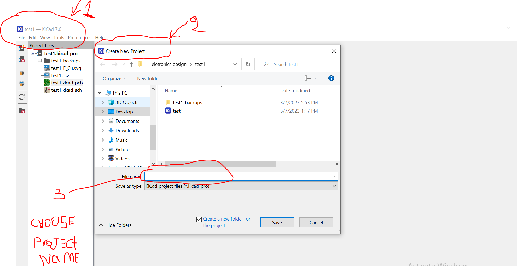
installation of kicard
the procedure used of installing the kicard a popular open-source electronics design automation (EDA) software,are listed bellow
- Go to the official KiCad website at https://www.kicad.org/download/windows/ and download the appropriate version of KiCad for your operating system (Windows, Linux, or macOS).
- Once the download is complete, run the installer file and follow the on-screen instructions to install KiCad on your computer. During the installation process, you may be prompted to choose which components of KiCad to install, such as libraries, demos, or documentation.
- After the installation is complete, open KiCad from the Start menu (on Windows) or from the Applications folder (on macOS). If you're using Linux, you can launch KiCad from the terminal by typing "kicad" and pressing Enter.
- When you first launch KiCad, you may be prompted to configure some settings, such as the default schematic and PCB templates or the location of your project files. You can choose the options that best suit your needs or leave the defaults unchanged.
- You're now ready to start using KiCad! You can create new projects, design schematics and PCB layouts, and export your designs in various formats. To learn more about how to use KiCad, you can check out the official documentation, online tutorials, or forums.
Design of develpment bord to interation and communication with embended microcontroller
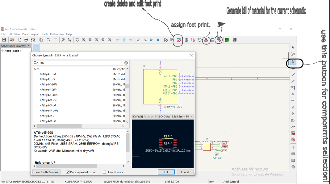
The first step i used in creating a development board in KiCAD is to start with a schematic. This involves creating a visual representation of your circuit, including all of the components that will be used and how they are connected. To do this, i use KiCAD's schematic editor, which allows you to place components, connect them with wires, and label the connections with net names.

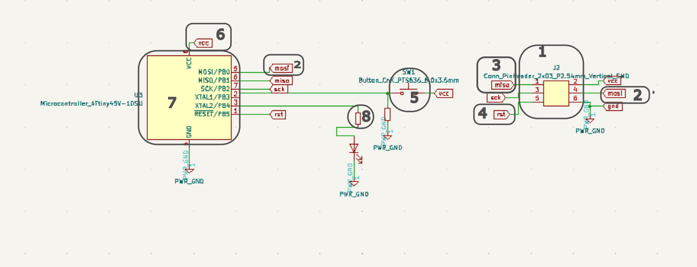
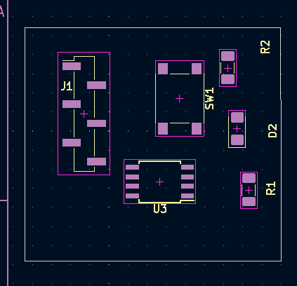
SCHEMATIC DIAGRAM COMPONENTS DESCRIPTION
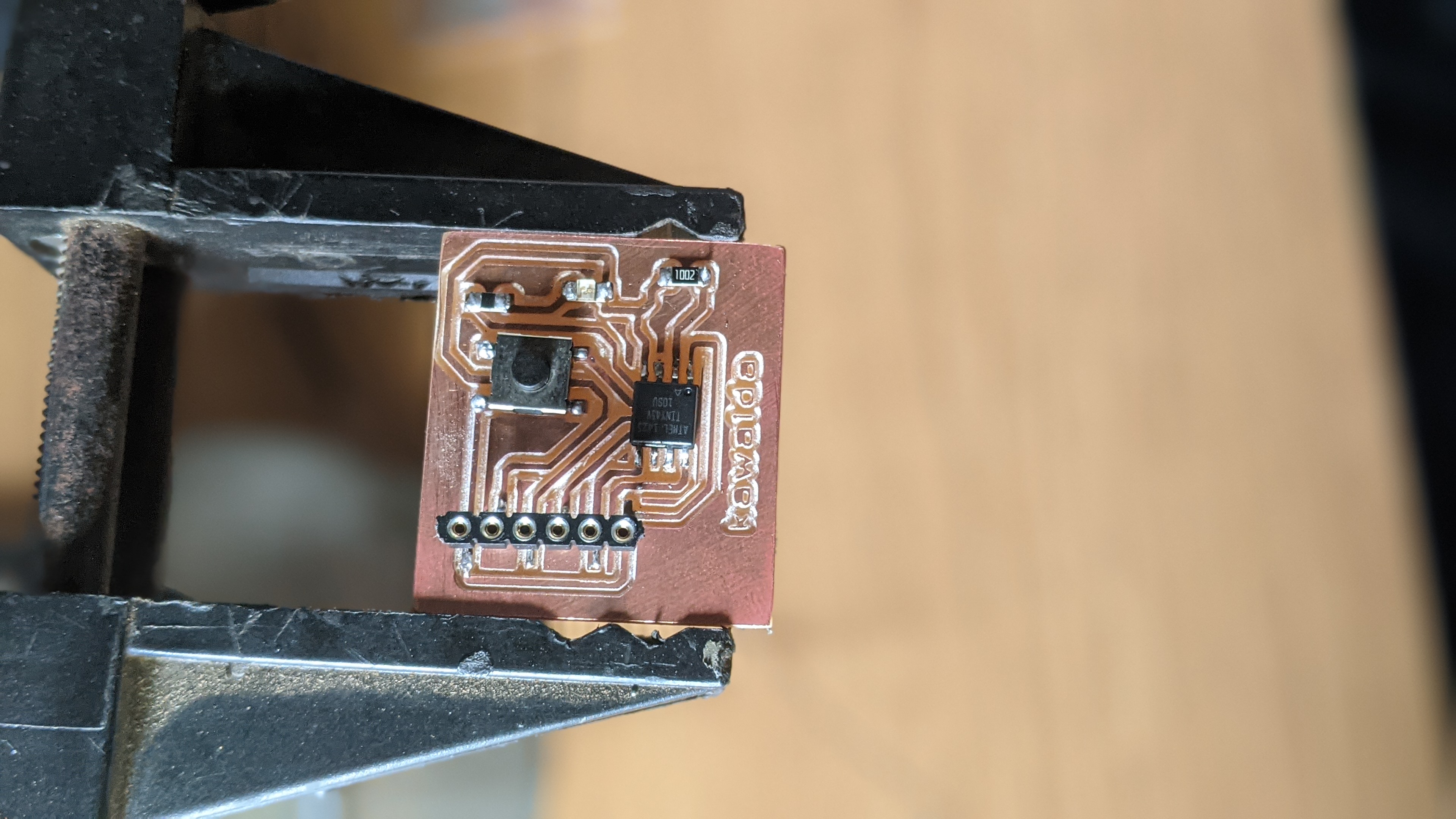
- we used this A pin header in order to get access on mcu pins for the purpose to transfering the code and command to actuate the led on our development booard A pin header is an electronic component that is typically used to connect one circuit board to another or to an external device. It consists of a row of metal pins, which are designed to fit into a corresponding socket or connector on the other board or device.
-
number (2),(3),(4), refer to the one of global lables used with explanation labels are explained below
MASI (Master Out Slave In) and MISO (Master In Slave Out) are both global labels used to
represent the data transfer lines in a SPI (Serial Peripheral Interface) communication protocol.
In SPI communication, there are typically at least two devices involved - a master and a slave. The master device controls the data transfer and sends data to the slave device via the MASI line, while receiving data from the slave device via the MISO line. In KiCad, global labels are used to assign a specific name to a net (a collection of connected wires or pads) that is used throughout the schematic or PCB layout. By assigning the names MASI and MISO to the appropriate nets in your design, you can ensure that the software knows which nets are being used for SPI communication, and can generate accurate netlists and other design files. - we used Push-button switches called the PTS636-60x3.6mm are commonly used in electronic circuits as momentary switches for user input or control. They can be used for a variety of applications,
- in our lab we decide to use The ATTINY45V-10SU
which is a type of microcontroller manufactured by Atmel Corporation
(now owned by Microchip Technology Inc.). It is part of the AVR family of microcontrollers
and is a low-power,
high-performance device with advanced RISC architecture.
The ATTINY45V-10SU has 4 kilobytes of flash memory for program storage, 256 bytes of SRAM for data storage, and 128 bytes of EEPROM for non-volatile data storage. It also has a 10-bit ADC (analog-to-digital converter), 5 channels of PWM (pulse-width modulation) output, and multiple communication interfaces including SPI (Serial Peripheral Interface) and I2C (Inter-Integrated Circuit) protocols.
.The ATTINY45V-10SU is available in a small surface-mount package and is well-suited for a variety of applications including sensors, motor control, lighting control, and consumer electronics. Its small size, low power consumption, and advanced features make it a popular choice for embedded systems and IoT (Internet of Things) devices.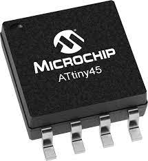
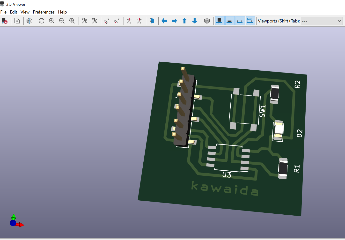
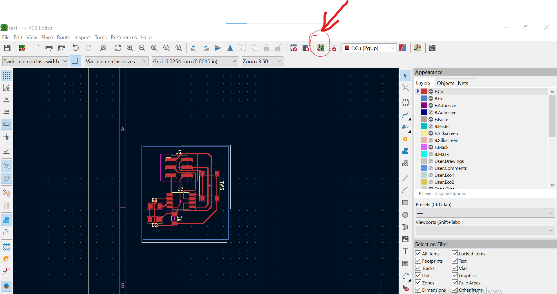
PCB BOARD DESIGN AND DEVELOPMENTS
in order To switch from the schematic diagram to the PCB layout mode in KiCad, we need to first ensure that the schematic is complete and all components are connected properly. Then, click on the "PCB Layout Editor" icon in the main toolbar, or use the hotkey "Ctrl+P" to switch to the PCB layout mode. Once you do this, the software will automatically create a new blank PCB layout file for the current project.

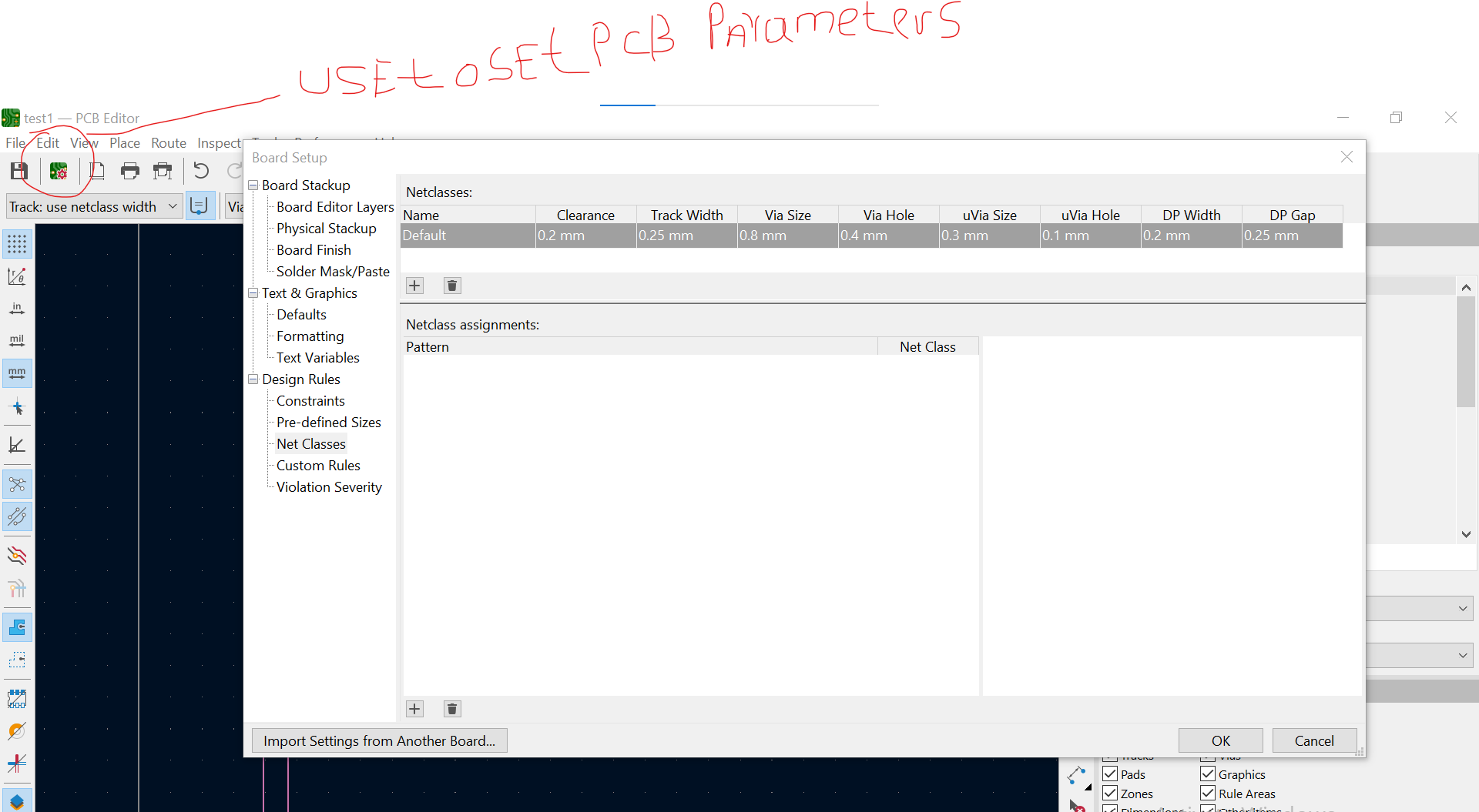
PCB DESING RULE USED
- To set the track width and clearance in KiCad, you can open the "Design Rules" dialog box by clicking on the "Tools" menu and selecting "Design Rules." In the "Design Rules" dialog, you can specify various design parameters, such as minimum and maximum track width, clearance, and via size. You can also set different rules for specific nets or layers. Once you have entered the desired values, click "OK" to save the settings.
- To apply the design rules to your PCB layout, you can click on the "Update PCB" button in the "Design Rules" dialog box. This will apply the rules to your existing layout or any new layout you create.
- Additionally, you can also set other design parameters such as pad sizes, drill sizes, copper pour settings, and more in KiCad. These settings can be found in the "Footprint Editor" and "PCB Layout Editor" menus. By customizing these settings to fit your specific requirements, you can ensure that your PCB design meets the necessary specifications and functions correctly.
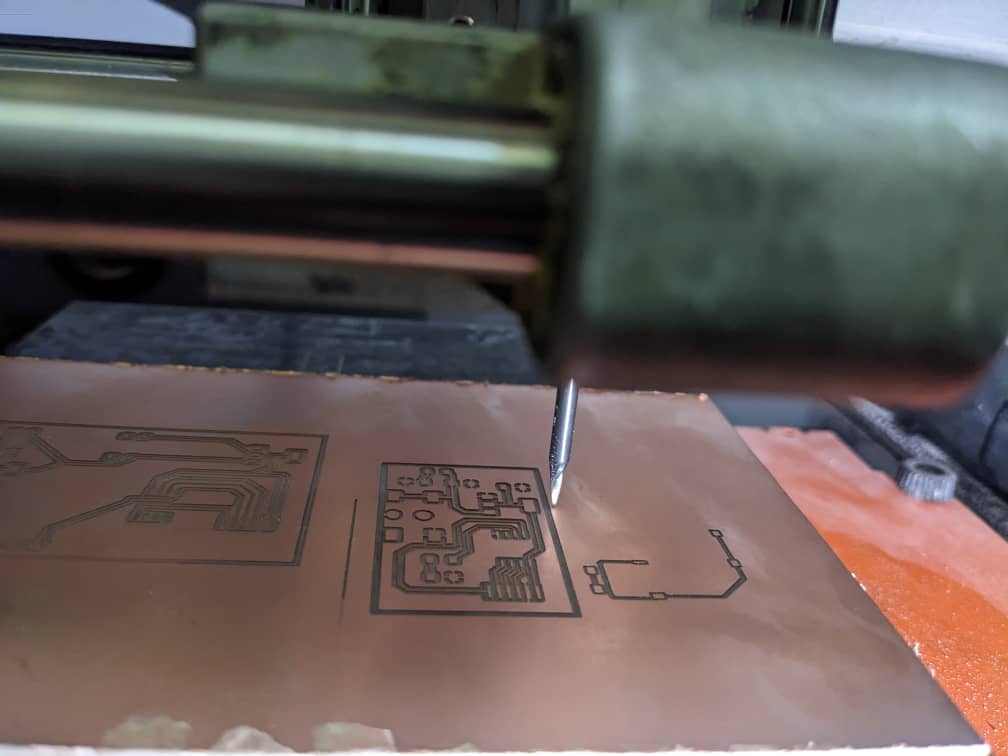
- Open your web browser and go tohttps://mods.cba.mit.edu/. This is the website for the Massachusetts Institute of Technology (MIT) Center for Bits and Atoms (CBA) Modular Machines program.
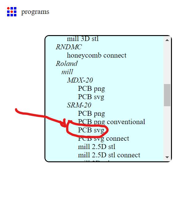
- Click on the "Mods" button on the top right corner of the screen, and then select "Roland" from the drop-down menu. Roland is a type of milling machine that uses G-code to operate.
- Once you've selected Roland , you'll be taken to the Roland module page. Click on the "Open Roland " button to open the Roland software.
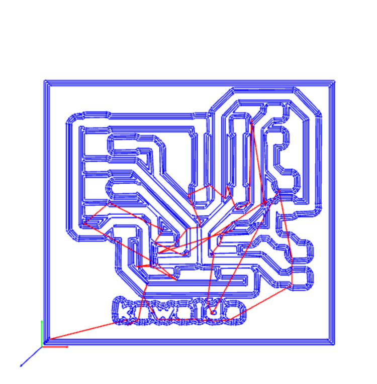
- In the Roland software, click on the "File" menu and select "Import." Choose your SVG file from your computer and click "Open." Your SVG file will now be loaded into the Roland software.
- after satisfied with my settings, click on the "Post" button to generate the G-code for your milling job. The G-code will be displayed in a new window.
- Copy the G-code and save it as a text file on your computer.
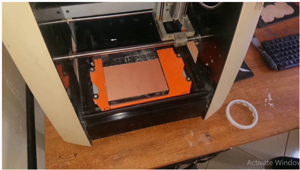
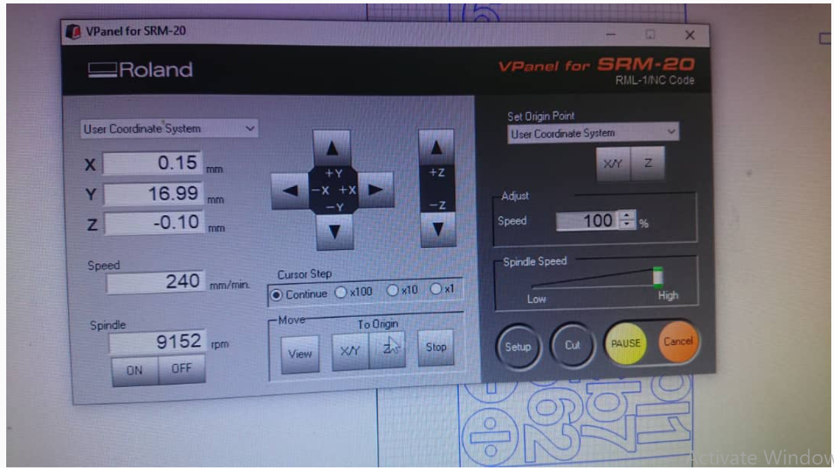
- Connect your Roland SRM-20 milling machine to your computer using a USB cable.and set the pcb work piece.
- Open the Roland SRM-20 software and click on the "File" menu. Select "Open" and choose the G-code file you just saved.
- Click on the "Send" button to send the G-code to your milling machine. The Roland SRM-20 will now start milling your design.
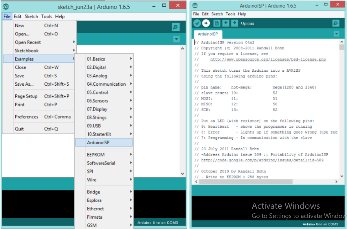
- Connect your Arduino to your computer using a USB cable.
- Open the Arduino IDE and go to File > Examples > 11.ArduinoISP > ArduinoISP.
- To your Arduino, upload the sketch.
- connection of the Attiny45 to the Arduino
- Attiny45 pin 1 to Arduino pin 10
- Attiny45 pin 4 to Arduino GND
- Attiny45 pin 5 to Arduino pin 11
- Attiny45 pin 6 to Arduino pin 12
- Attiny45 pin 7 to Arduino pin 13 refference of the procedure can be captured bellow https://www.14core.com/burning-programming-the-atiny45-or-atiny85-8-bit-mcu/
- To set up the Arduino IDE for Attiny45 process, install the latest version of the Arduino IDE and add the Attiny45 core by going to "File" > "Preferences" and adding the following URL: https://raw.githubusercontent.com/damellis/attiny/ide-1.6.x-boards-manager/package_damellis_attiny_index.json. Then, go to "Tools" > "Board" > "Boards Manager" and install the "ATTinyCore by Spence Konde" core. Select the Attiny45 board by going to "Tools" > "Board" > "ATTinyCore" > "ATtiny45". Choose the programmer you want to use, whether it be an Arduino board or a dedicated programmer, and select it in the "Tools" menu. Finally, write your code in the Arduino IDE and click the "Upload" button to upload it to the Attiny45 using the selected programmer.
- Burning the bootloader is a process of programming the bootloader firmware onto an Arduino board or compatible microcontroller. To burn the bootloader onto an Attiny45 using the Arduino IDE, connect your programmer to the Attiny45 and select it in the "Tools" > "Board" menu. Then, select the programmer you want to use in the "Tools" > "Programmer" menu. Next, go to "Tools" > "Burn Bootloader" to start the bootloader burning process. This process can take a few minutes to complete, and it will overwrite the existing firmware on the Attiny45 with the bootloader firmware. Once the process is complete, you can start uploading sketches to the Attiny45 using the bootloader.
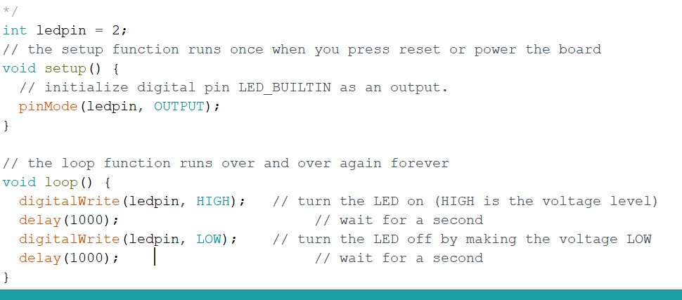
- To test the Attiny45 after programming, you can connect it to an LED and resistor on a breadboard to see if it blinks. To do this, connect the anode of the LED to pin PB0 (pin 5) of the Attiny45 and connect the cathode of the LED to a resistor. Then, connect the other end of the resistor to GND. Once the Attiny45 is programmed, open a new sketch in the Arduino IDE and write the code to blink the LED by setting the PB0 pin as an output and toggling it HIGH and LOW with a delay in between. Upload the code to the Attiny45 and observe if the LED blinks. If it does, then the Attiny45 is working properly. If it doesn't, check your wiring, code, and make sure the Attiny45 is programmed correctly.
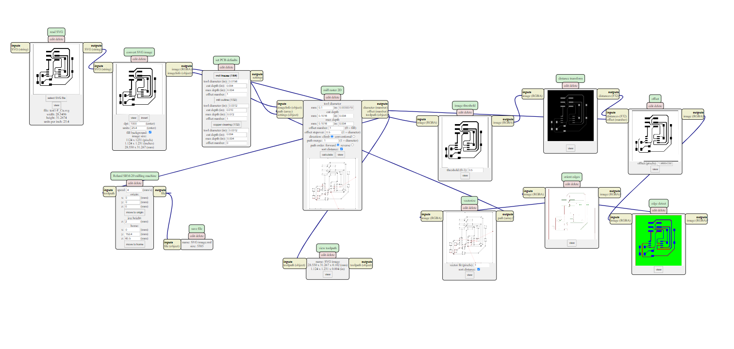
Exporting My PCB BOARD IN SVG FORMAT
Exporting your PCB board design in SVG (Scalable Vector Graphics) format can be useful for sharing your design with others who may not have access to KiCad software or including the design in a document or presentation. To export your PCB design in SVG format from KiCad, you can open the PCB layout editor, select "Export" from the File menu and choose "Export SVG." You can then customize the output file name, layers to be exported, and scale before generating the SVG file. Once exported, you can open the SVG file in a web browser or vector graphics editor for viewing and editing as needed.
afte exporting my pcb board in svg format the is a process used to convert svg into G-CODE
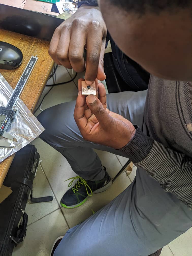

eletronic components soldering on designed pcb
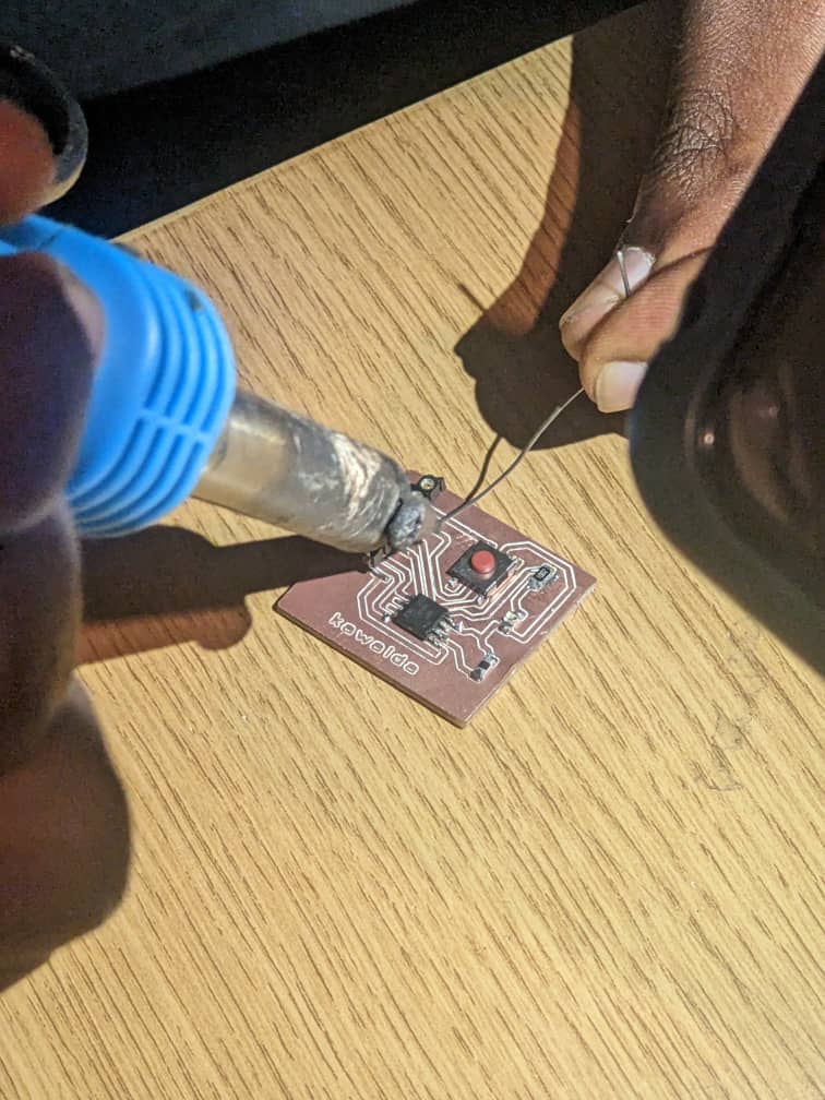
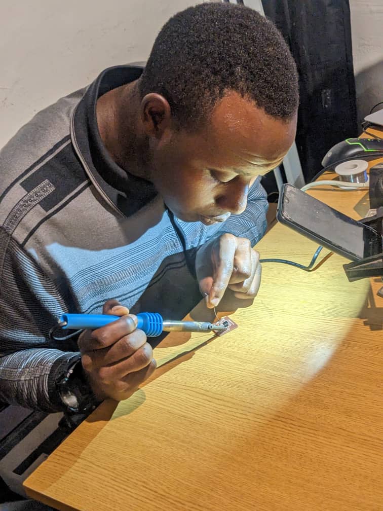
programing of my pcb for briking led
The attiny45's functionality needed to be verified after soldering. Before launching the first sketch, we must first load a bootloader. A microcontroller unit (MCU) or other electrical devices employ a bootloader, which is a short software, to load or initialize the main program or firmware. The MCU's bootloader program is often kept in non-volatile memory, such flash memory, and is launched whenever the device is powered on or reset. The main job of the bootloader is to load the main program into the proper memory locations and initialize the necessary hardware resources in order to set up the MCU for the execution of the main program.
the steps followed to burn bootloader in Attiny45 MCU using Arduino as ISP:Get the Arduino ready as an ISP