ELECTRONICS DESIGN
Work to be done:
# Design a development board to interact and communicate with an embedded microcontroller extra credit: try another design workflow extra credit: make a case for it extra credit: simulate its operation.
# group assignment: Use the test equipment in your lab to observe the operation of a microcontroller circuit board
INTRODUTION ON ELECTRONICS DESIGN :
Electronics design is the process of creating electronic circuits or systems that perform a specific function. It involves designing and assembling electronic components such as resistors, capacitors, diodes, transistors, and integrated circuits (ICs) to create electronic circuits that can process, store, and transmit information. The electronics design process typically involves several steps, including circuit design, component selection, schematic capture, PCB layout, prototyping, testing, and manufacturing..
Here is What we do in Electronic design:
1.Circuit design: This involves creating a schematic diagram of the electronic circuit that you want to build. You will need to choose the appropriate electronic components and connect them together in a way that achieves the desired functionality.
2.Component selection: Choosing the right components is critical to the success of your electronic design. You will need to consider factors such as the component's electrical properties, size, cost, and availability.
3.Schematic capture: This involves creating a digital representation of your circuit design using software tools such as Altium Designer or Eagle PCB. The schematic captures the connections between components and helps to ensure that your design is error-free.
4.PCB layout: Once you have your schematic, you will need to lay out the physical design of your printed circuit board (PCB). This involves placing the components and routing the connections between them to create a compact and efficient layout.
5.Prototyping: Before moving to full-scale production, it's a good idea to build a prototype of your electronic design to test its functionality and performance. You may need to iterate on your design and make adjustments based on your testing results.
6.Testing and verification: Once you have a working prototype, you will need to test and verify that your electronic design meets the desired specifications. You may need to use test equipment such as oscilloscopes, multimeters, and logic analyzers to measure the performance of your circuit.
7.Manufacturing: Once your design is finalized and tested, you can move on to manufacturing your electronic product. This involves sourcing the components, creating the PCBs, and assembling the final product.
Choosing a software to be used in Electronic Design:
I will work with KiCAD software since it is well supported on the windows that I use everyday. I also like that KiCAD is a free software, so it doesn't limit me on how big my circuit board can be. I used KiCAD because I want to learn it more so I can continue to use it even after fabacademy for my personal work..
PCB Design Workflow (Steps by steps)
Designing PCB
1.Schematic design: Create a schematic of the circuit you want to build. This can be done using a schematic capture software. The schematic captures the components and connections of the circuit in a graphical representation.
2.Component selection and placement: Select the components you need for your circuit, taking into consideration factors such as availability, cost, performance, and reliability. Once you have your components, place them on your schematic in a logical and organized way.
3.Netlist generation: Generate a netlist, which is a list of all the connections between the components in your schematic. This will be used by your PCB design software to route the connections between the components.
4.PCB layout design: Import the netlist into a PCB design software and lay out the physical placement of the components on the board. The software will generate a basic layout, but you may need to adjust it to optimize the layout for space, noise, and other factors.
5.Trace routing: Connect the components with copper traces, which can be done manually or automatically by the software. Take care to ensure that the traces are the appropriate width and thickness to carry the required current and minimize noise.
6.Via placement: Add vias to connect traces between different layers of the PCB. Vias are small holes filled with metal that connect the top and bottom layers of the board.
7.Plane generation: Create ground and power planes to provide a stable reference voltage and reduce electromagnetic interference.
8.Design rule checking (DRC): Run a design rule check to ensure that the layout meets the specifications of your manufacturer and is free from any design errors.
9.Gerber file generation: Generate Gerber files, which are industry-standard files used to manufacture the PCB.
10.PCB fabrication: Send the Gerber files to a PCB manufacturer to produce your PCB. The manufacturer will create the board by etching the copper layers, drilling holes, and applying solder mask and silkscreen.
11.Assembly and testing: Once you receive the PCB, you can assemble the components onto the board and test the circuit to ensure it works as expected.
Meaning of PCB:
PCB stands for "Printed Circuit Board". It's a board made of insulating material, usually fiberglass or plastic, on which conductive pathways are printed to connect electronic components like resistors, capacitors, and microchips. PCBs are used to create the physical foundation of electronic devices and are a crucial part of modern electronics manufacturing.
Here are some tools and materials commonly used in PCB design: :
1.PCB design software: There are many PCB design software options available, including KiCad. These software programs allow you to create schematics, layout the board, and generate Gerber files for manufacturing.
2.Computer-Aided Manufacturing (CAM) software: CAM software is used to convert the Gerber files into a format that can be used by the PCB manufacturer's equipment to fabricate the board.
3.Components: You will need to select and purchase electronic components such as resistors, capacitors, diodes, and integrated circuits for your circuit. These components come in different package sizes and types, and you will need to select the ones that are suitable for your design.
4.PCB substrate material: The most common substrate materials used in PCBs are fiberglass, ceramic, and plastic. The choice of material depends on the requirements of the circuit, such as size, weight, and operating environment.
5.Copper foil: Copper foil is used to create the conductive traces on the PCB. Copper foil comes in different thicknesses and widths, and you will need to select the appropriate thickness for your design.
6.Solder mask: Solder mask is applied over the copper traces to protect them from corrosion and to prevent solder bridges during assembly.
7.Silkscreen: The silkscreen is a layer of ink that is applied over the PCB to indicate component placement, orientation, and other important information.
8.Soldering equipment: You will need soldering equipment to assemble the components onto the PCB. This includes a soldering iron, solder wire, and a flux pen.
9.Multimeter: A multimeter is used to test the circuit and ensure that it is functioning as expected.
Group Assignment:
Indivisual assignment:
Indivisual assignment was to design and development board to interact and communicate with an embedded microcontroller
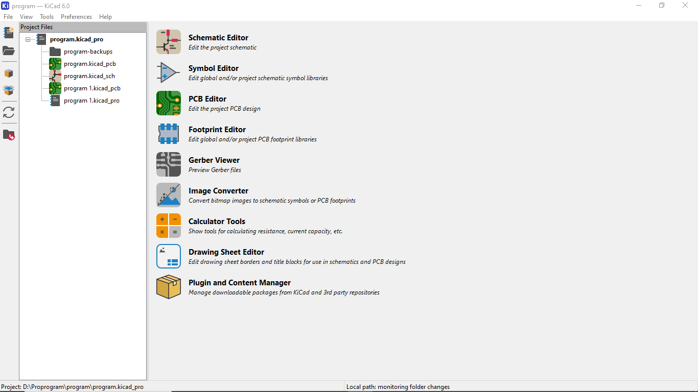
Here i choose to use KiCad couse is an open-source software suite used for electronic design automation (EDA) that facilitates the creation of schematic diagrams and printed circuit board (PCB) layouts
If your are intrested with KiCAD software,
Here is the steps to design PCB using Kcard software:
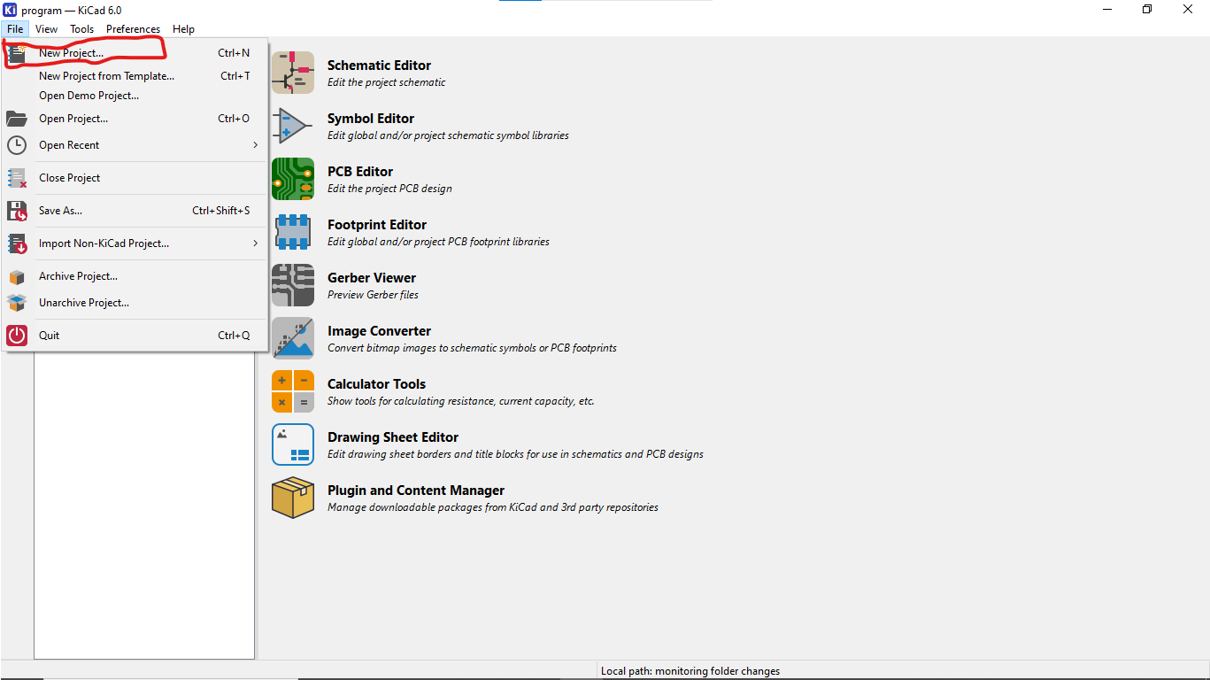
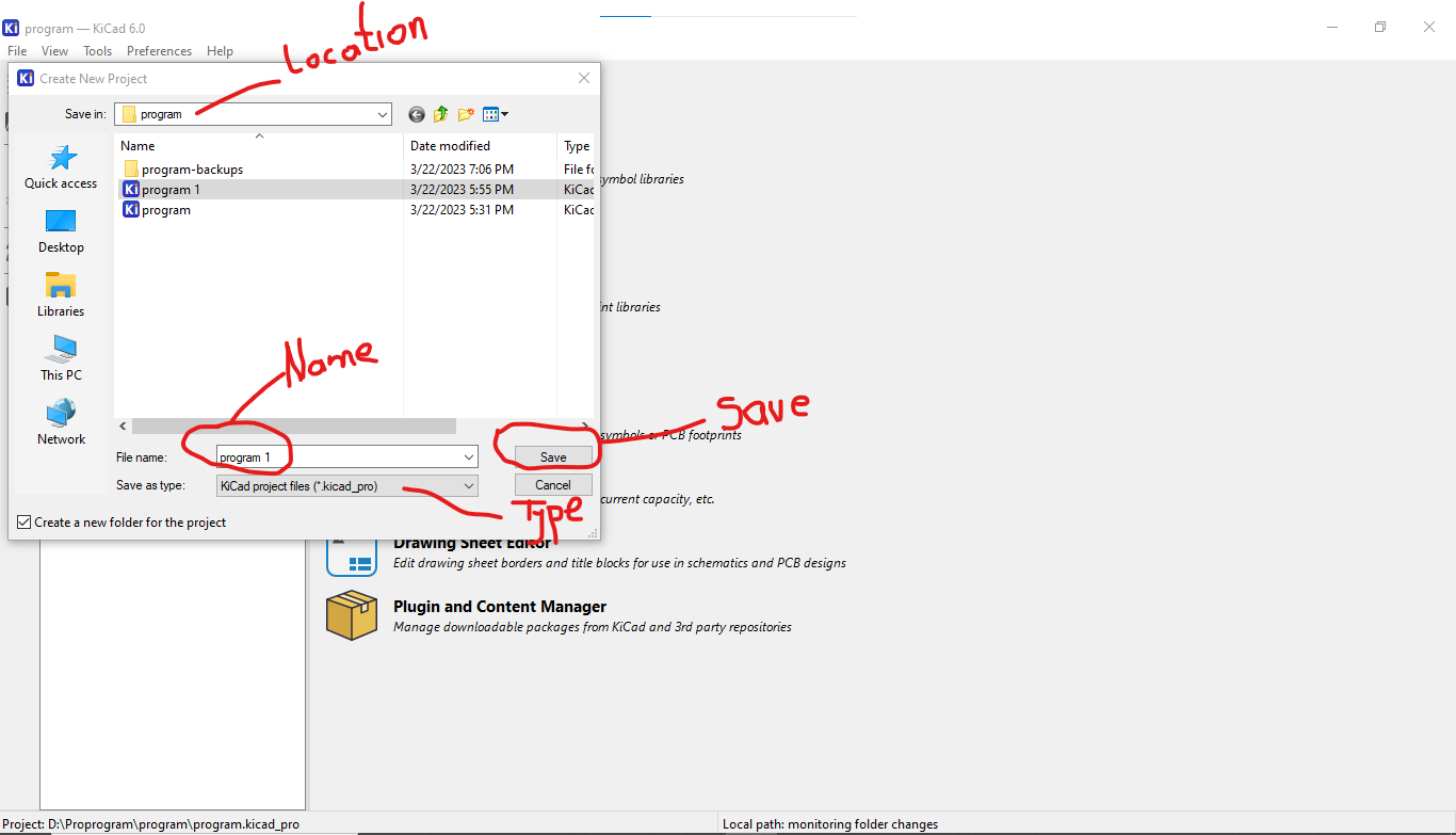
1.Open Kicad software and click on the "Create a new project" button.
2.Name your project and choose a location to save it.
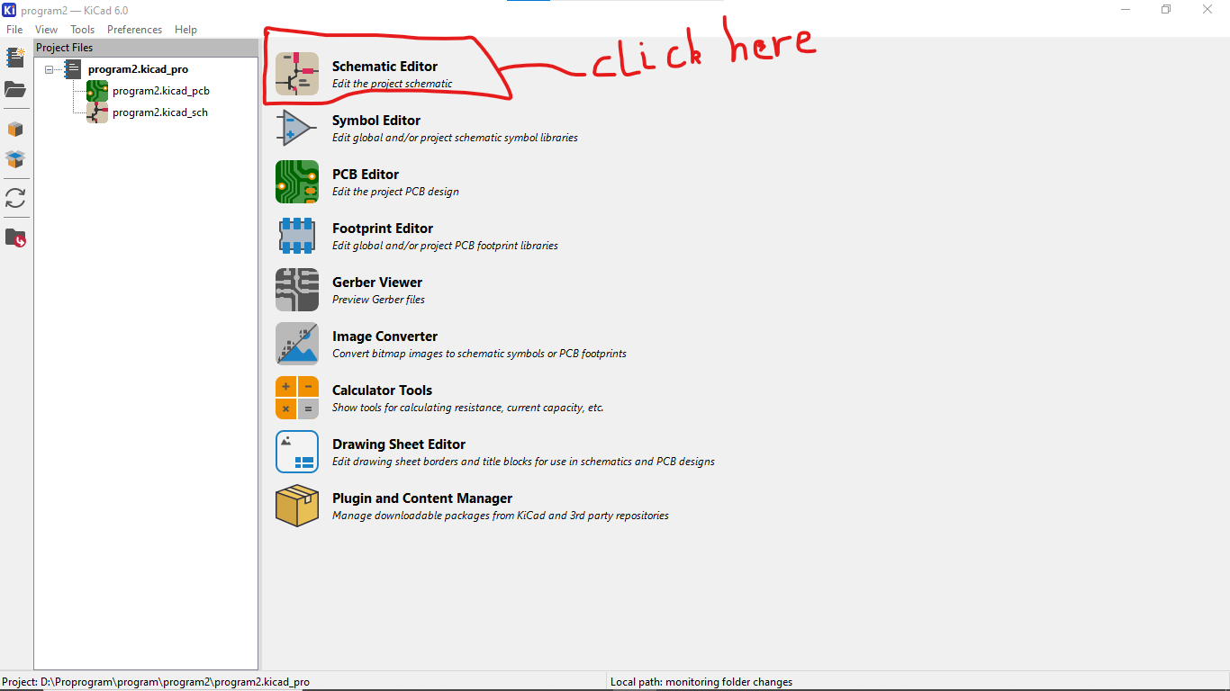
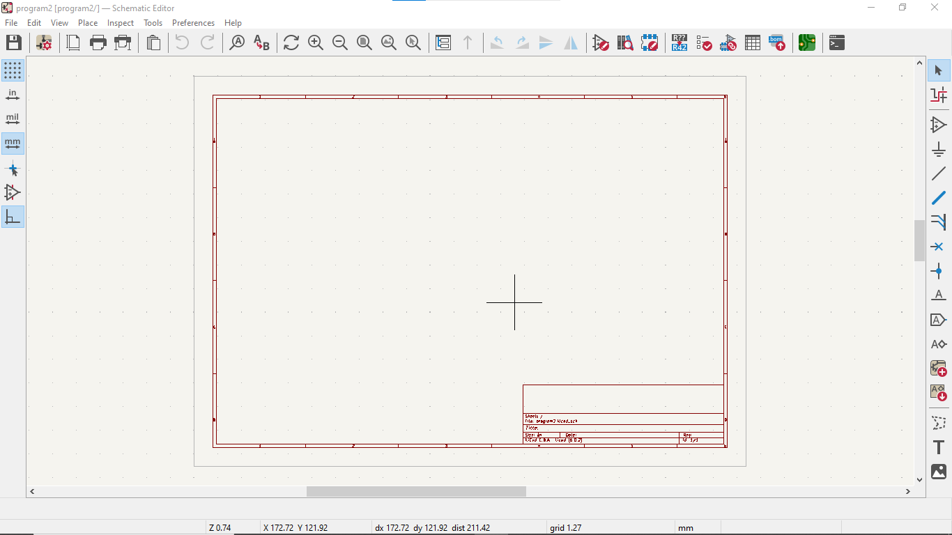
3.Select the schematic editor and create a new schematic.
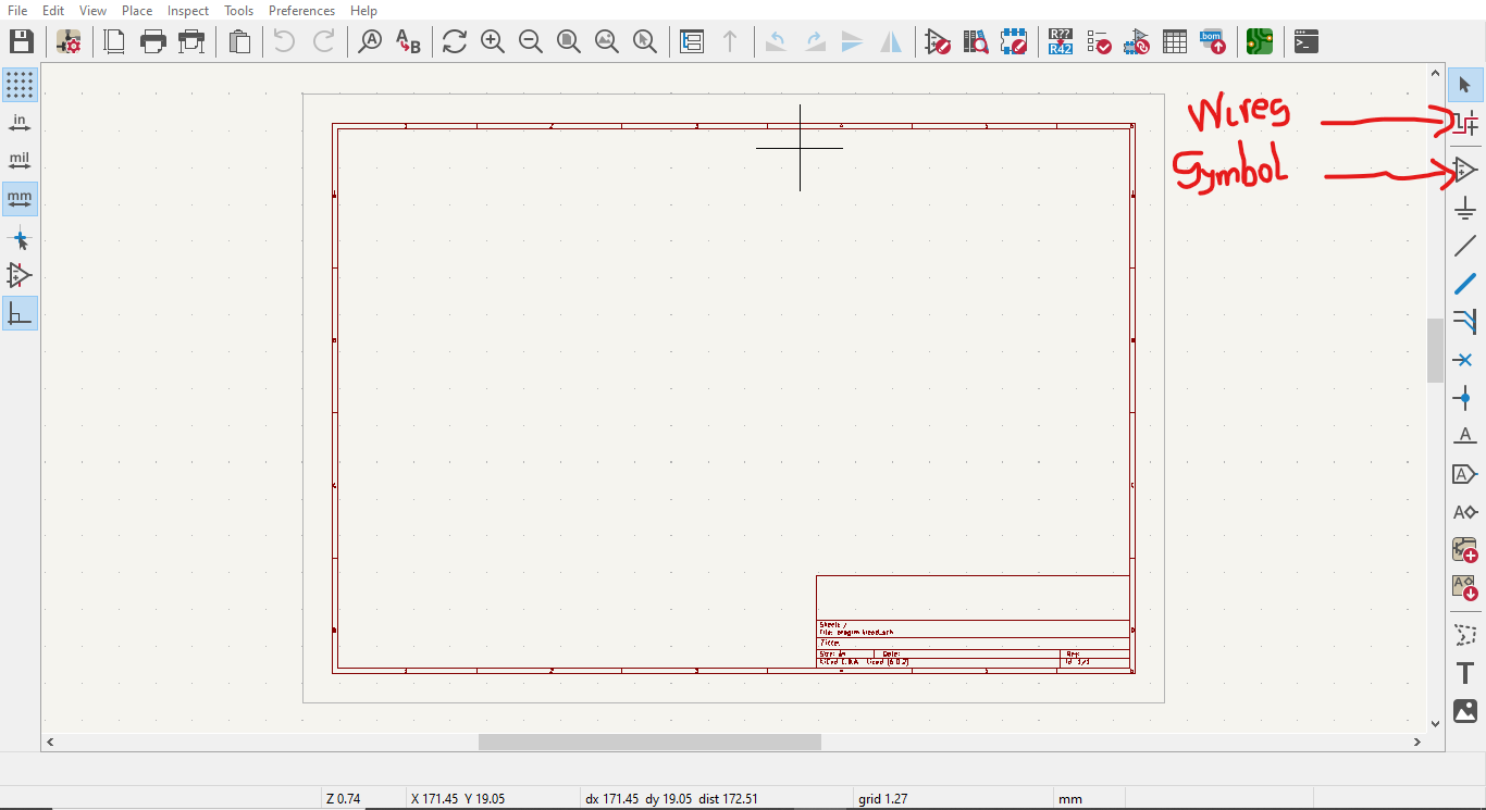
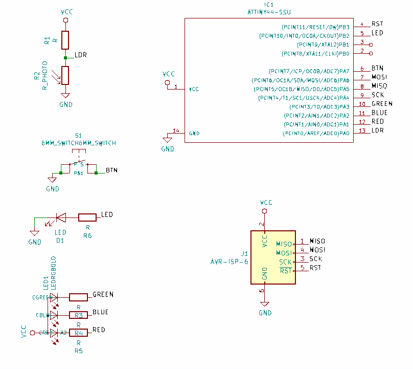
4.Add components to your schematic by selecting them from the library or by creating custom symbols.
5.Connect the components with wires to create the desired circuit.
After, I added all components. Once all components are added the screen looks like this:
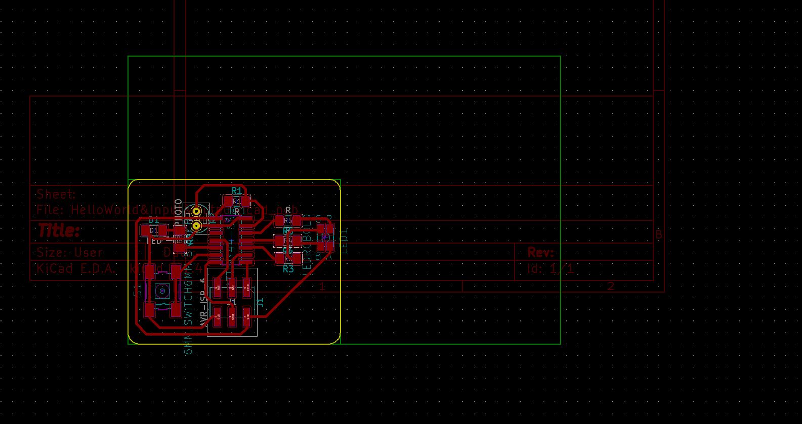
6.After that the next step was to Routing the circuit board as shown in the image below
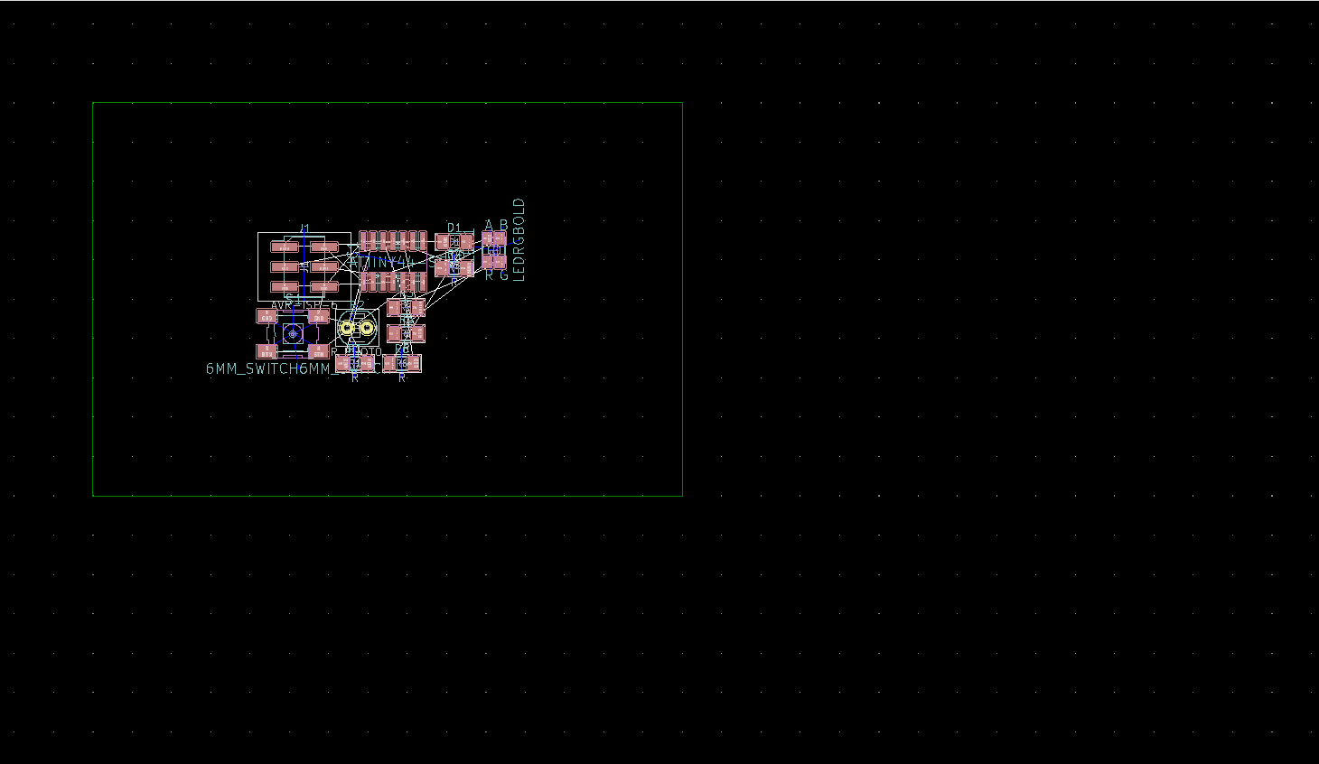
7. Here on this images below i were arraging my components in order to get it connected well

8.Saving the png file image for the traces:
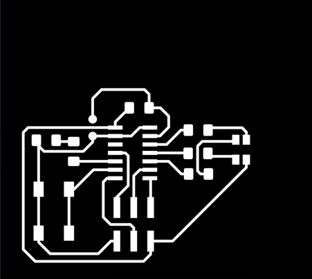
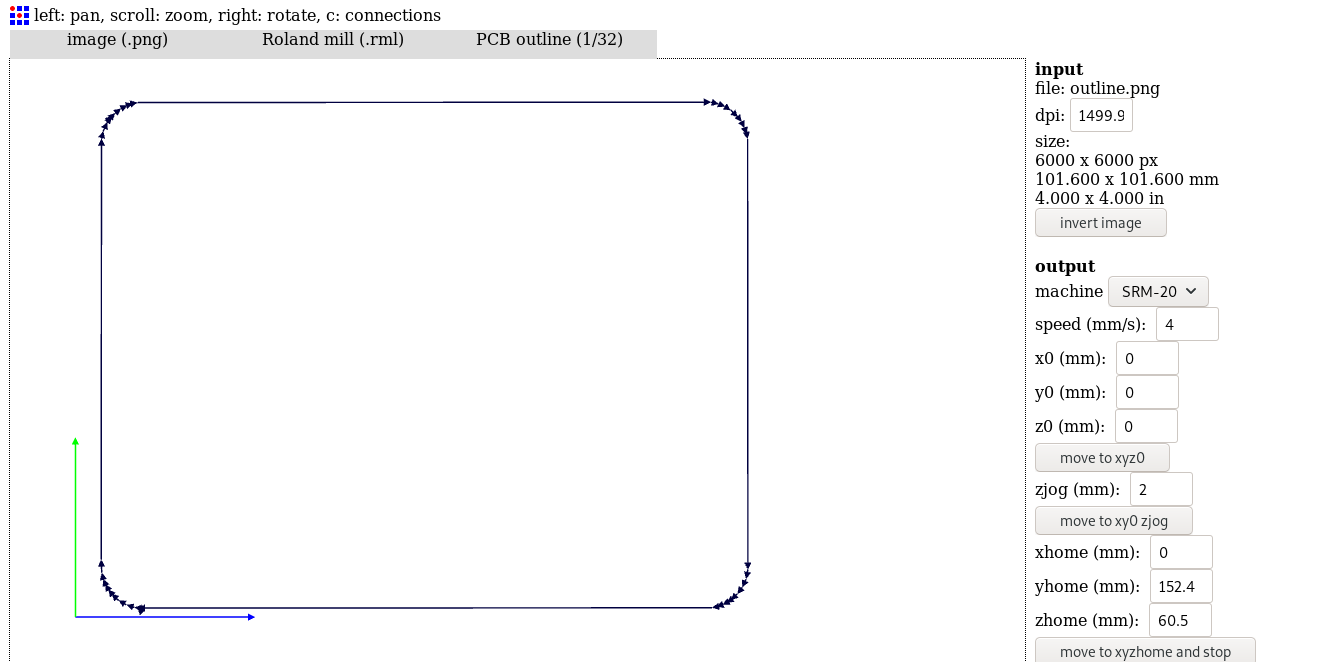
9.Here i Importing the png image in fabmodules to generate the path and .rml file for the milling machine
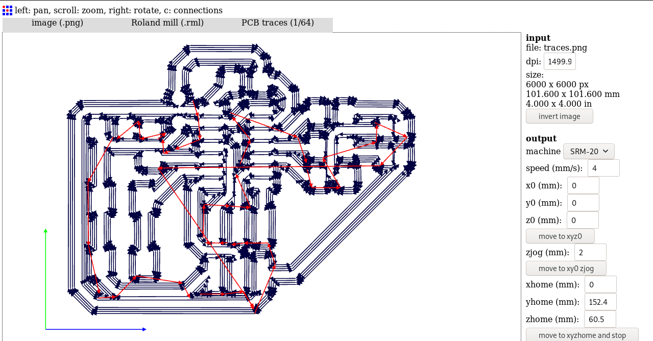
10.Importing the png image in fabmodules to generate the path and .rml file for the milling machine
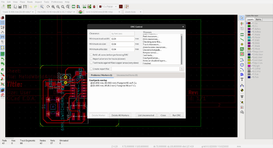
11.Check the design rules (DRC)
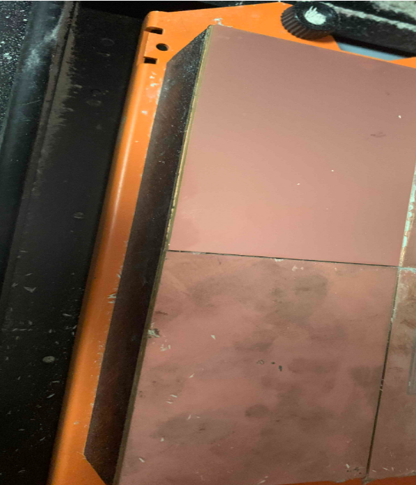
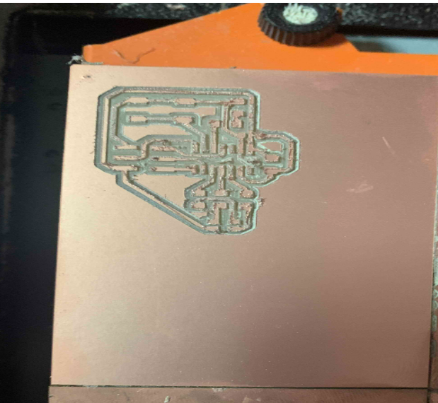
11.Here the next step was to to prepare the bed and fix the RF board with a tape on sacrificial board
12.After milling i check that the traces were done well
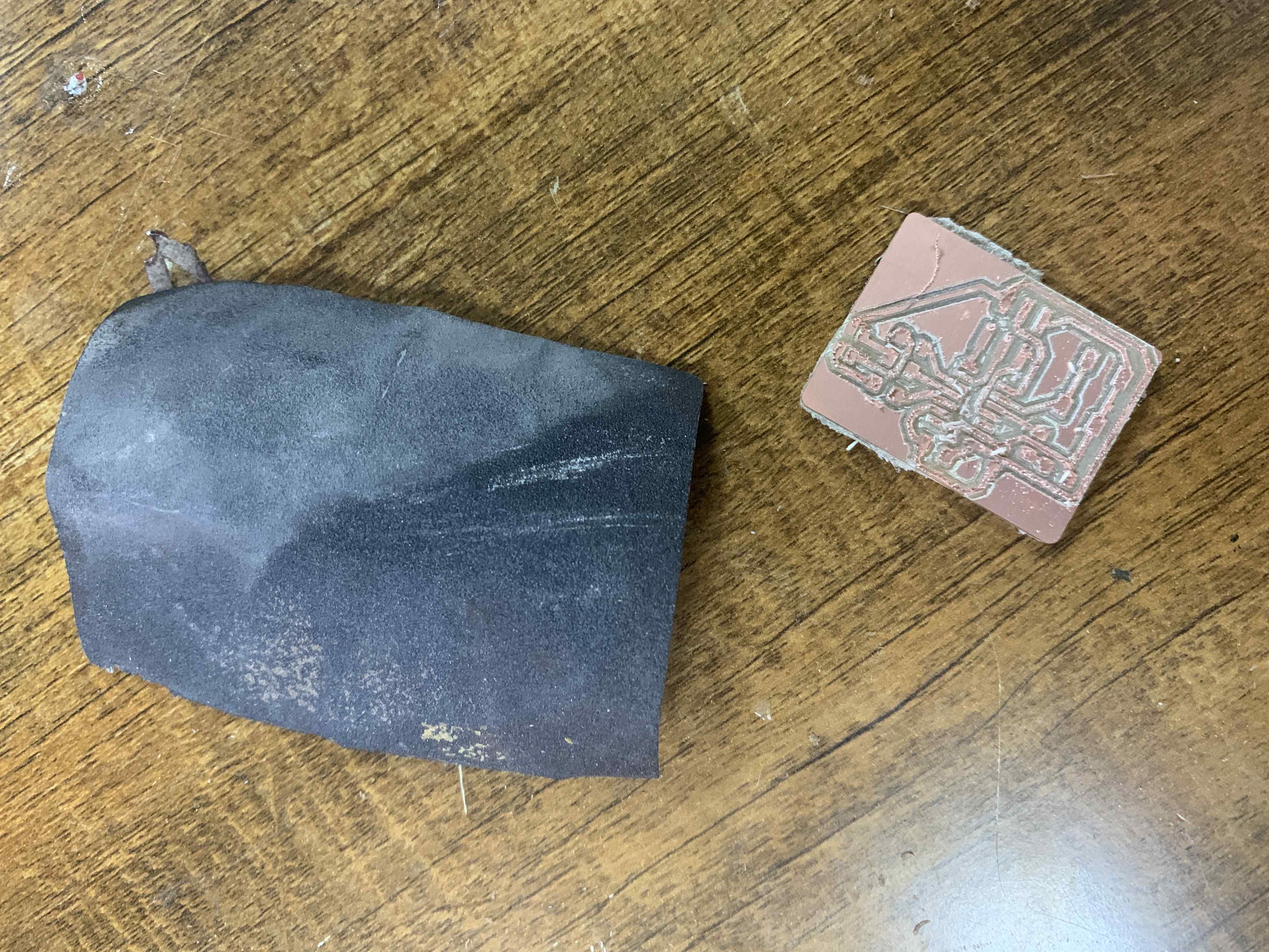
13.After checking I used that black scratcher to remove the top materials.
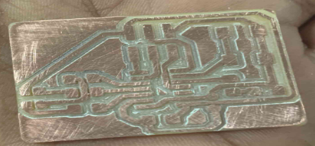
14.Here on this image is how my board looks after creaning it.
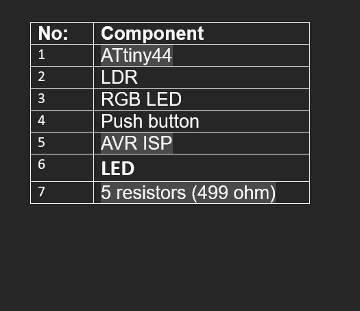
Here is the list of the components to to be added
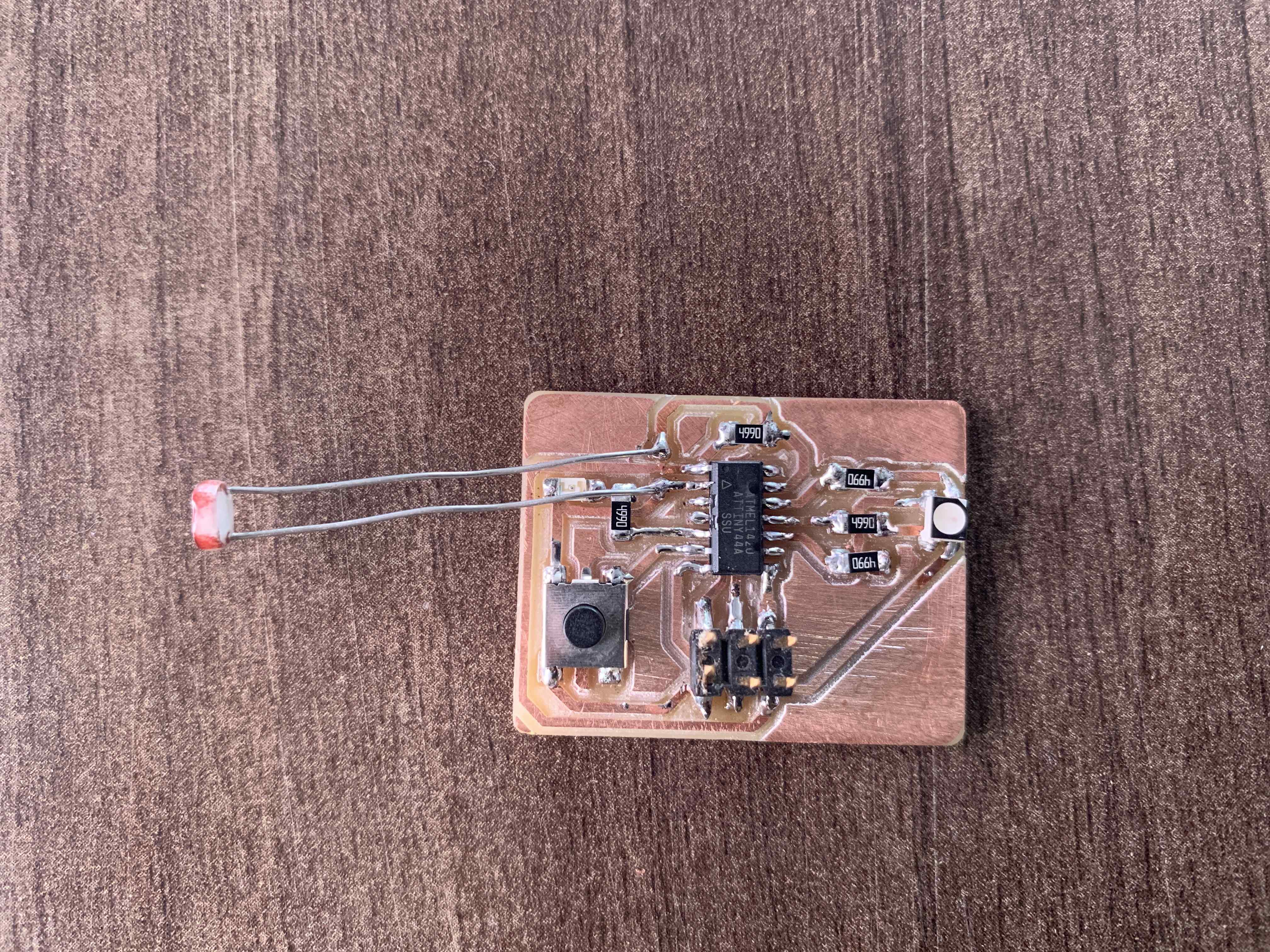
15.Here the next step was to do soldering
Here is the results
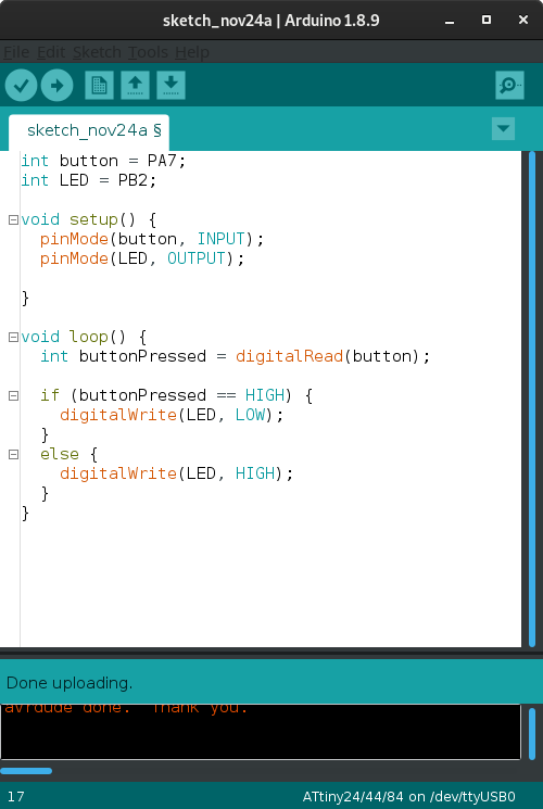
Testing and Uploading the codes