For this assignment I decided to take as a base of my electronic design the ESP32 board, which is “a single 2.4 GHz Wi-Fi-and-Bluetooth combo chip designed with the TSMC low-power 40 nm technology… ESP32 is designed for mobile, wearable electronics, and Internet-of-Things (IoT) applications… ESP32 is a highly-integrated solution for Wi-Fi-and-Bluetooth IoT applications, with around 20 external components. ESP32 integrates an antenna switch, RF balun, power amplifier, low-noise receive amplifier, filters, and power management modules” (ESP32 datasheet, 2023: 1). I decided to use this board because my final project “Chupa Ladxidua” (two hearts) it means to be mobile device or wearable electronics composed of two parts which will send and receive signs between them, both, sound and light. Therefore, I understand that it is necessary to work with a board which has integrated a good a Bluetooth and Wi-Fi solution.
I did my practice in Fusion 360 which is a software containing different applications, among it one for electronics design (former Eagle). To crate a new electronic file first we have to go to file window and then click in new electronic design. This is going to open a new file with 3 different files composing my whole electronic design: 1) Project, 2) schematics and 3) PCB. Then I opened a new schematic where I manage to create a new design using all the tools and design that were previously developed and are storage in the library of the software. However, if those designs for the device are nor stored in the software it is possible to downloaded them from internet, since is very common that providers upload the schematic references of their products. In the case of the SP32 the provider is Spresiff systems. If we go to this webpage, we can find different images with the schematic specifications for this board. When I downloaded this schematic, it was easy to understand how the board was designed. Then is possible to mimic with Fusion 360. For doing that it is important to understand how many pins the board has and how those are connected with other components. To find the connections we have to follow numbers. E.g., IO14 is connected to other IO14. In some cases, green points show that there is a connection among components. We can create also new connections to new components, however is important to be sure that we are not overlapping connections.
Capacitors, those are two parallel lines, it helps you to regulate the constant flux of electricity. Those are normally placed between voltage and ground (GND) to assure the constant flux of energy. Resistance: its icon looks like a lighting. This helps to regulate the flux of energy in order to do not burn our dispositive. Transistors are normally symbolized with an arrow indicating the direction of the electricity flux. Diode: is symbolized with a big arrow. It allows the transit of energy from one direction but not the opposite. A bottom line on the tip of the arow will show you where the energy flux is blocked. If the diode has arrows on the side means that it transmits light. A switch to turn on or off the energy is symbolized like a swing and depending on the side it is you will understand is the energy is always on or off and the direction of it.
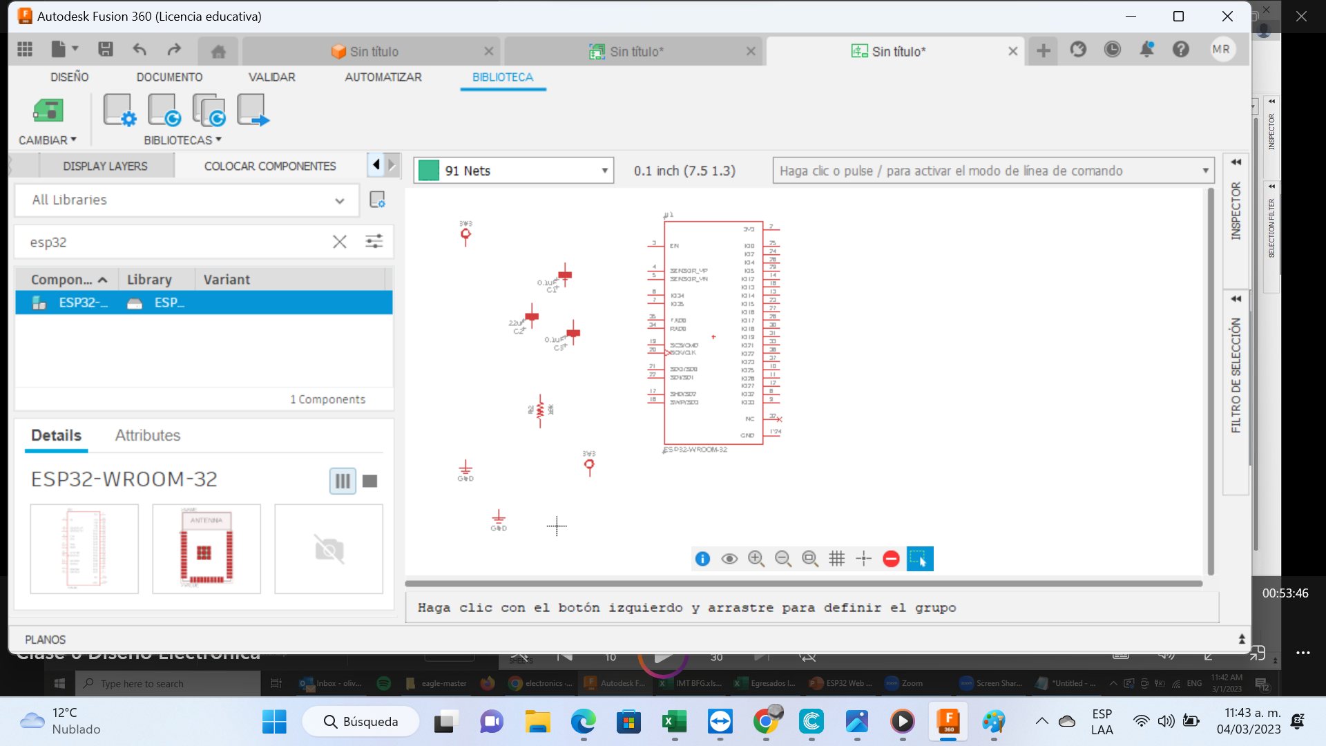
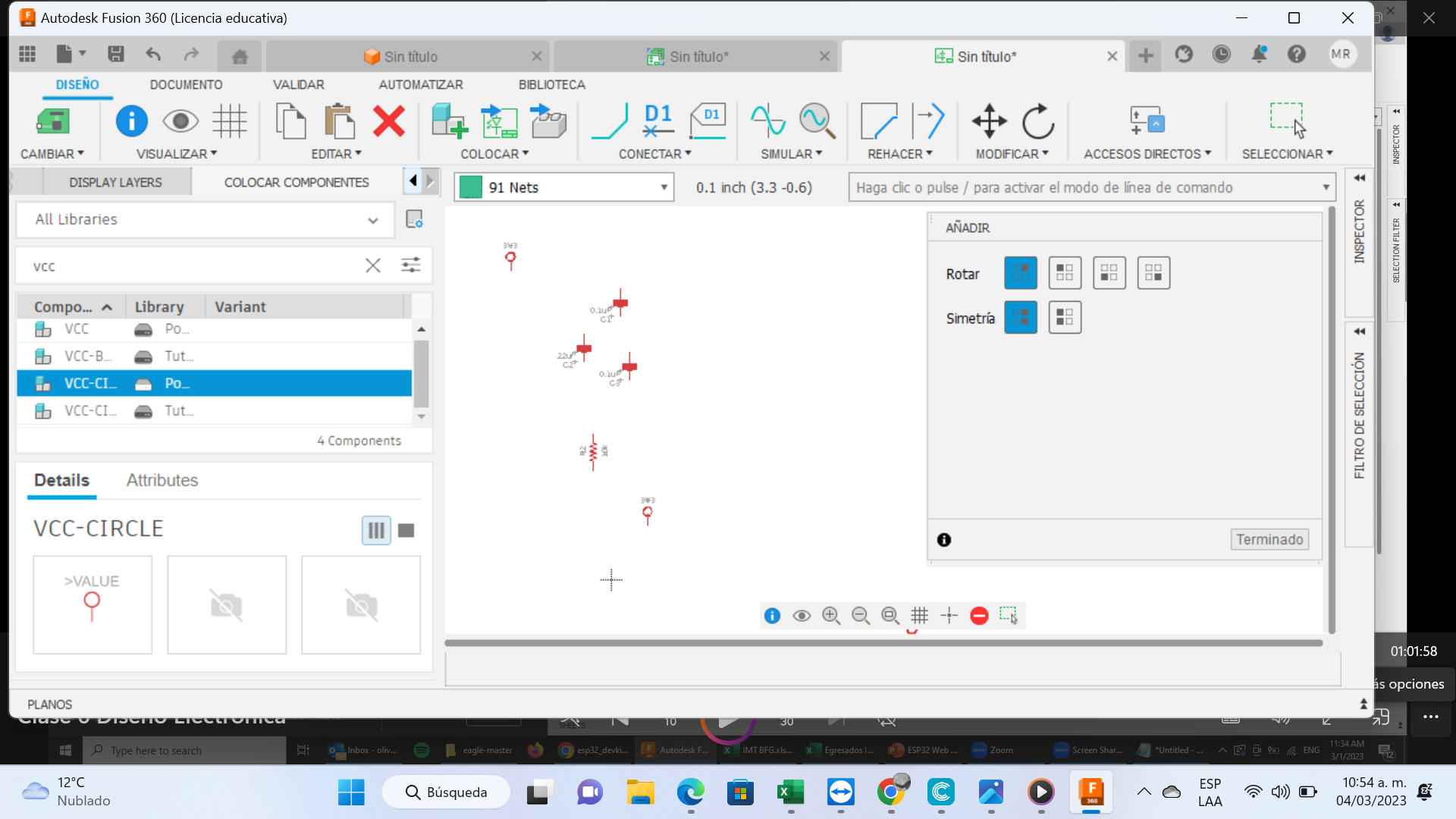
To reproduce a board is recommended to place the schematic we downloaded form internet on one side of the screen and open Fusion 360 on the other. First of all, we look in the gallery the components that we already have. There is a window called “place components” where we can look for all the components in the library. Then I can copy the components I need by being careful of noticing that the schematics of the component, the footprint and the 3d model is what I am looking for. This is shown in the bottom of the page. In this practice I need a superficial food print, not a throw hole (radial), therefore I have to be careful of choosing the right component. Other think important to pay attention is on the size of the component. The recommendation is to work with the 1206 because is kind of big to manipulate and is the most commercial. You can find the right dimension of the schematic design in the “variants” window. Then I choose the right one and placed in the white window. I can put as many components as I want. I can also assign specific values to each component. I can do this with the window “modify”. Then I give a click in “value” and assign it to the component following the main model. Since the ESP32 was not installed in the library of Fusion360 I had to look after it going to library manager. Since I did not find it, I had to go to a web page called SnapEDA which allowed me to look after components that a provider already sketched. There I simply introduce the name of the component and look after it. I have to be careful to choose the sketch of the drawing I am looking for and then I can download the symbol and the footprint for the program I am using to design, in my case Fusion 360. Then we I look for it in the window import libraries, and clink on import from local disk. Once found it is possible to open it and turn it on in the program because normally is off. Then I looked after it on the library and put it in the working space. Then I followed step by step the requirement of the model to make all the connections and to produce the board following all the components I need. To make the wiring I have to go to design and then to net. To make the connections I simply go to the tip of the component and take it to the direction where I want to make the connection. A green line will show when the connection is settled. A green dot also shows when I managed to connect a component to a cable. To be sure that it is well connected I can move the component and be sure that it goes together with the cable. Other way of making the wiring is just by putting together the tip of the components and the cables. I can also put cables with the connection Enable (EN). To do so I have to go to the window EN and use the toll name. In this way by placing the same name between to components I make a connection. When I do such a connection the window enable name have to be active. When the program find that you give the same name to two separated cables it will ask you if you want to connect them, then you just have to click yes. Switch: To connect a switch (tact) you always need to place a resistor next to it. This is because of the relation V=RV, otherwise I will produce a short circuit. Depending on the side of the resistance the switch is going to be in a position of pull up or pull down, the former means that is going to be always on, and the latter always off. Led: In other to put a led the process is the same. First, I go to the library, then I look for a led. I have to choose the right size (1206) and place also a resistance. To make the connection I need to put on one side positive and the other negative and then make all the connections. I have to choose what I what to do with the led. For example, if I want to understand when the board is on then I can enable it to be always on with a connection to voltage. But if I want it to be programable then I can connect it to a free PIN, for example de IO2 to make it blink. The easiest way to do this is by initiating a cable in the led and the PIN and placing the same name on the top of it.
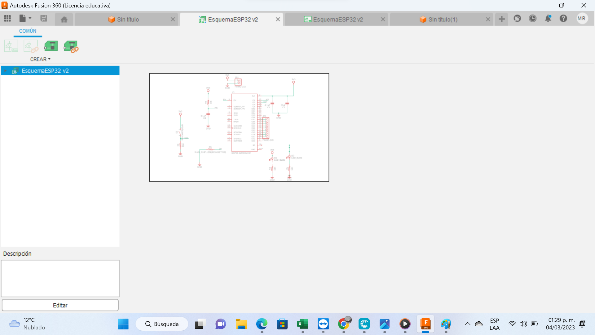
It is a good idea to enable some of the PIN, even though I am not going to use all of them for the moment. To do that I use a Header which allowed me to connect multiple PIN. I choose one to connect 9 PINs. To make the connection faster I just placed my PIN header over the free pins in the board and then make a space between the two elements. The last componet I added was a header of 2 in order to enable the power to come into my board. Again, I have to connect it to Voltage and ground. Other option could be to place a USB and connect it to voltage and energy. In this way I can connect it to my computer and use it a source of energy at the same time. To finish the schematic design, I have to save it and put a name.
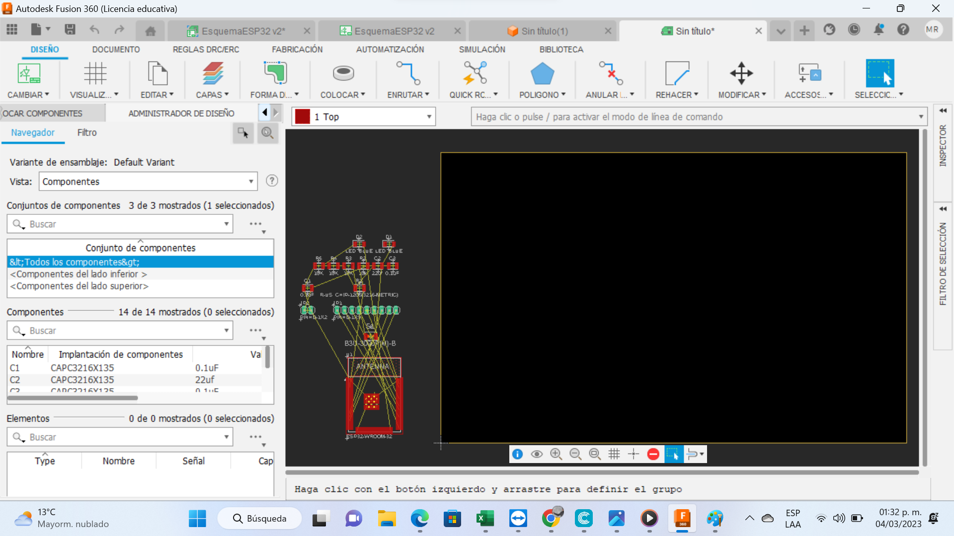
To sketch the board first I come to the window of my project. There I can find the schematic design wich I have to place it inside the frame on the right side. Then I have to click on the There is going to be displayed a black window with the schema of our PBC by colors. Each color has a meaning which I can discover in the left side of the screen.
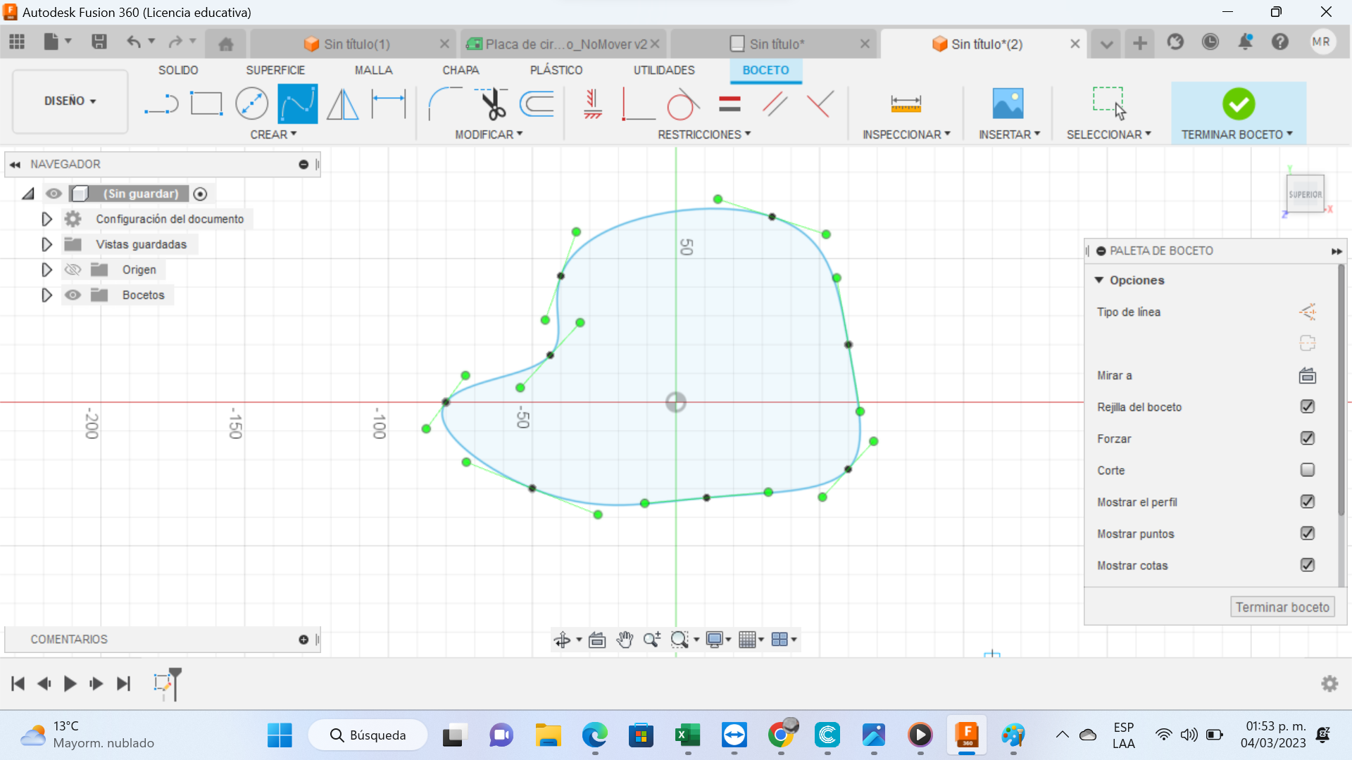
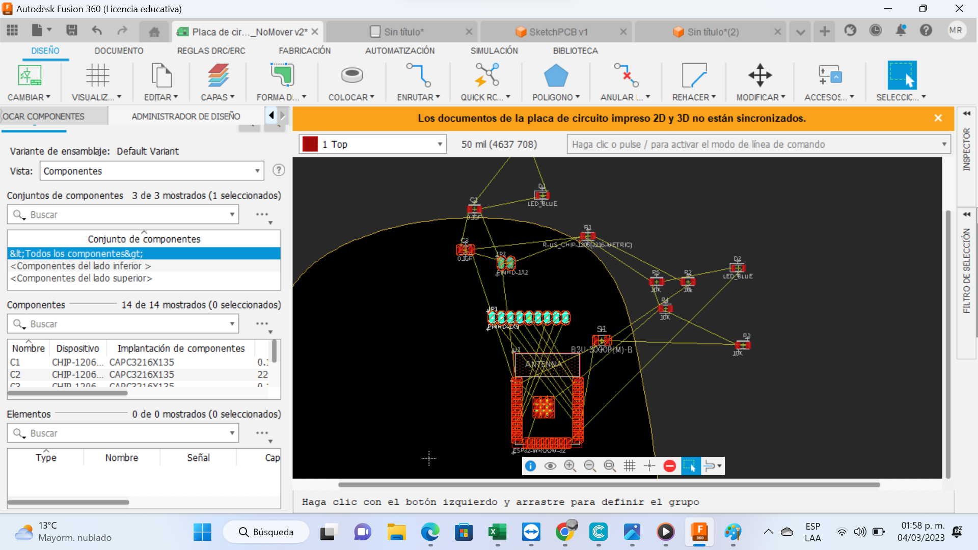
Then I have to put all the schema into the framed black box. Before starting the weirding, I have to give the right shape to the schematic design, otherwise is not going to be possible to produce it. The recommendation is to don’t cross the yellow lines or to do it as few as possible. There is not and automatic way of doing it. Only wiring can be automatic but not the final ordered design. To make the wiring I have to go to route and then to manual. Then I just make click among the connections I want to do. I have to do that with all the yellow lines until I manage to turn all red, that means that all are well connected. If connections are very difficult to make then the best option is to come back to the schematics and modify certain connections form there. Finally, I have to save all and then we go to the window file and to the window new design. There I have to go to file, new design, sketch, and there I can make the form of the board I want. Then I go out of the sketch. Click on create, create PCB, create associated PCB, save it and select all the 3d image of the board. In order to connect this image to my schematic design in 2d I have to go to the window where this is enabled: link 2d PCB (the image of a chain above modify).
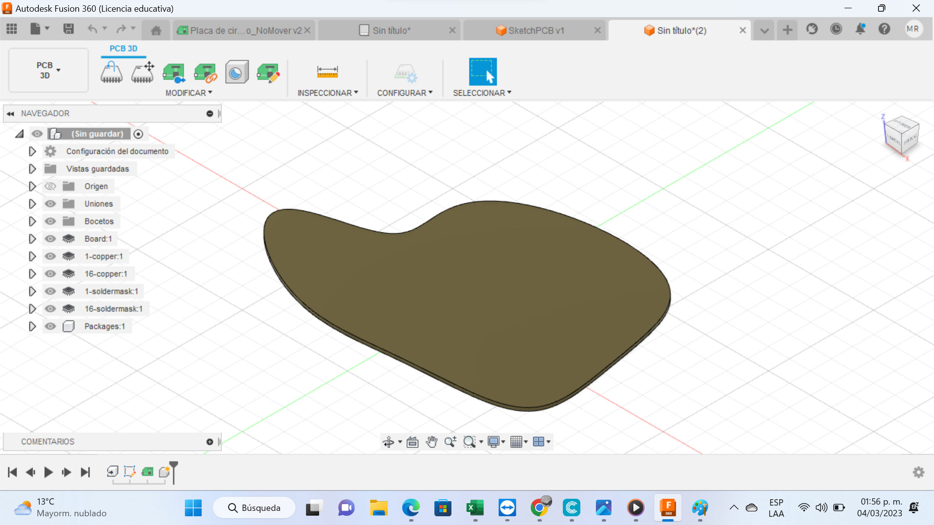
The program will ask me to which I want to make the link and then I select the last design of my PCB. Once is linked, I will have on the same window the 3d PCB and the 2d schematic design. If it happens that is not possible to sync the then I have to go to the up left side of the window and click push. This means that I am making actualizations. Then I can place all the elements of the schematic design wherever I want on the PCB. I have to sync any modification I made between the 3d and the 2d models.
There are 2 design rules I have to follow when I make a PCB: 1) the difficulty of its production. Since I am going to use a “mini mill” if lines are to narrow or there if very few space among them maybe I will not succeed. 2) How much electricity I want to transport. To calculate that we can make use of a webpage called www.4PCB there I can place the current and the thickness of cables and it makes the calculation of which is the minimum to make it function. Other option is to set up the rules DRC in advance. There I can set up a minimum clearance of 12. In size I can make it bigger as well to make it easer the soldering process (trace wide). For example, 28 mil. Last recommendation is to develop a once face PCB and not a 2 face, otherwise it can be to complicate for artesian fabrication.