Electronics Production
Week 8 - Documentation
For this week, we are going to work on electronics production. The idea is to use what we learned in the electronics design week to make an actual board, so we can start connecting our projects.
Software and Equipment:
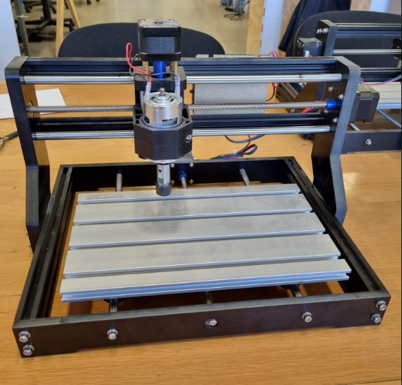
- Machine: Mini Router CNC 3018 PRO
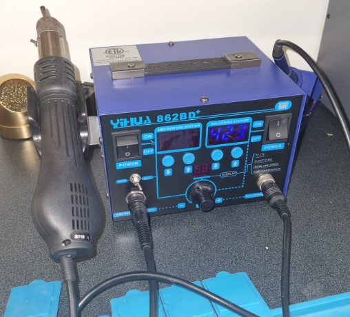
- Machine: Soldering Station
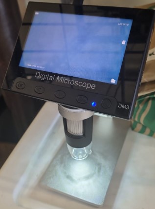
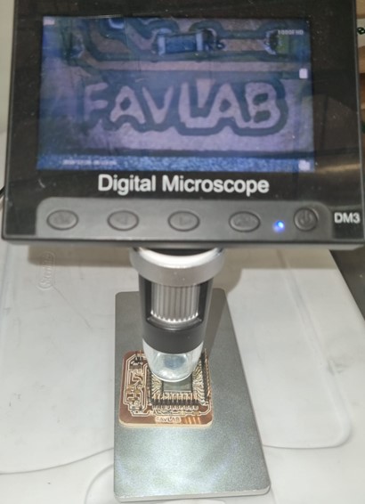
- Machine: DM3 Digital Microscope
- Electronic schematich Software: Fusion 360
- Manufacture Process Software: Mods
- Material:
Mini Router CNC 3018 PRO:
Soldering Station:
Digital Microscope:
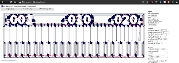
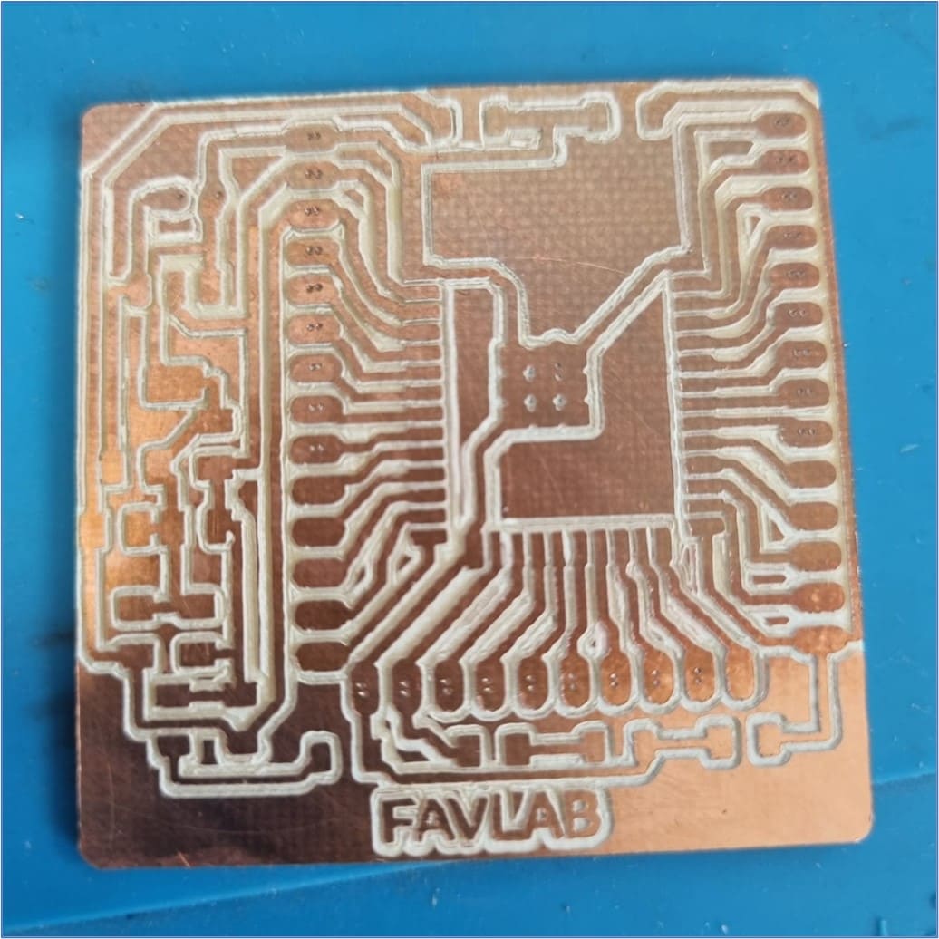
PCB Parametrization
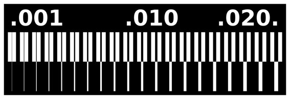
For the PCB parametrization, we designed a PCB board where we change the route and gap from 0.001 to 0.02in.
Now, we use Fabmodules to get the .nc file.
We machine the PCB.
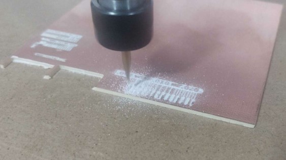
This is the result:
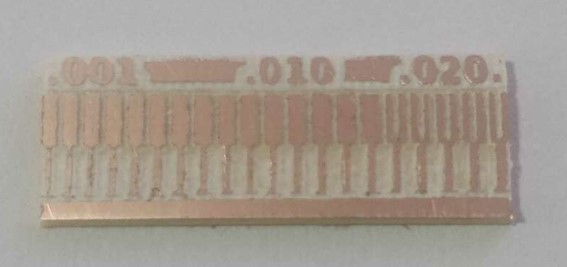
By analyzing the PCB, we can determine that the smallest gap can be 0.016in and that the routes can go as small as 0.001in.

Redesingning my circuit
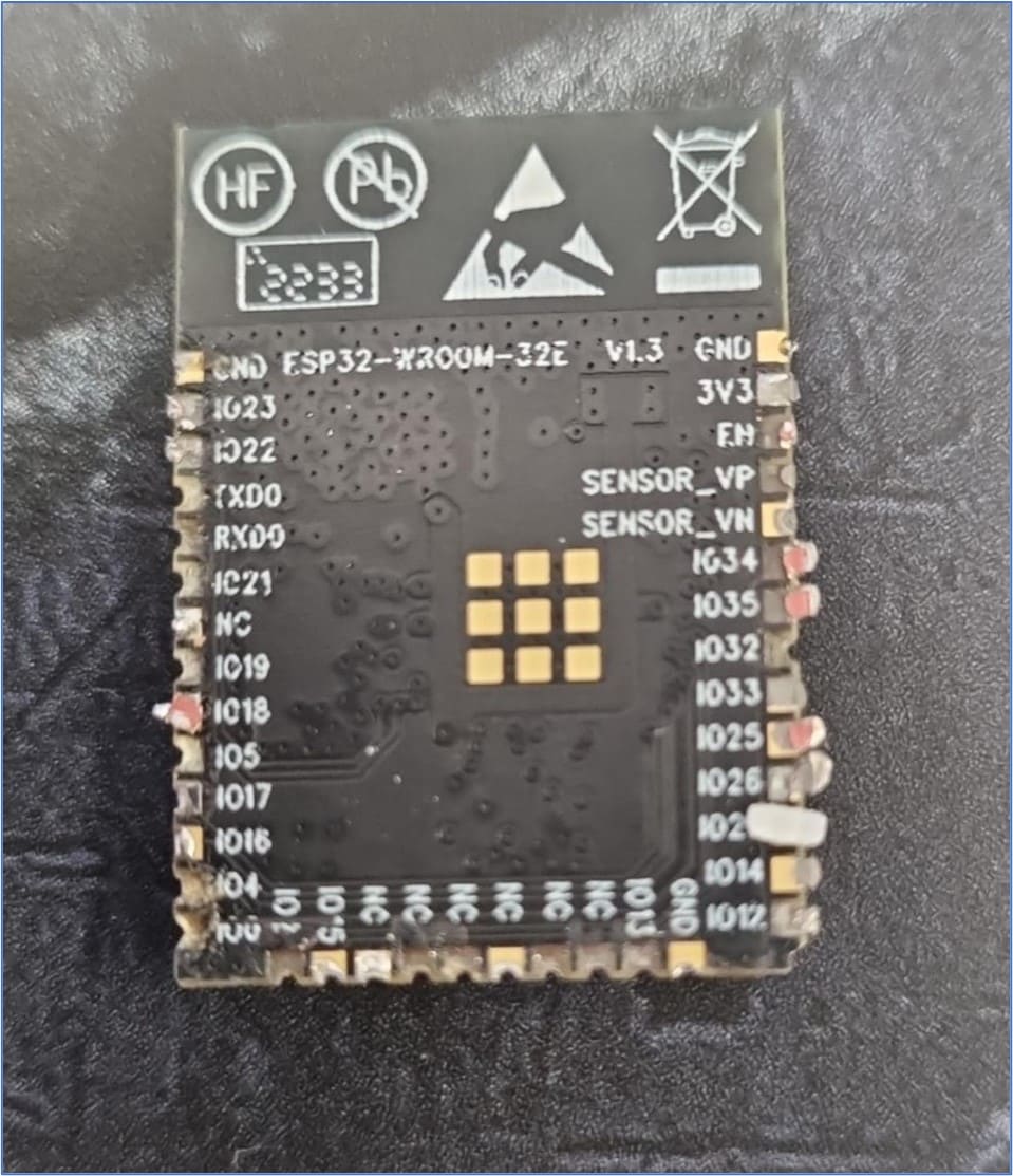
Instead of using a Xiao SAMD21 and a Bluetooth module HC-05 I'm going to use an ESP-WROOM-32 for my project.
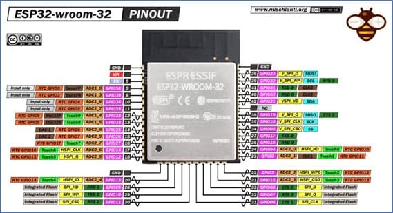
Image taken from: michianti.org
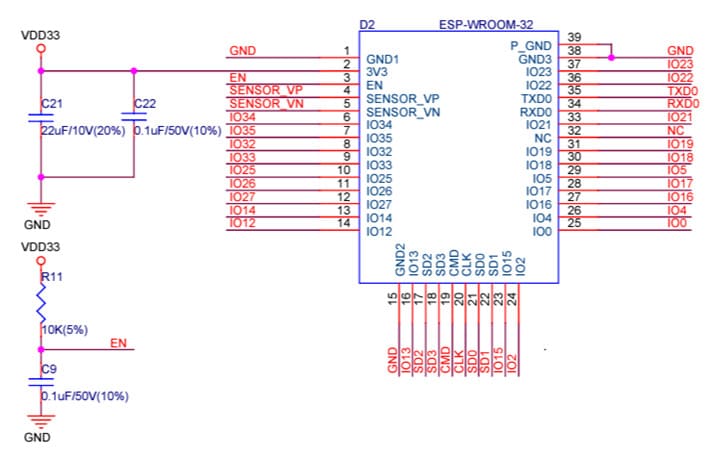
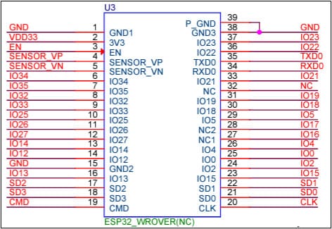
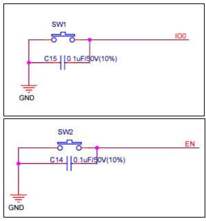
The following diagrams are for the electronics schematic:
Esp32-Wroom-32
Switch buttons
Connectors
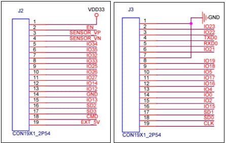
Diagrams taken from Espressif-esp32_devkit
Input voltaje regulator
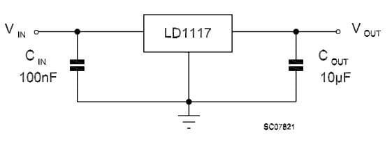
Diagram taken from LD1117V33-TO-220
Design process
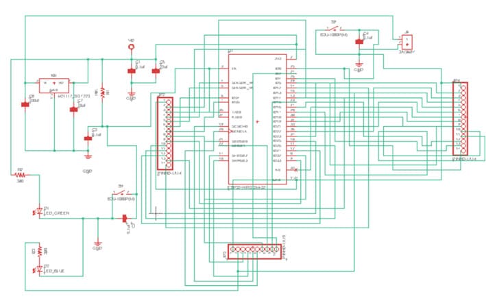
Using the diagrams shown before, I can start designing my own board. My goal is to have this board as a dev kit, so I will make all the connections necessary to have all the pins available. I won't explain the whole process of the designing because it's the same as what we have done in week 6, so if you are interested on reading more of it, go check the electronics design week.
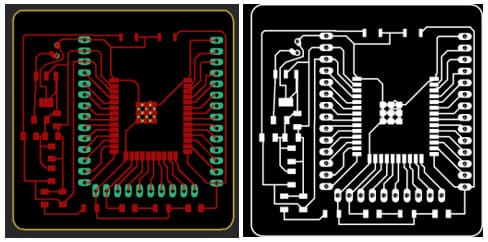
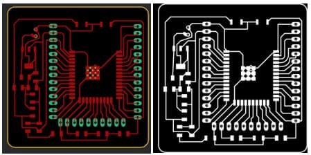
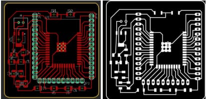
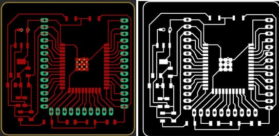
Electronic Schematics:
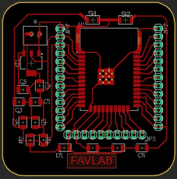
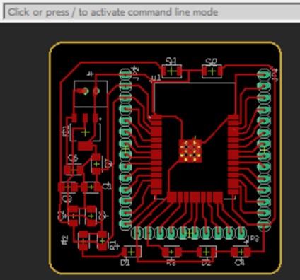
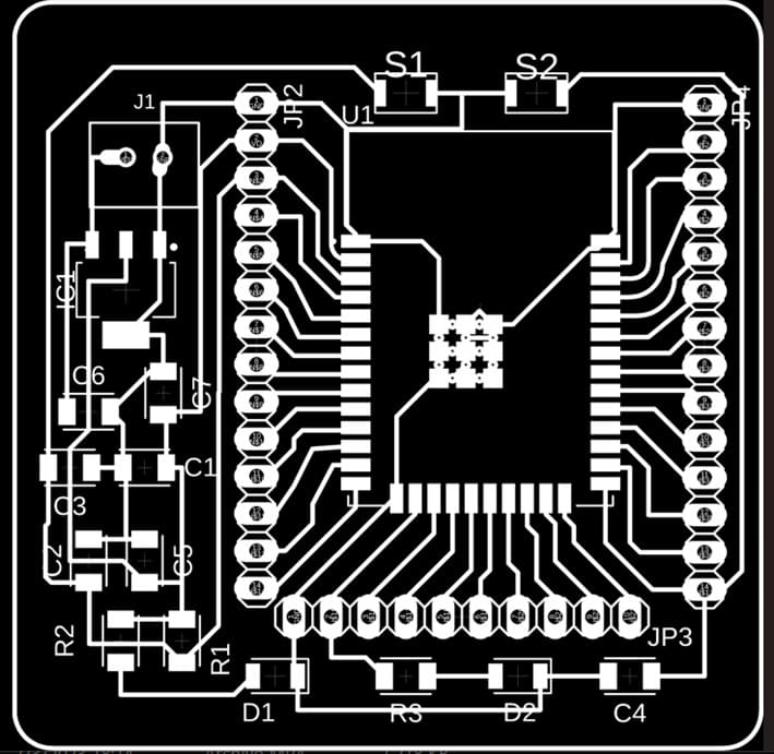
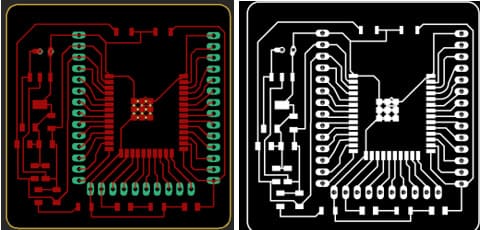
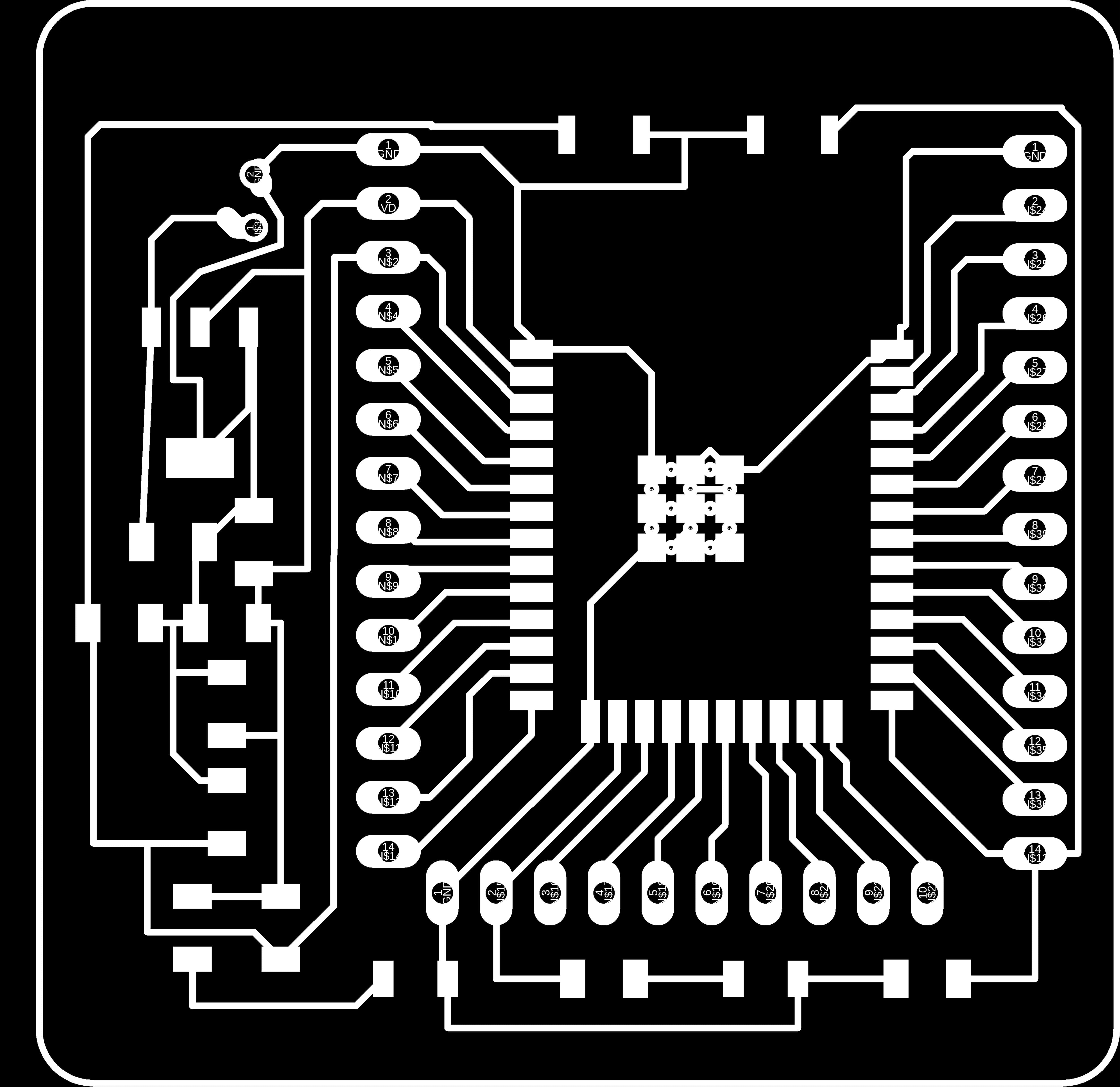
2D PCB Final Design:
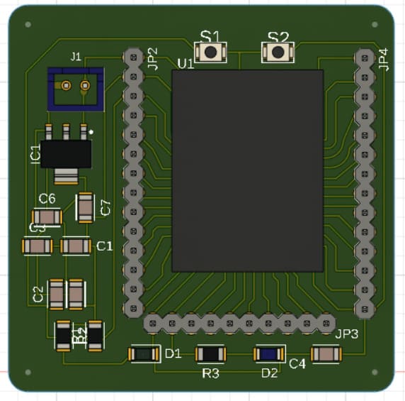
3D PCB Design:
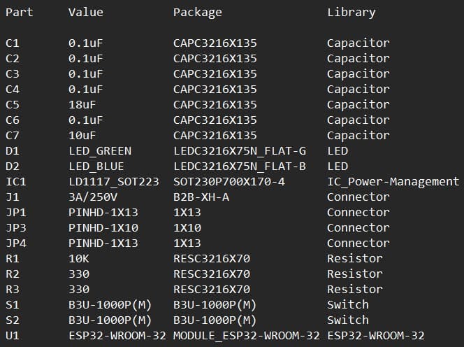
Part List:
Setting up my electronic board
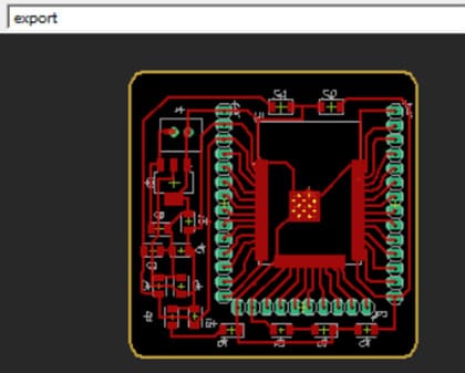
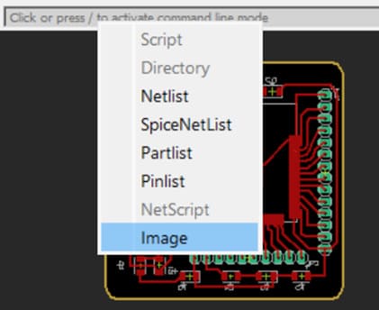
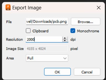
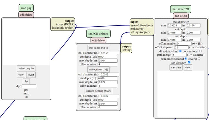
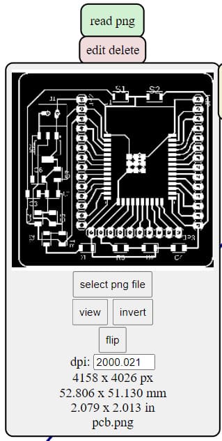
You will need to save the 2D PCB as an image to use it later, so follow the next steps:
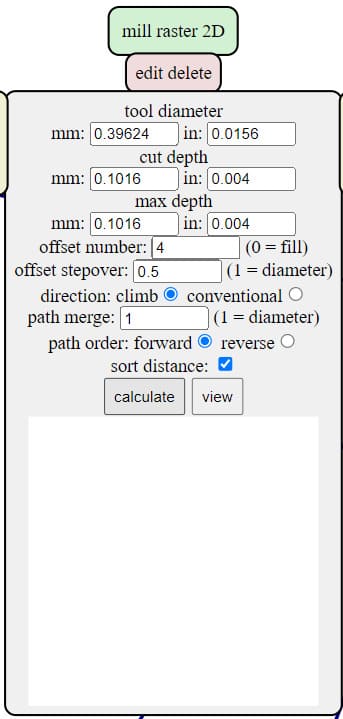
Getting the final PCB design
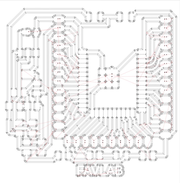
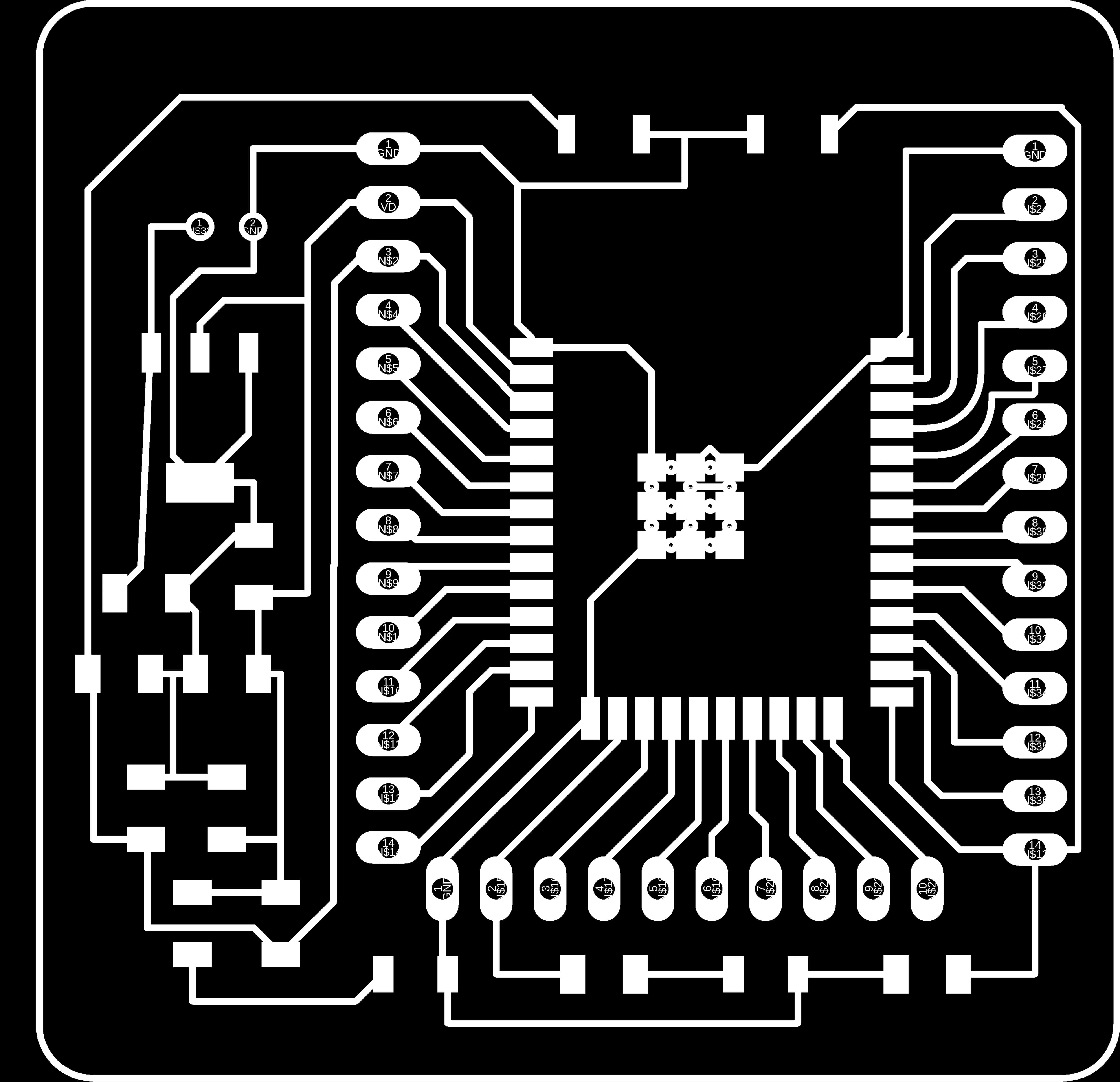
Previously, I showed you how the final PCB board would look like, but to get to that result there were many unsuccessful attempts. Figuring out if the design was going to work required a careful overview of the PCB simulation made in Mods.
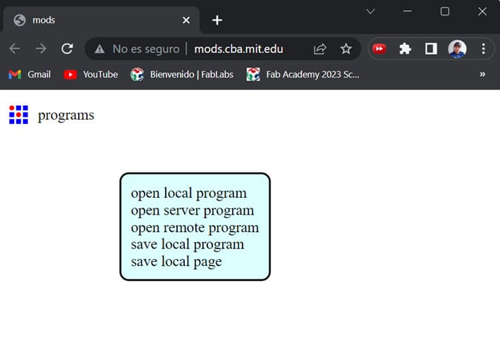
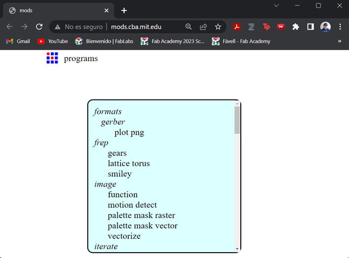
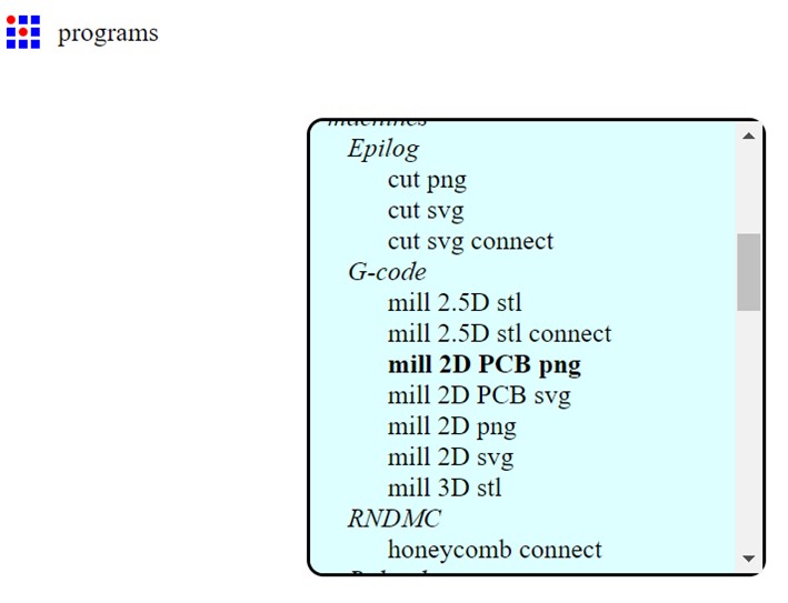
So before going to the attempts, lets check out Mods.
Getting the final PCB design
Previously, I showed you how the final PCB board would look like, but to get to that result there were many unsuccessful attempts. Figuring out if the design was going to work required a careful overview of the PCB simulation made in Mods.
So before going to the attempts, lets check out Mods.
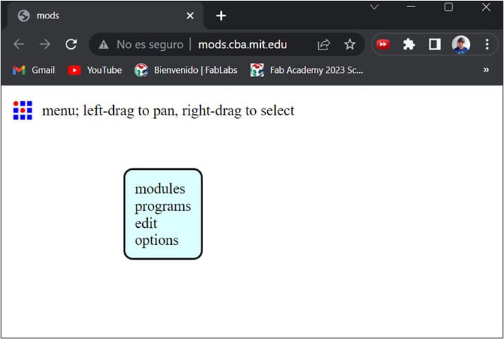
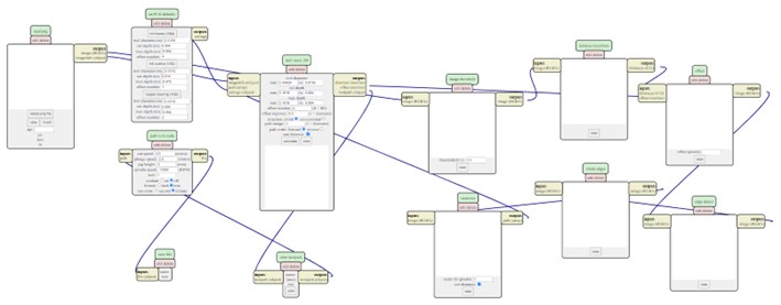
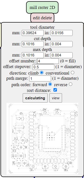
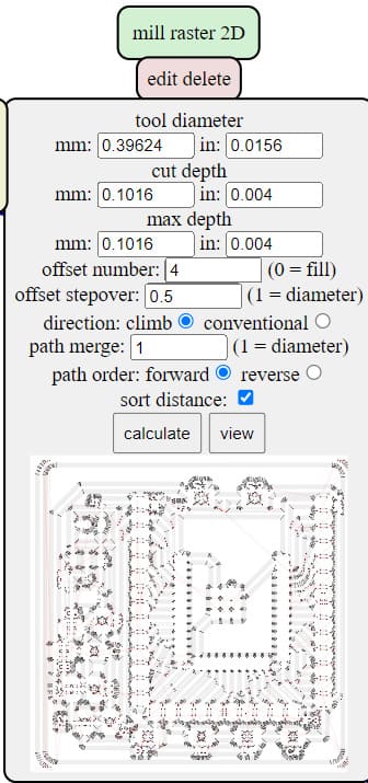
So, now that we can use mods, let check how well it went for my circuit. Spoiler alert: It took me a while to finally get it right. It's just a matter of keep going.
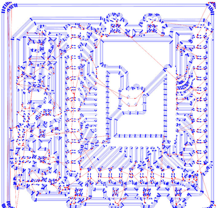
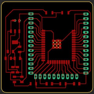
Attempts
The errors will be pointed with a purple box.
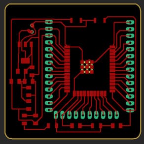
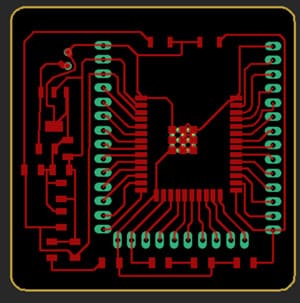
First Attempt:
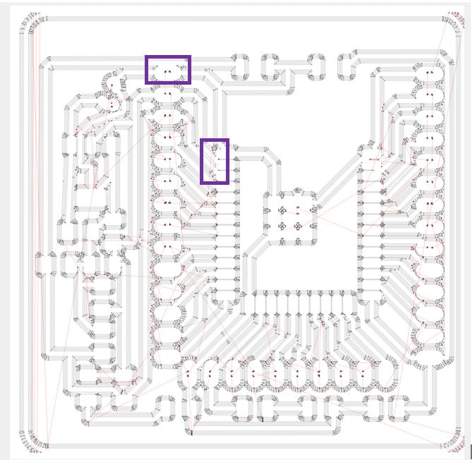
Second Attempt:
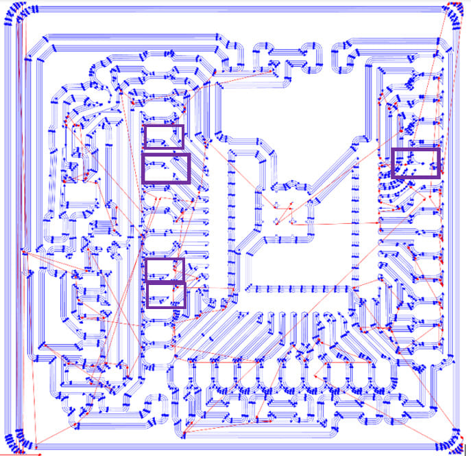
Third Attempt:
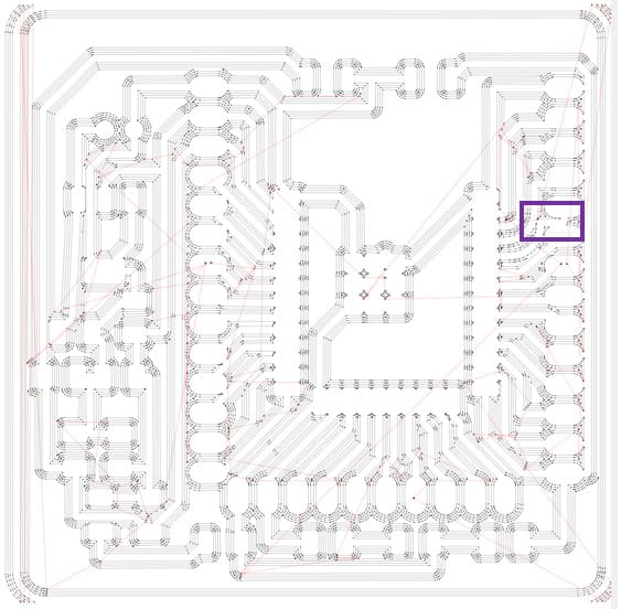
Fourth Attempt:
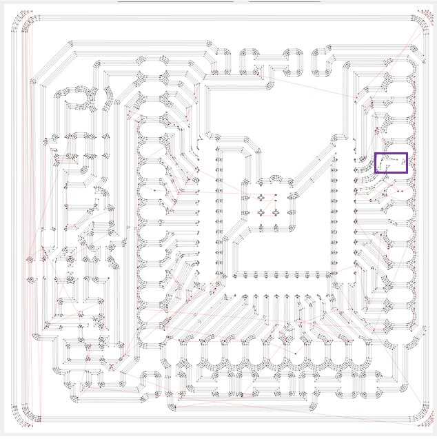
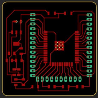
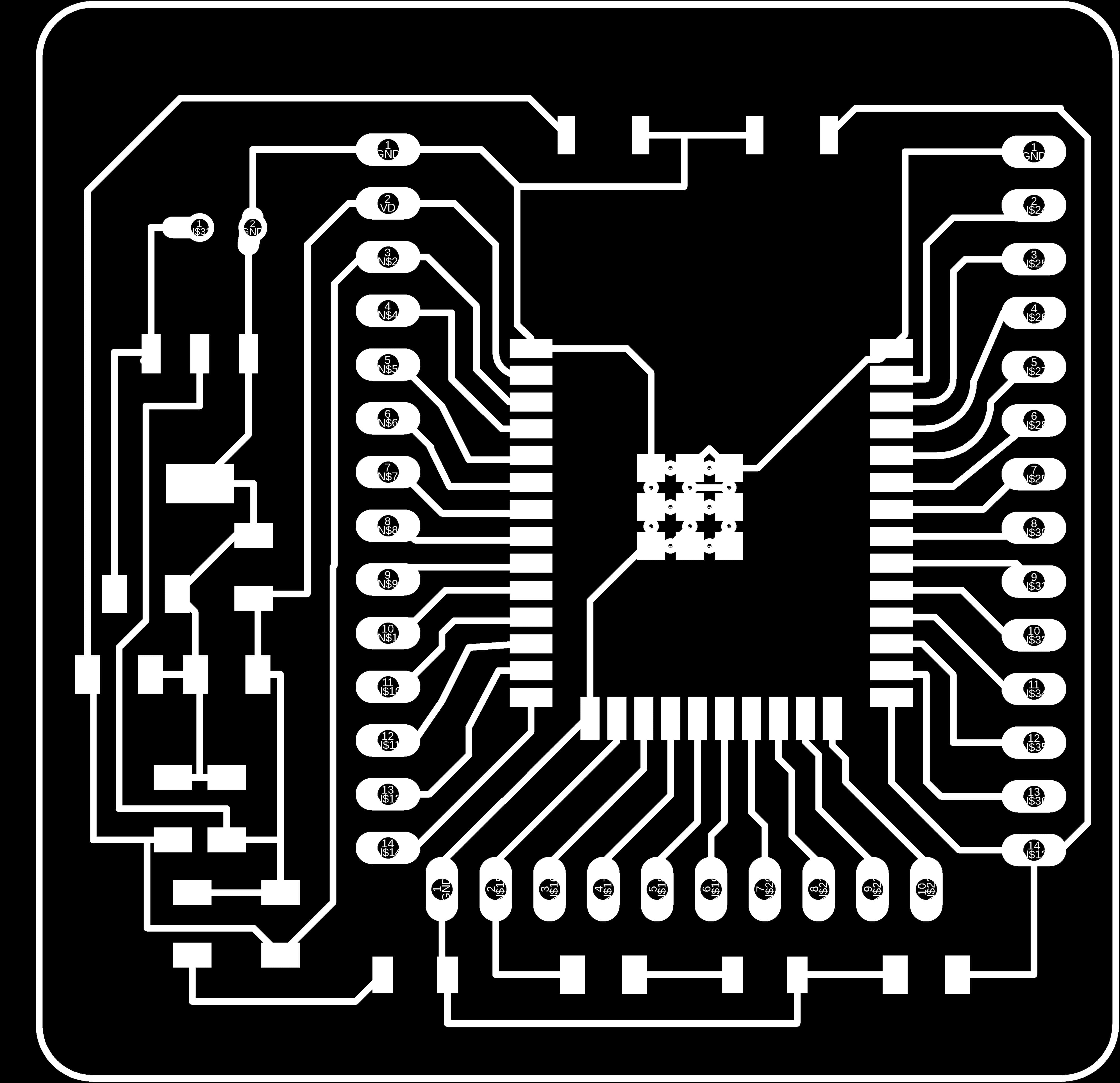
Fifth Attempt:
The fifth attempt didn't have shortcut problems, so I'm staying with this one.
See the following gallery to compare the changes the electronic design went over each attempt!


Cutting the circuit
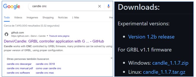
Now that we have our file ready, let's go to Candle. *If you haven't download Candle, search in the web, it was easier for me to find it searching for “candle cnc”. Go to the github page and download the GBRL zip file.*
Now, execute Candle and open your .nc file.
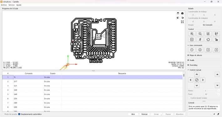
This is a preview of the circuit in candle.

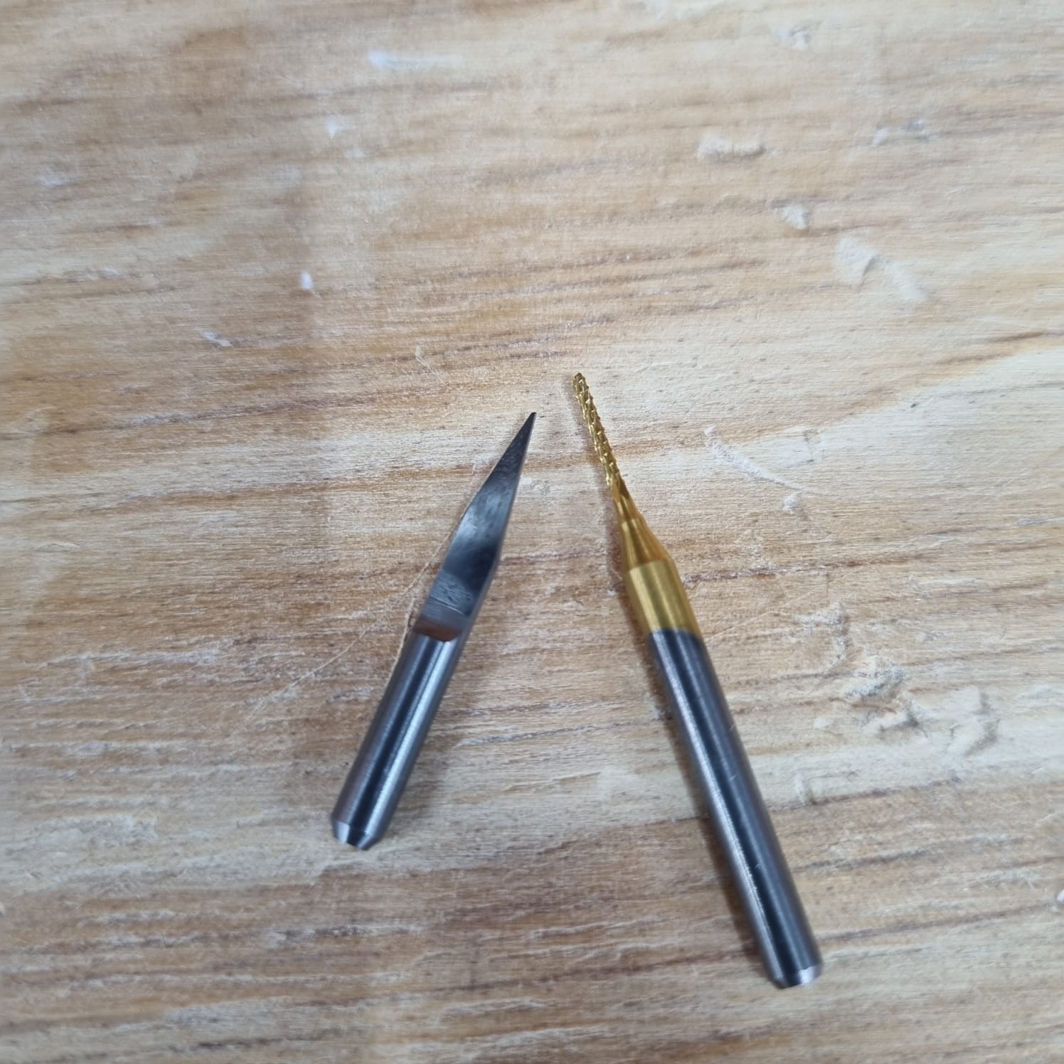
So now, we are ready to cut. I'm using a V-Groove mill to trace the routes and a 1/32" ball nose end mill for the contour.
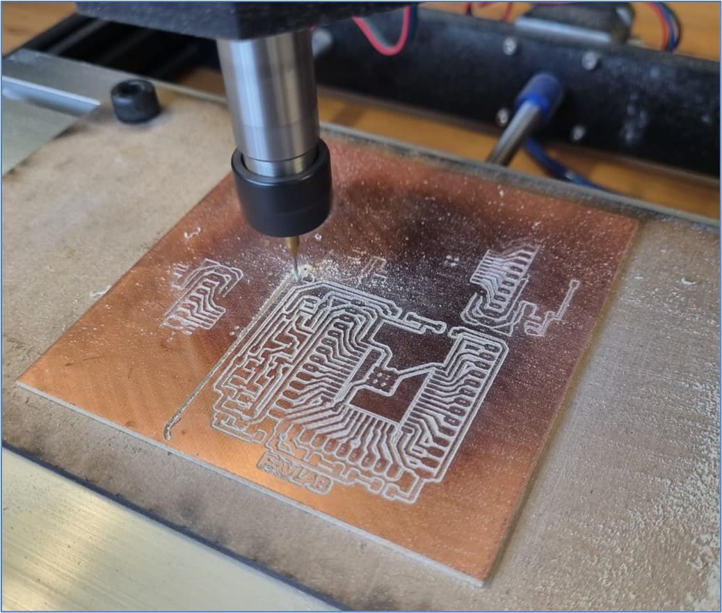
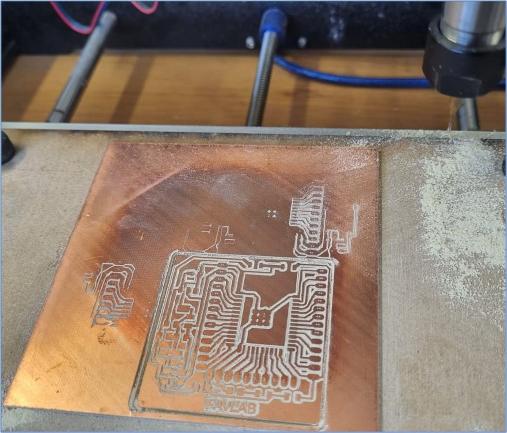
Machining process:
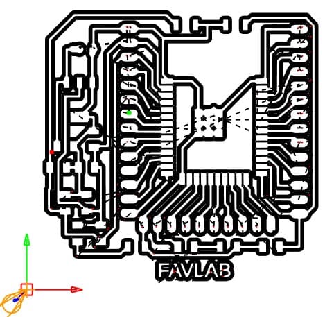
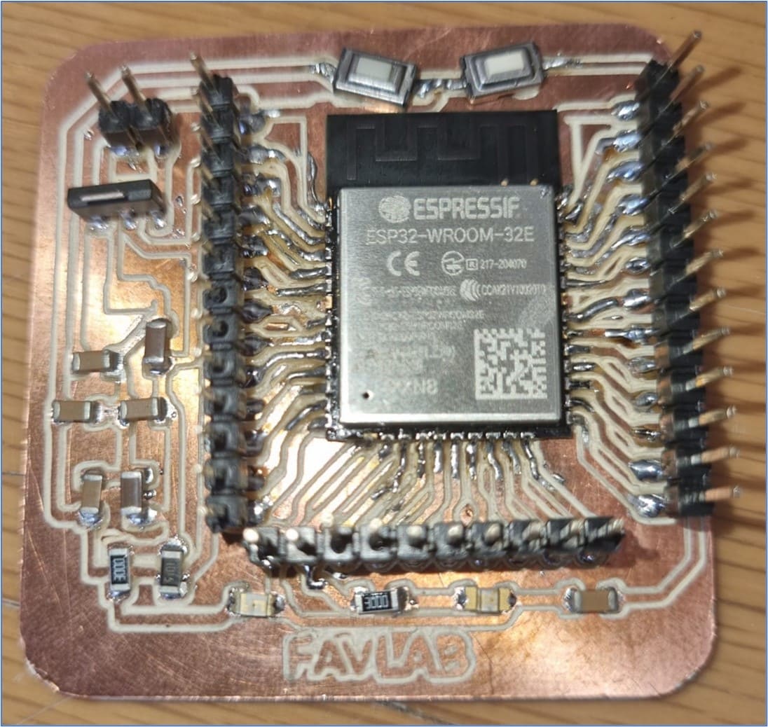
And here we finally have our circuit PCB:
Soldering time!
After many attempts to get the PCB, it's time to solder the components. This was not easy, the components were so small and the PCB I designed was to compact, because I wanted it to look “pro”…
It took many attempts again. I even ruined one esp32.
But this is me, making it look like if I knew what I was doing…
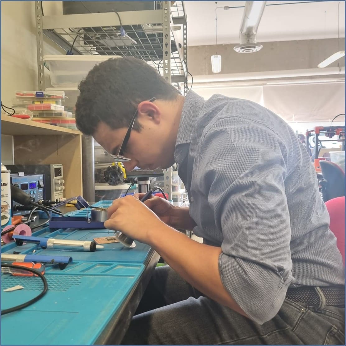
I repeat, after many attempts, I finally got it, my circuit.
Soldering time!
Searching for the correct temperature to solder our circuit I asked different electronic blogs like Techspray and buil-electronic-circuits. The suggested temperature range goes from 320-370°C, so I decided to use 350°C as my soldering temperature.
After this, I deserve a break, right? Wrong! That doesn't exist in Fab Academy. (Sad Face☹)
The time of the truth
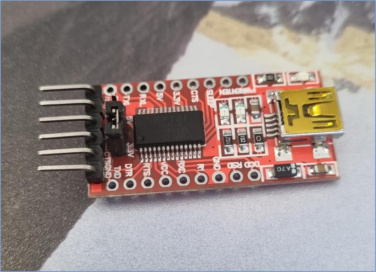
Ok, so now that we have our PCB, let's program it! I didn't designed the PCB with a port to download a program, instead, I will use serial communication to do so. I'm the module YP-05 FTDI FT232L USB to TTL UART.
Then we connected the module, the circuit, and my computer.
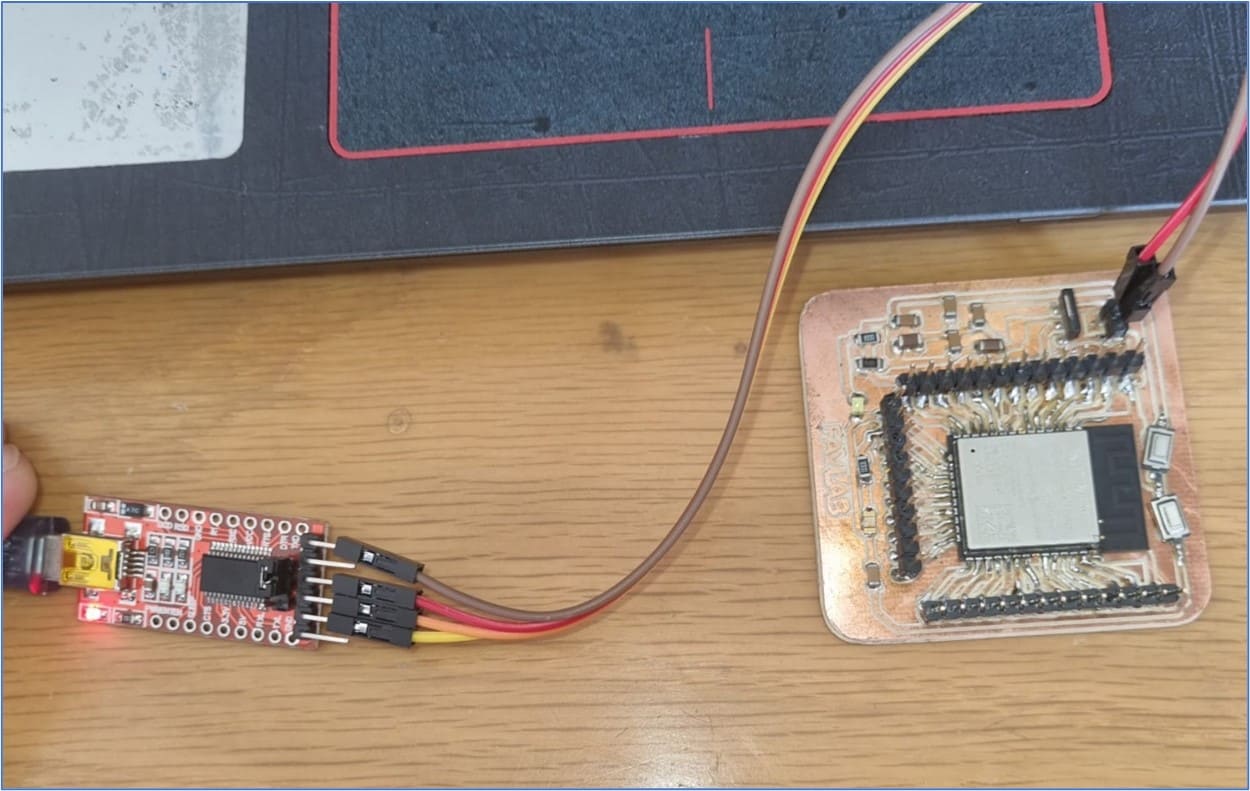
I'm going to download the blinking led program, and here you have it. My circuit is alive! Feeling like Frankenstein jaja…
After this, I deserve a break, right? Wrong! That doesn't exist in Fab Academy. (Sad Face☹)
Here, you can download the board files: