
Grupal Assignment.
Use the test equipment in your lab to observe the operation of a microcontroller circuit board.
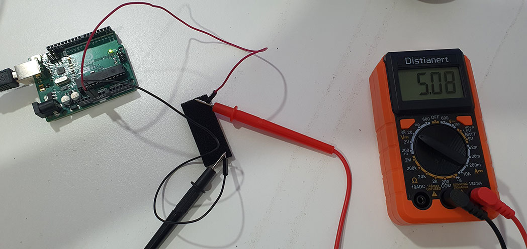
We tested the voltage on the pins to check if they matched the value printed
First test with the 5V Arduino Uno R3 pin.
Then with the 3.3V pin
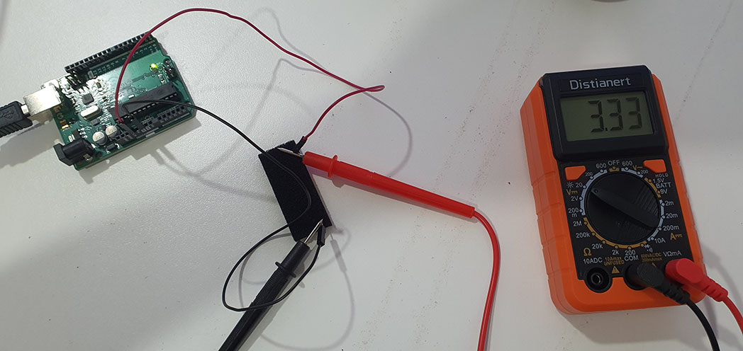
In both cases the voltage was correct.
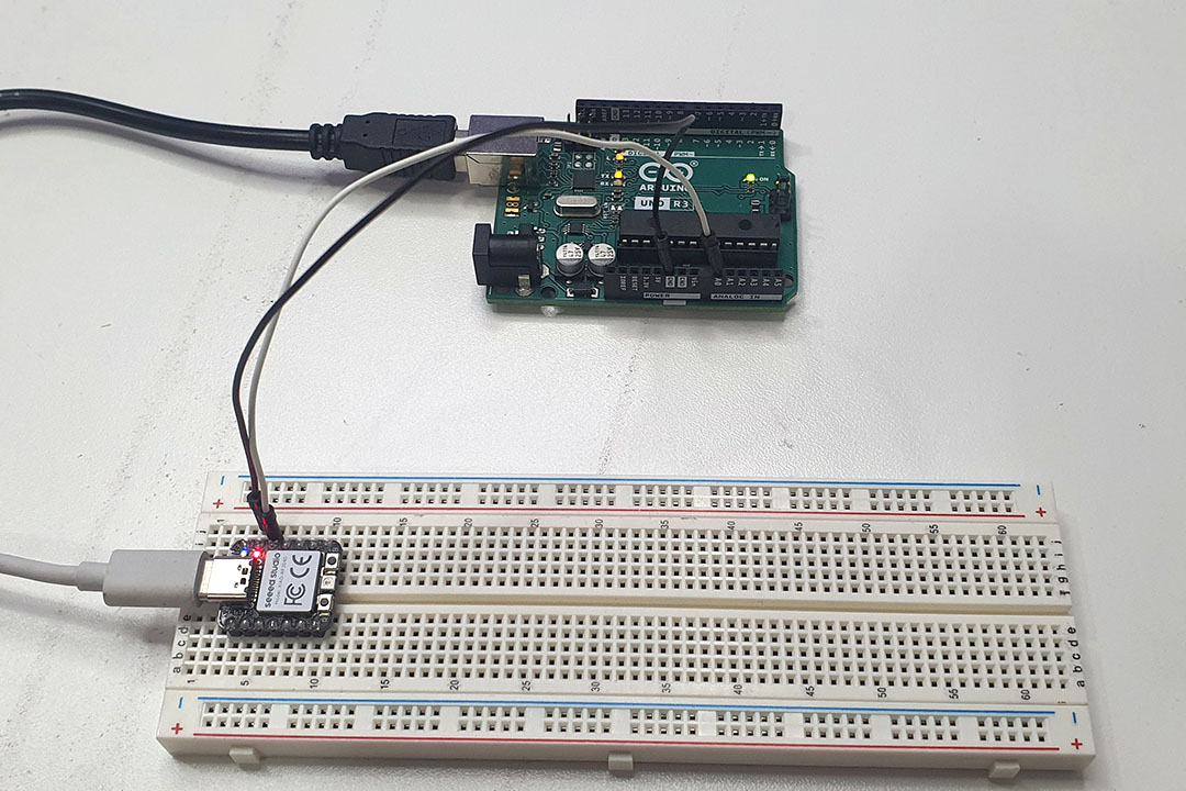
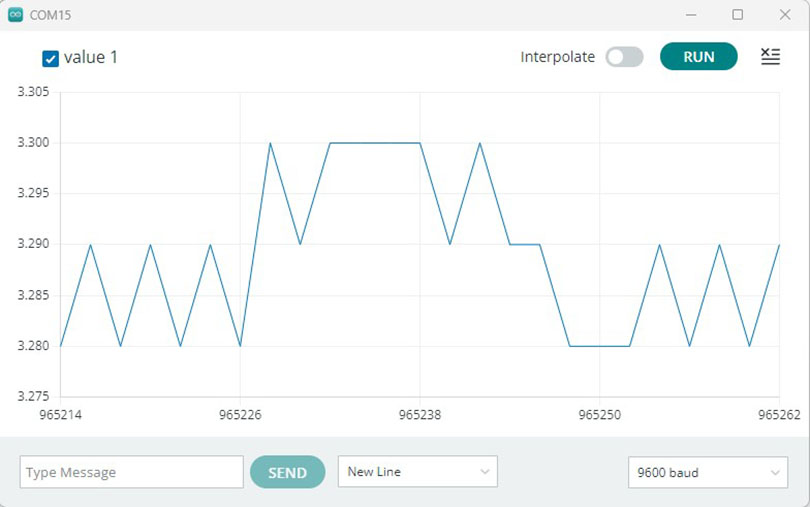
I did not have an Oscilloscope so I decided to make my own.
I followed this tutorial.
I wanted to test the 3.3 voltage of the Xiao RP2040.
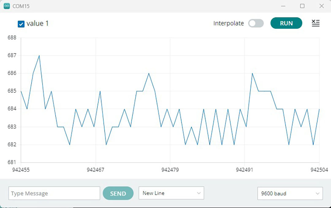
The values weren't accurate, so I modified the code to have the values in volts.
The value goes from 682 to 687, the average is 684.5, divided by the 3.3V it gives a 207.42 factor
I just divided the value by the factor to have a value near reality.
I also added a delay so the curve won't move so quickly.
        Here is the final code:

           void setup() {
           Serial.begin(9600);
           }

           void loop() {
           float val = analogRead(A0);
           Serial.println("Voltage:");
           Serial.println(val/207.42);
           }
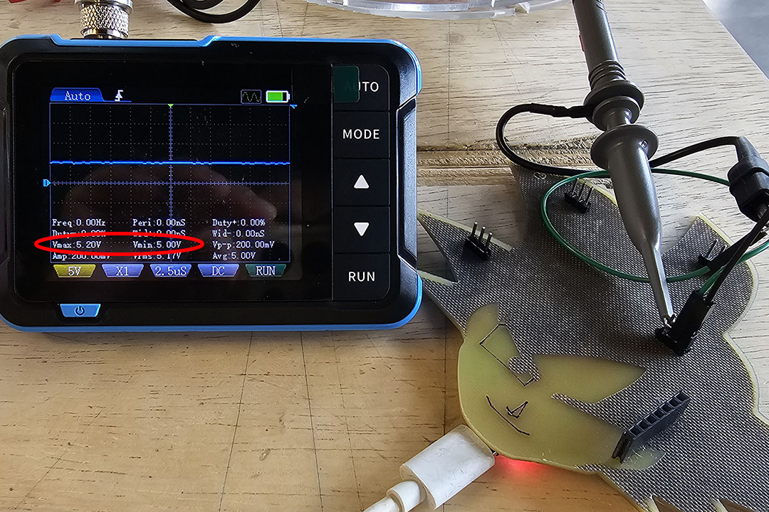
After we bought this Oscilloscope, we run some tests on the Goku PCB Board.
We connected the gray probe to the 5V pin on the Xiao and the black pinch on the ground pin of the Xiao.
It gave the 5.0V - 5.2V reading as shown on the picture.
Individual Assignment.
Use an EDA tool to design a development board that uses parts from the inventory to interact and communicate
with an embedded microcontroller.
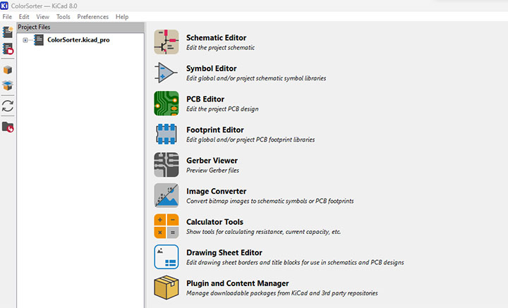
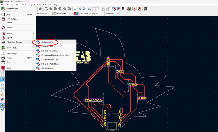
For this assignment I used KiCad 8.0
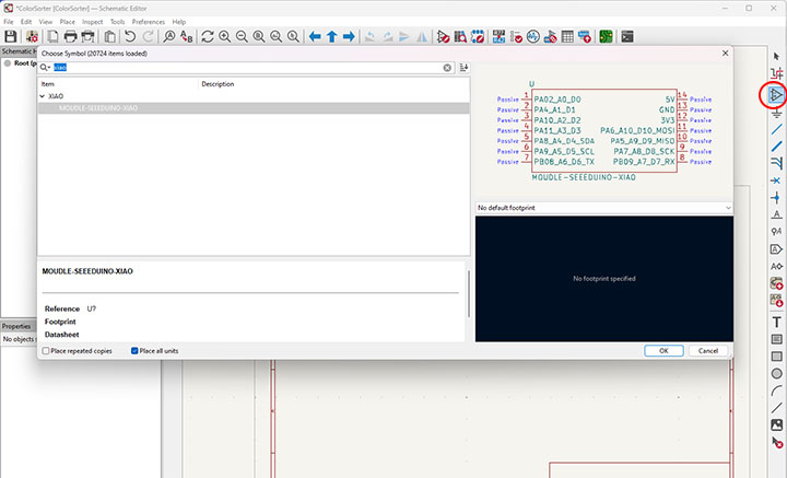
After installing KiCad, I also installed the symbol and footprint for the Xiao RP2040 microcontroller found here.
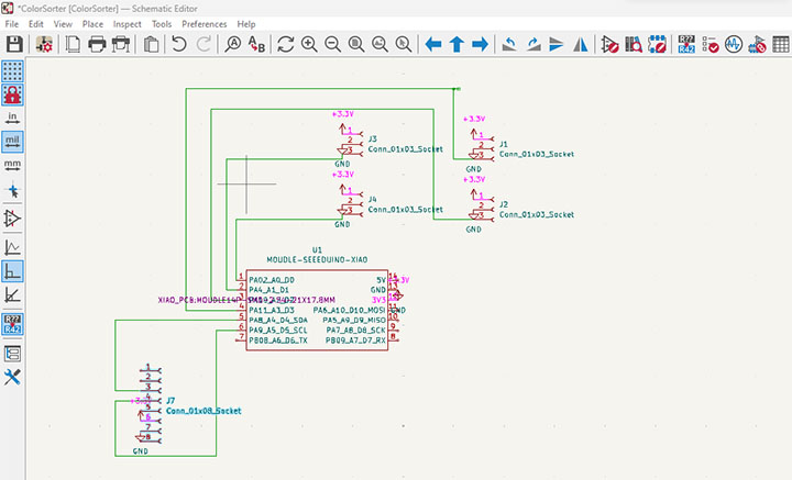
First we start with the Schematic Editor and add components with the Add a symbol icon o the A key.
In the same way I added several connectors and then added the wires for the connections.
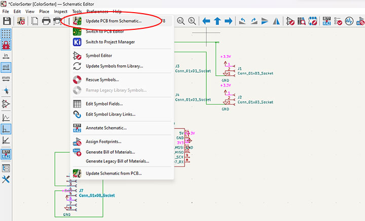
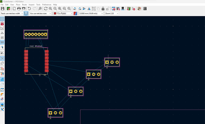
I updated the PCB from Schematic.
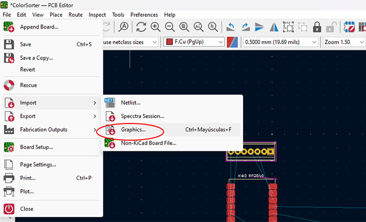
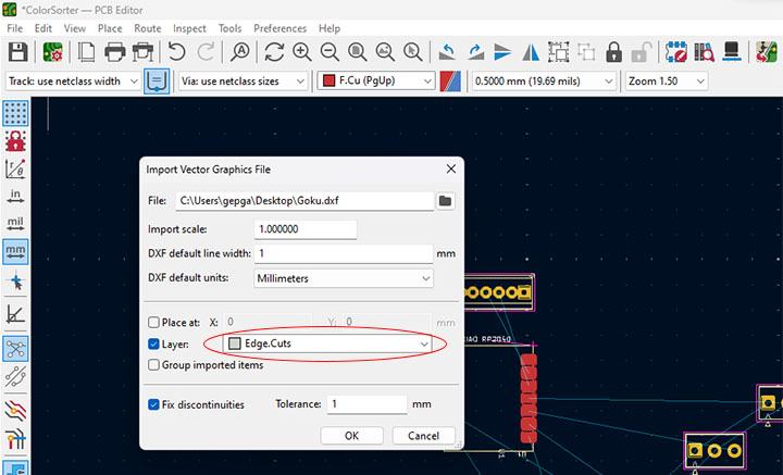
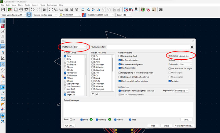
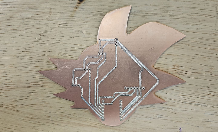
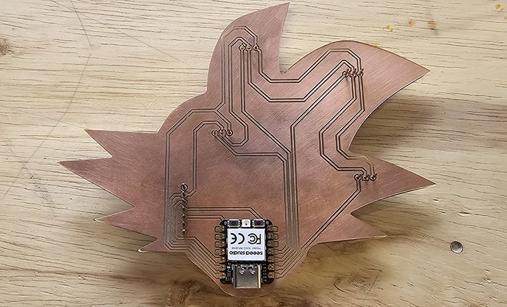
Then I added a shape for the PCB in the Edges Cuts layer. As a tribute to the late Akira Toriyama,
I chosed the head of Son Goku.
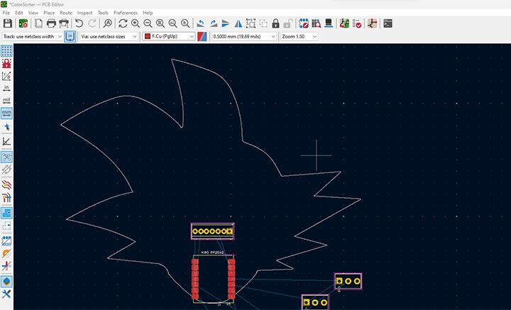
Then I had to create the pathway for the connections which was a real puzzle. I used 0.8mm for power and GND path and 0.4mm for connections.
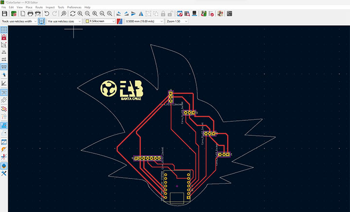
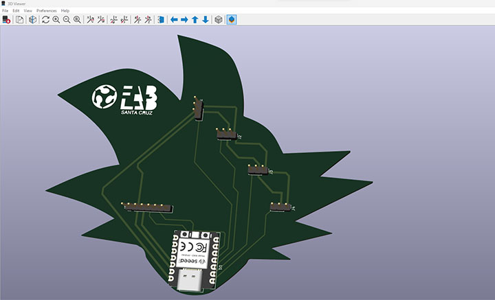
The 3D view.
Then I exported as DXF the files to Aspire.
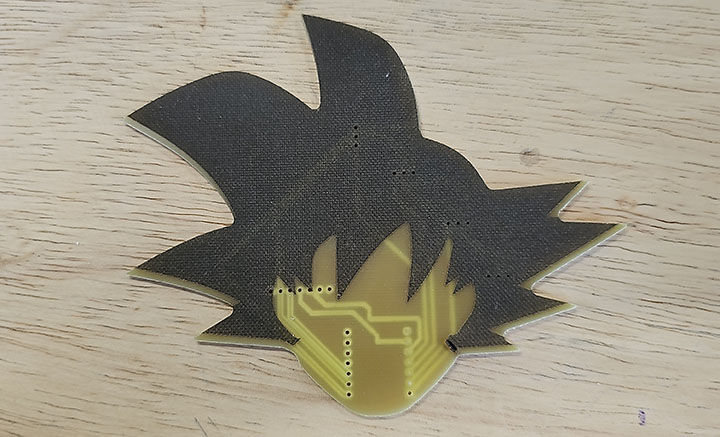
First I tried my DXF files on the laser cutter on MDF to see if there is some troubles before sending it to the cnc
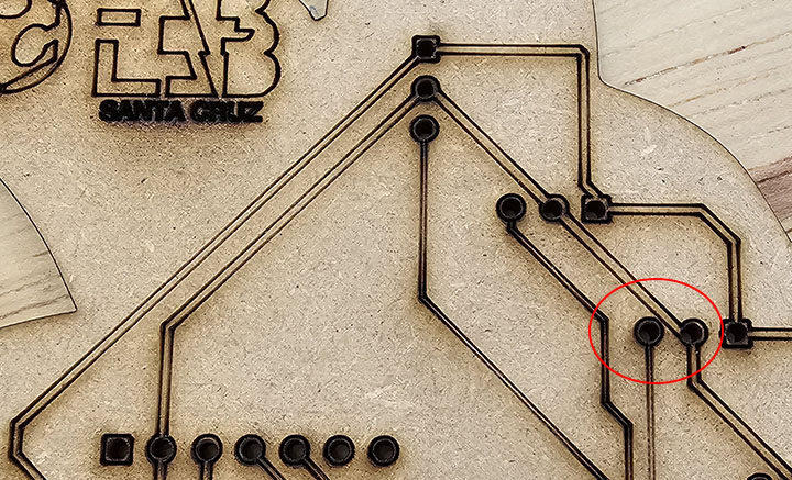
Here the paths are together so I changed.
First try with the CNC with a 10 degrees flat tool. I went too deep, 0.25mm instead of 0.035mm.
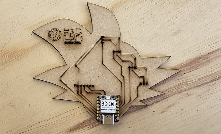
The laser part went well.
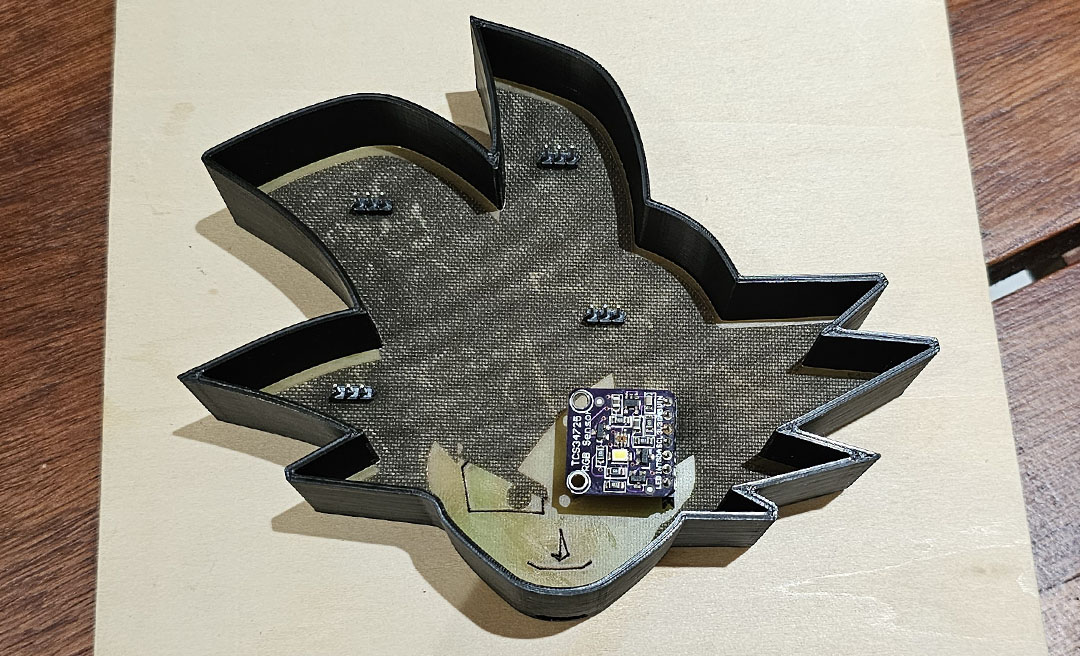
I'm making the new PCB to correct de paths and making a case for it.
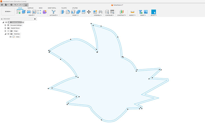
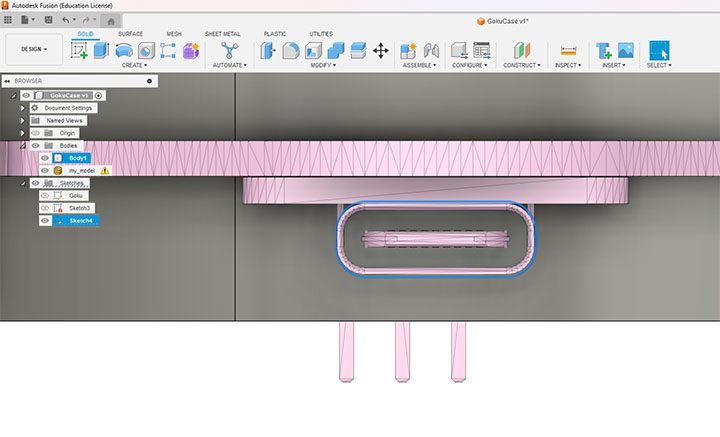
I will use Fusion to make the case, first I imported the shape.
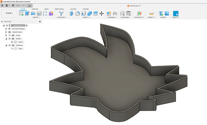
Then I extruded to have a 3D model.
I imported the 3D Model from KiCad so I can make the holes for the connexions.
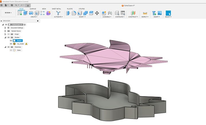
I moved the PCB Model so I could make the holes by copying the shpae of the connexions.
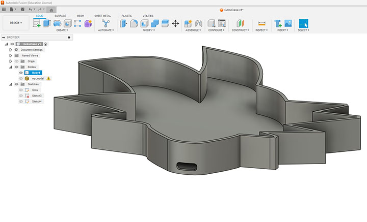
You can download the case here
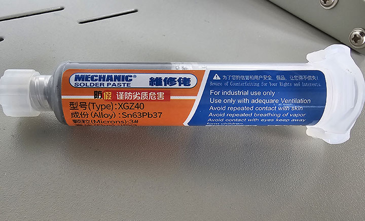
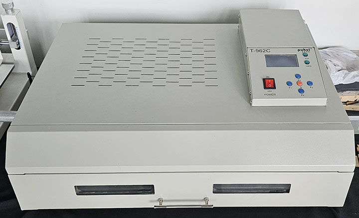
For the new PCB, I used Soldering Paste and an InfraRed Oven.
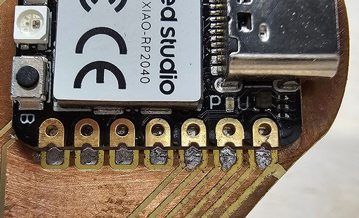
Here is the result.
Here are the files to be downloaded.
extra credit: try another design workflowextra credit: make a case for it
extra credit: simulate its operation