
This week's assignment is to make a 2D design for production using a CNC machine.
The machine that we will use for this assignment is the Roland Modela MDX-20 Milling Machine, the most relevant aspects are the following:

Figure N°1
| Max. operation area | : 203.2 mm (X) x 152.4 mm (Y) x 60.5 mm (Z) |
| Interface | : Serial (RS-232C) |
| Tool chuck | : 6 mm or 1/8 in |
| Spindle motor | : 10W (DC motor) |
| Revolution speed | : 6500 rpm |
| Acceptable material | : Wood, Plaster, Resin (modeling wax, styrenform), Chemical wood |
The user manual for this machine can be found here.
To be able to establish the zero point in Z, you must have both the milling cutter and the plate in place and go raising or lowering the milling machine with the buttons of the machine until it wears out a bit of the material.
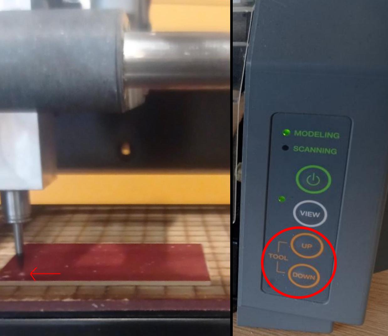
Figure N°1
In order to know what the limits of the milling machine that we use are, we have the file with the design rules, with this we have the different track widths.
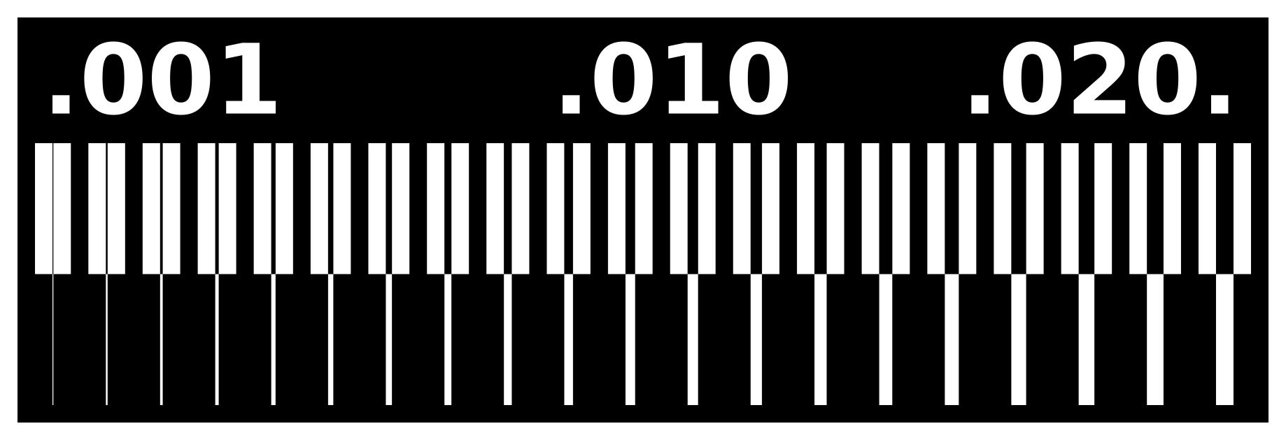
Figure N°2
We use mods projects to be able to generate the layout files taking into account the DPI of the file and the width of the cutter, which is 1/64'' in diameter.
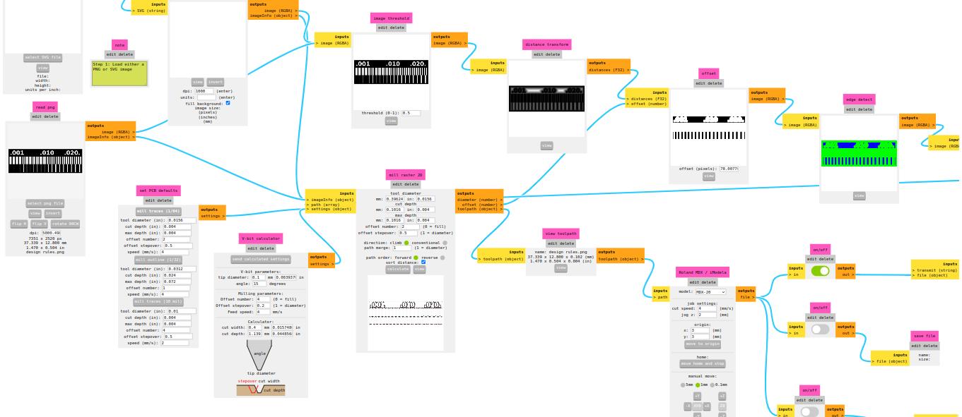
Figure N°3
We see that the traces were generated correctly.
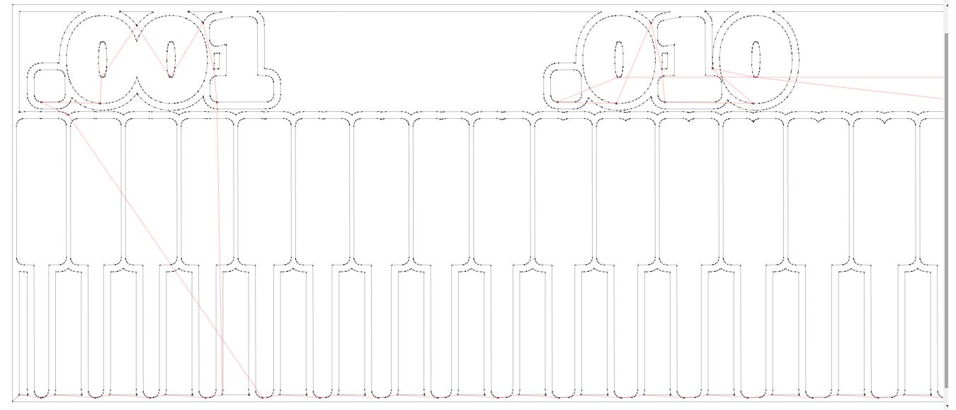
Figure N°4
We have the result where it is observed that track widths could not be achieved.

Figure N°5
If we zoom in we observe the minimum track width that we can make is 0.08'' or 0.2mm
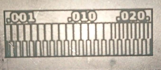
Figure N°6
For the creation of the PCB we will use the design made with KiCAD in week 06, it has an ATtiny44 as its central unit and is programmed via ISP.
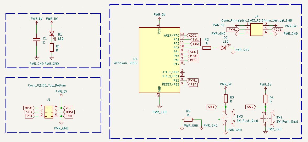
Figure N°7
Plus it has a Grogu-shaped outline.
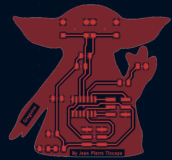
Figure N°8
From KiCAD we export in SVG format the vectors corresponding to the tracks, the contour and the mask.
The flow from ModsProjects would be the following: Open Program --> Roland --> MDX Mill --> PCB
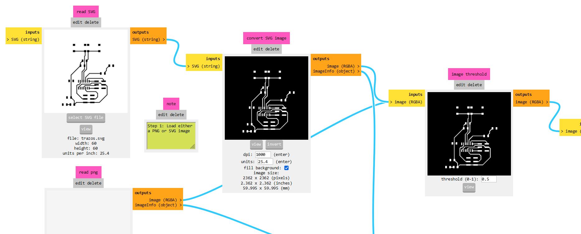
Figure N°9
For this job we will use a 1/64 bit so we select "mill traces (1/64)" and then calculate the path.
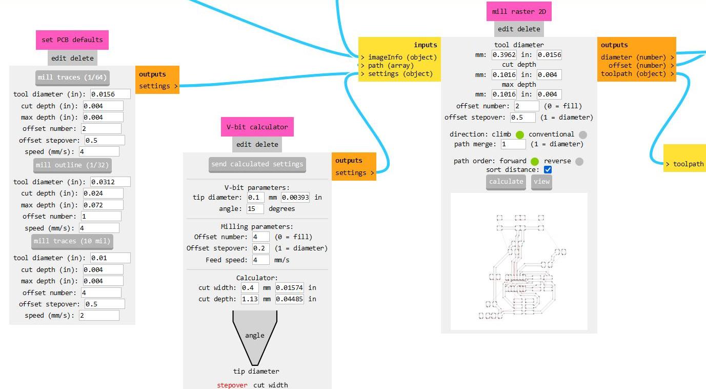
Figure N°10
We see the path traced correctly.
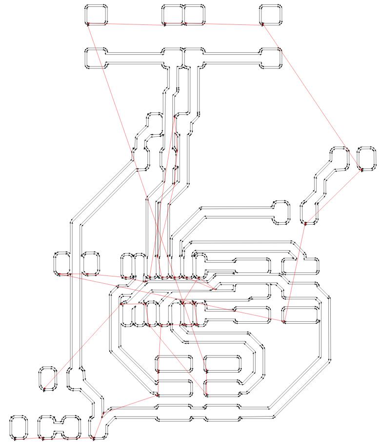
Figure N°11
In the same way, to cut the plate, we import the SVG file of the outline, we change the DPI to 1000 and we invert the image, the difference is that now we select "mill outline (1/32)" since this is a drill of cut and with a different diameter.

Figure N°12
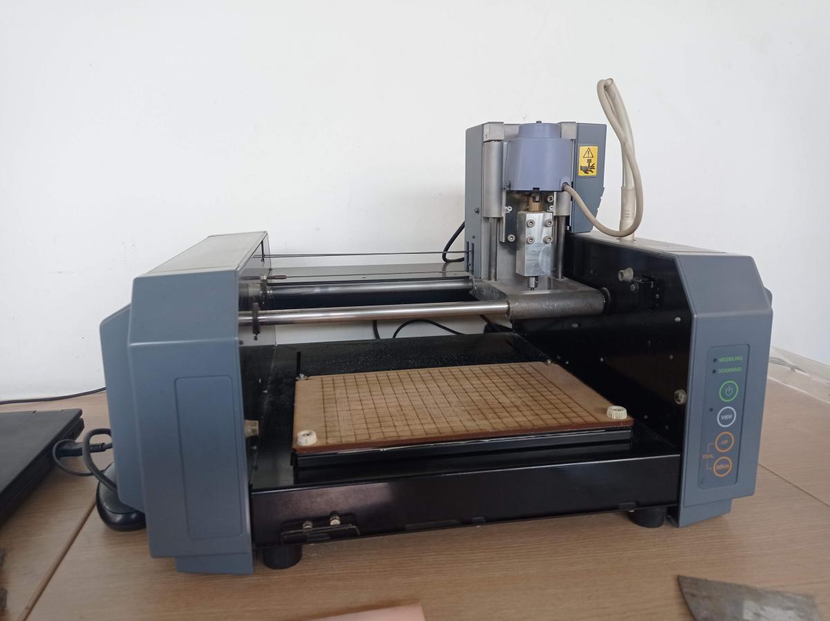
Figure N°13
In order to start manufacturing, we will use a copper plate that was previously cleaned with isopropyl alcohol.
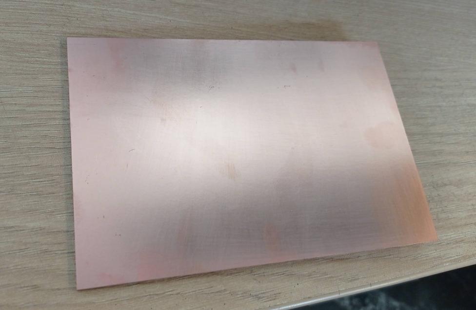
Figure N°14
We added double-sided tape to the back of the copper plate.
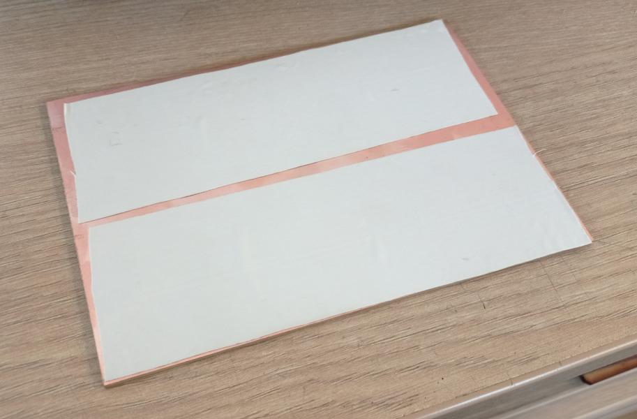
Figure N°15
We stick this plate firmly inside the grid since they indicate the position in coordinates. Then the height of the drill must be calibrated so that the 0 point coincides with the plate.
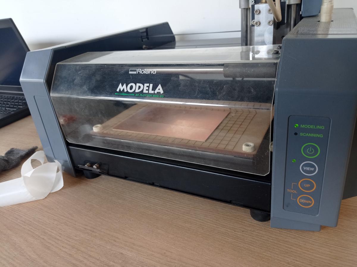
Figure N°16
We cover the machine, we send the generated file through the ModsProject and it starts to trace.
Video N°1
We also see that the obtained result is satisfactory.
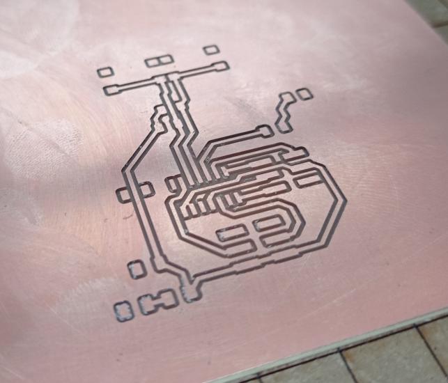
Figure N°17
We change the drill for the cutting one and repeat the calibration process, later we send the cutting file to the machine.
Video N°2
We also see that the obtained result is satisfactory.
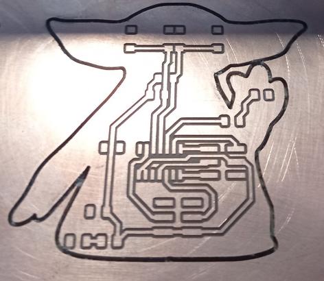
Figure N°18
We carefully remove the PCB and remove the outer part of the board.

Figure N°19
To apply the soldering mask it is advisable to wear gloves and have it on a surface that we are going to discard since the paint can come out on the sides.
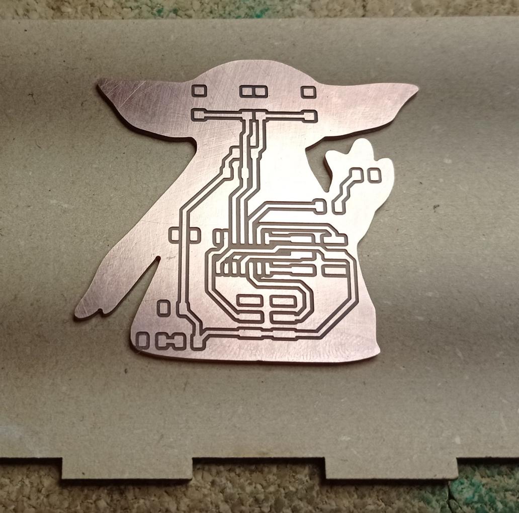
Figure N°20
The solder mask that we will use is a Mechanic 10ML GY-UVH900 in green color, this can be purchased on Amazon.
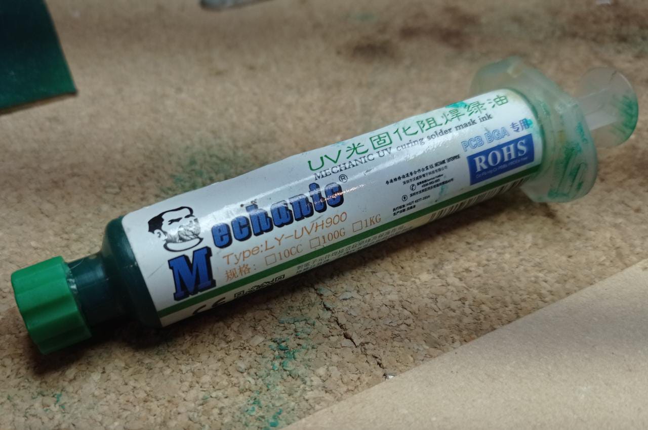
Figure N°21
We apply the paint from different points and we extend it with a brush.

Figure N°22
In order to dry this anti-solder mask you need to use UV light, in our laboratory we have a curing machine for the 3D resin printer, here we place the PCB for 10 minutes.

Figure N°23
To remove the mask of the pins that must be soldered we will use a wear based on an engraving with the laser cutter. For this, a power test was previously carried out on a plate with an anti-solder mask.
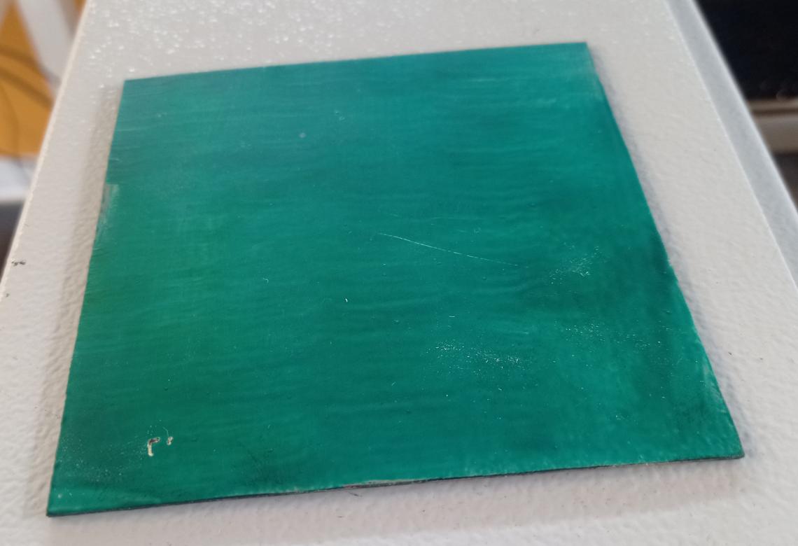
Figure N°24
We see in the image the power percentage from 0 to 100%, the conclusion was that 80% power was the appropriate value to remove it from the board.

Figure N°25
Inside an MDF plate, an outline of the plate was cut to later place our PCB with the already cured mask in the same position.
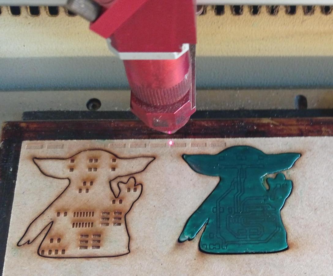
Figure N°26
Here we import the SVG file created in KiCAD corresponding to the mask and we send instructions to the cutter to work at 80% of its power.
Video N°3
We see a good result but with certain corners that were not completely worn, this may be because the expansion of the mask was not completely homogeneous and a second or third pass with the laser cutter was needed.

Figure N°27
To make the soldering of this PCB easier, a flux syringe was used.
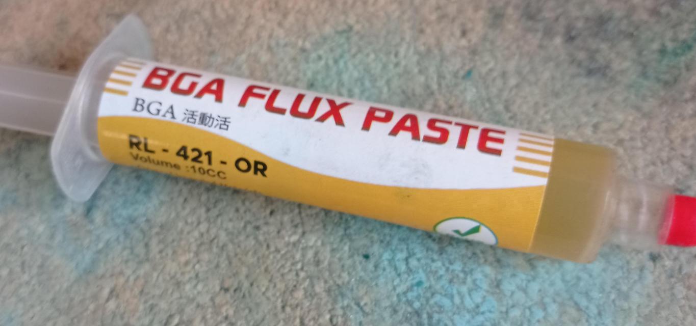
Figure N°28
This is how the plate looks with the flux applied and dried.
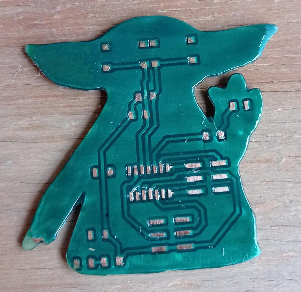
Figure N°29
The components are soldered.
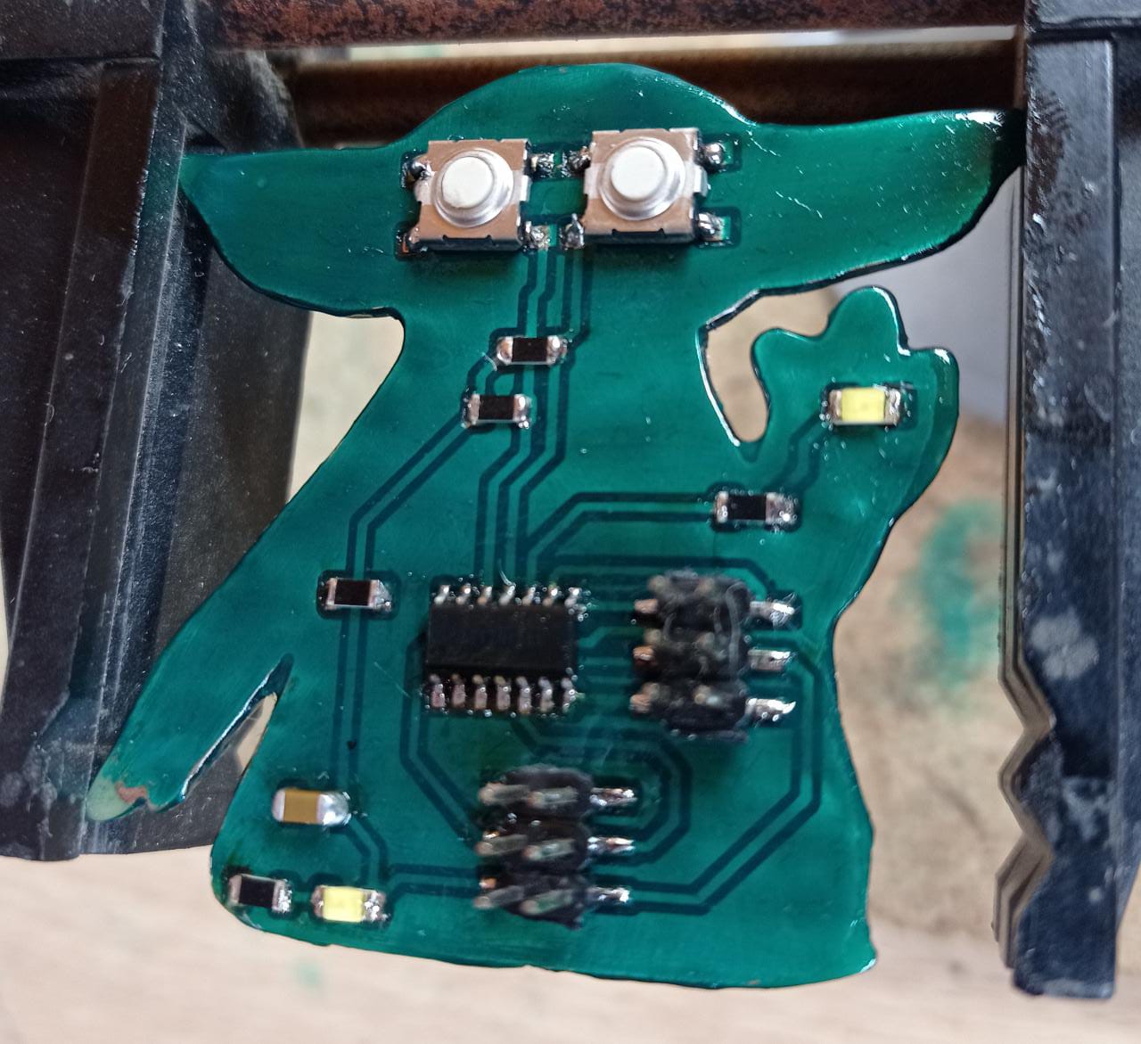
Figure N°30
And this would be the final result with the shell designed in week 06 that forms Grogu's clothing.
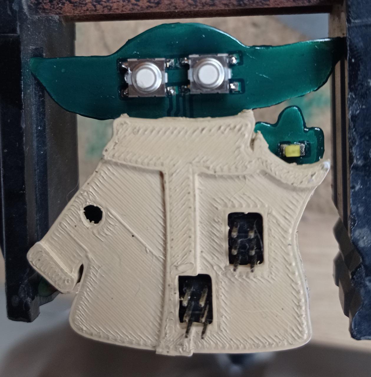
Figure N°31
Having the board ready, we proceed to program it with the classic Arduino "Hello World", that is, a Blink, for this we will use the USBAsp programmer that connects via ISP protocol.
Video N°4
Finally we created a simple script to quickly turn on the led by squeezing one of Grogu's eyes.
                      void setup() {
                        pinMode(1,INPUT);
                        pinMode(3,OUTPUT);
                        }

                        void loop() {
                        if(digitalRead(1)==LOW){
                          digitalWrite(3,HIGH);
                          delay(100);
                          digitalWrite(3,LOW);
                          delay(100);
                          }
                        else{
                          digitalWrite(3,LOW);
                          }
                        }
Grogu is alive!
Video N°5
The files created or used this week can be downloaded here:
| Grogu PCB - Design in KiCAD | Link |
| Grogu PCB - traces | Link |
| Grogu PCB - outline | Link |
| Grogu PCB - mask | Link |
| Simple Grogu Script | Link |