
This assignments's homework is to use the lab equipment to test one of the microcontroller boards.
In the first test we will use a Groove Seed Studio module with the XIAO RP2040 module with a potentiometer to read an analog value, transform it to voltage and print it on the serial monitor.
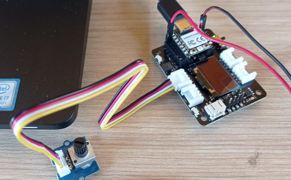
Figure N°1
Simultaneously we will use a multimeter in voltmeter mode to verify that the voltage value obtained matches reality.
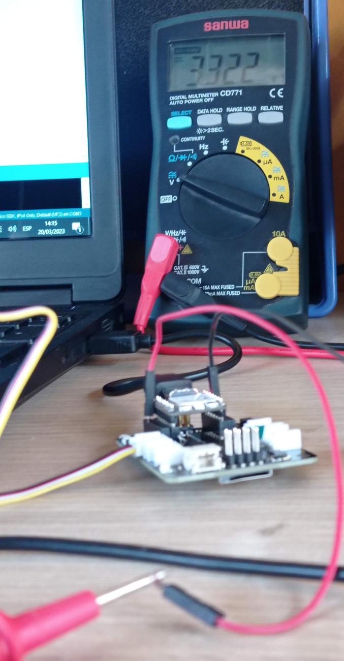
Figure N°2
We see in the video that the values read are almost identical to those read by the multimeter.
Video N°1
In the second test we will use an arduino uno module with a potentiometer, in this case we will generate a square pulse width modulation (PWM) pulse.

Figure N°3
This pin will be read directly with a channel of the oscioscope to observe how the duty cycle varies from 0 to 100%.
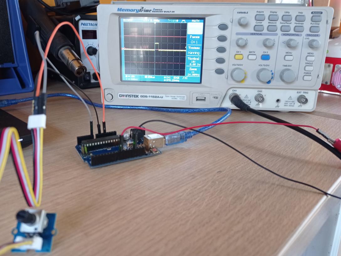
Figure N°4
We see in the video that the pulse is correctly graphed based on the value of the potentiometer.
Video N°2
This week's individual assignment was to do an electronic design. For this, the chosen software was Kicad in its version 7.0.
In the main menu we have the different editor options for schemes, plates, symbols and footprints.

Figure N°1
The first step is to create a project and within it have a schematic (in .kicad_sch format) and a board (in .kicad_pcb format).

Figure N°2
In the initial schematic window we configure the default global footprint table.

Figure N°3
The first step to make our scheme is to add components, we can do it with the shortcut "A" and it will load the list of components.
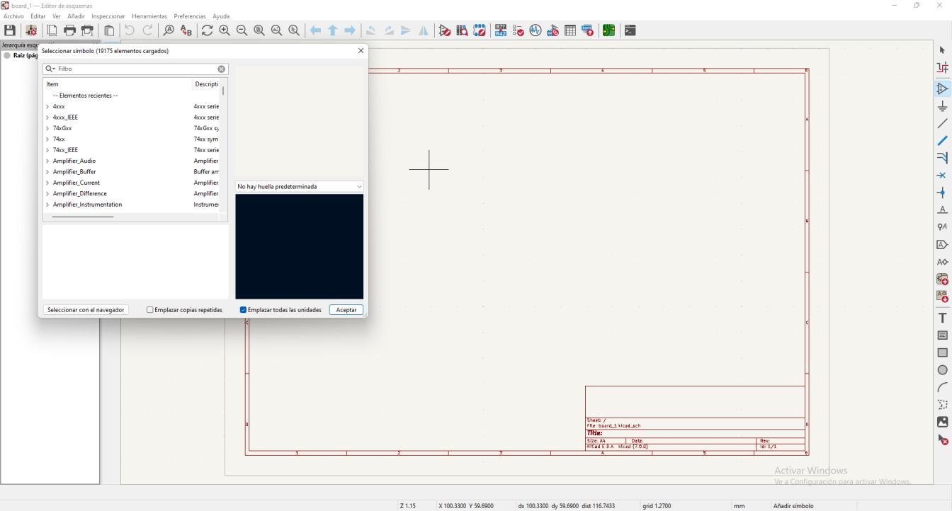
Figure N°4
We start by adding the microcontroller that will be the Attiny44.

Figure N°5
We do the same with a generic resistor.

Figure N°6
We are looking for a ceramic capacitor (no polarity).
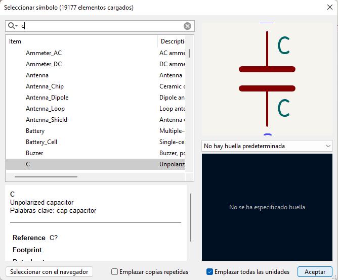
Figure N°7
Then we add a 4-pin pushbutton.

Figure N°8
The microcontroller that we will use is programmed through the ISP protocol which uses 6 pins, so we will add a 2x3 connector.
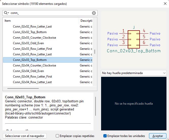
Figure N°9
One of the best ways to make connections neater is to use labels.

Figure N°10
With that the connections for the programmer will be made easier.
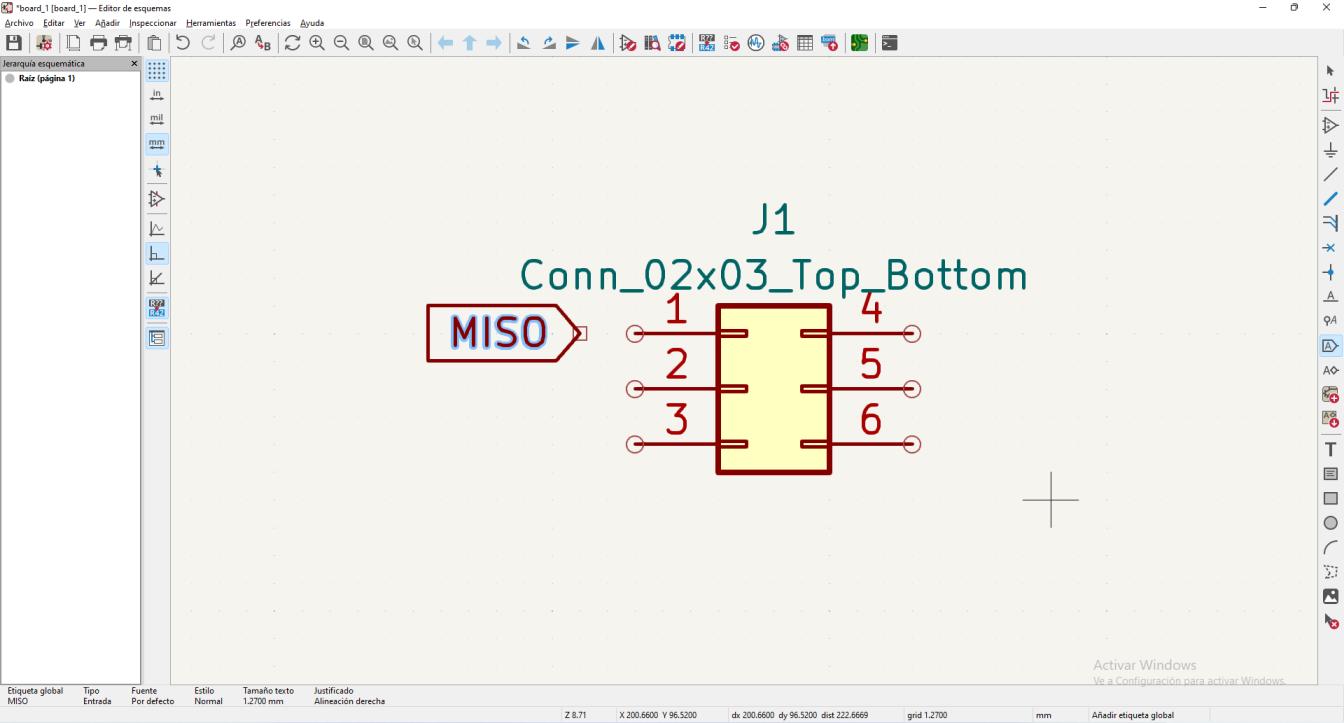
Figure N°11
We complete the pins for the ISP (MISO, MOSI, SCK, RESET, VCC, GND).
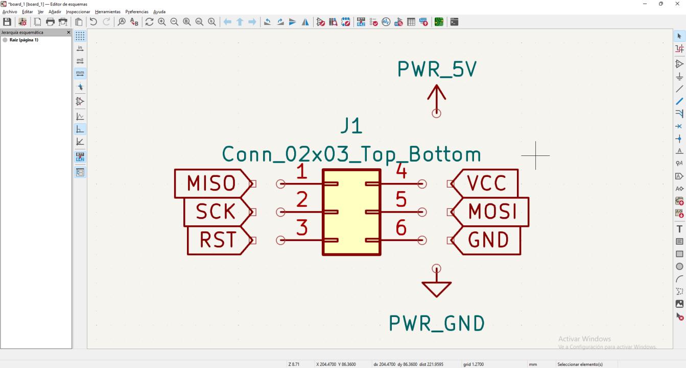
Figure N°12
We can see the entire ISP section completed in Figure No. 13

Figure N°13
We add rectangles to separate the sections of the design and we have the complete design.
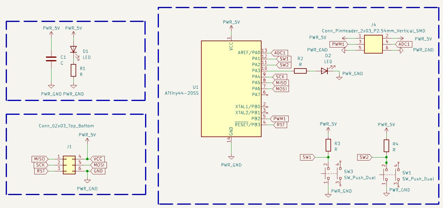
Figure N°14
The next step is to assign each symbol a fingerprint that is the way it will be represented on the plate.
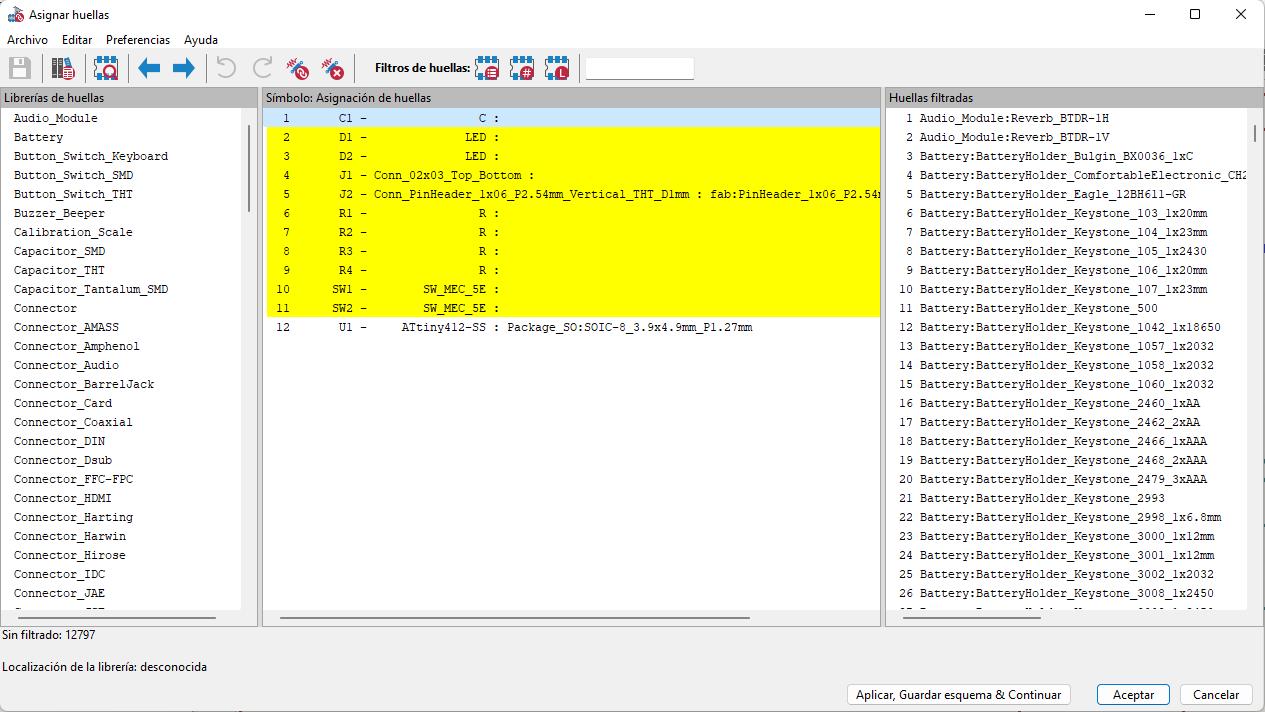
Figure N°15
When we have difficulty finding the right footprint, we can look closely at each of its parts.

Figure N°16
Within the footprint we can measure the sections with the ruler tool to be able to confirm that it corresponds to the component that we physically have.
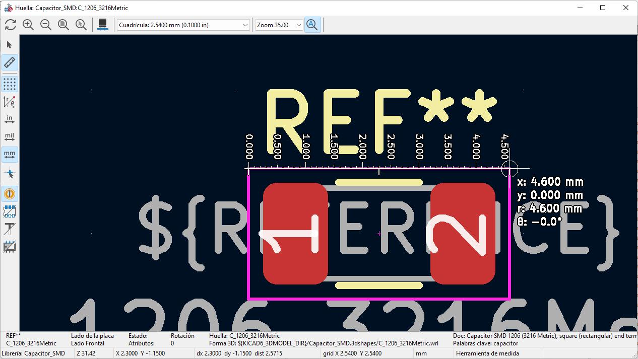
Figure N°17
When the fingerprinting is complete we go to the edition of the board, using the update from the schematic.
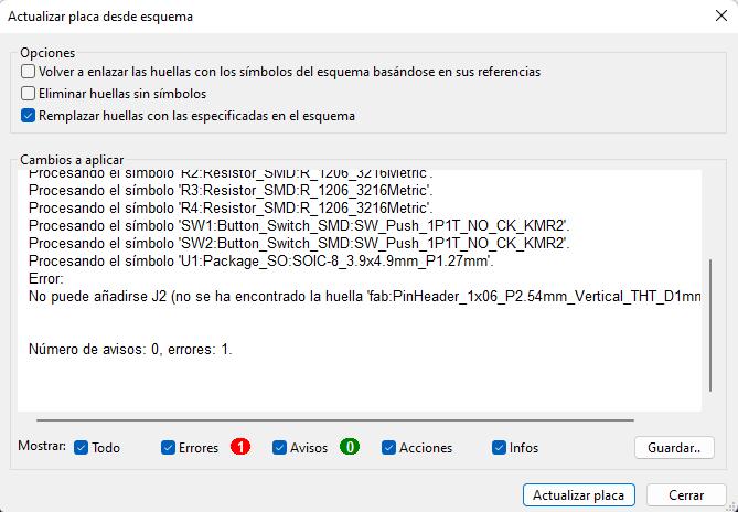
Figure N°18
Updating adds the components to the scene.

Figure N°19
We are going to vary the classic design of a square for the PCB and changed it for a more friendly design. We will use baby yoda (Grogu) as a reference to create the design of our plate, taking advantage of the fact that it is green and we can add anti-solder mask to make it more similar.
We will use a reference image where he is raising his hand (like using force)
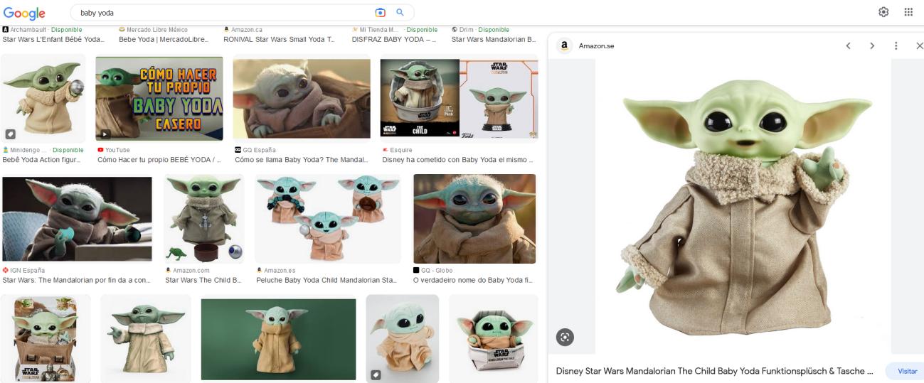
Figure N°20
We import this image into Blender, here we can use it as a reference to outline the image through points.

Figure N°21
We complete the entire contour by extracting each point and closing the end with the shortcut F.

Figure N°22
With the surface subdivision tool we can make this section rounded.

Figure N°23
We see the outline of the image in Figure No.24

Figure N°24
Within Blender we see that the contour was modeled correctly and can be exported in .DXF format.
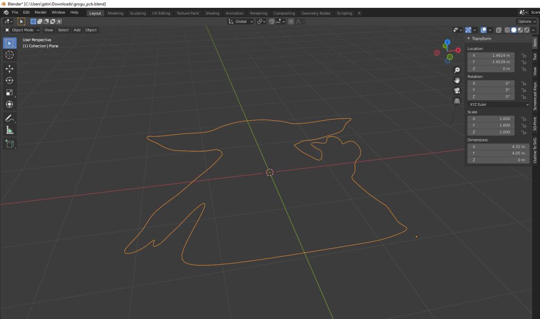
Figure N°25
Now inside Kicad we are going to import the generated contour.
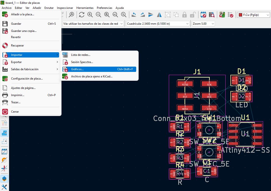
Figure N°26
It is necessary to choose that this outline belongs to the Edge cuts layer.

Figure N°27
With this we can start routing our circuit.
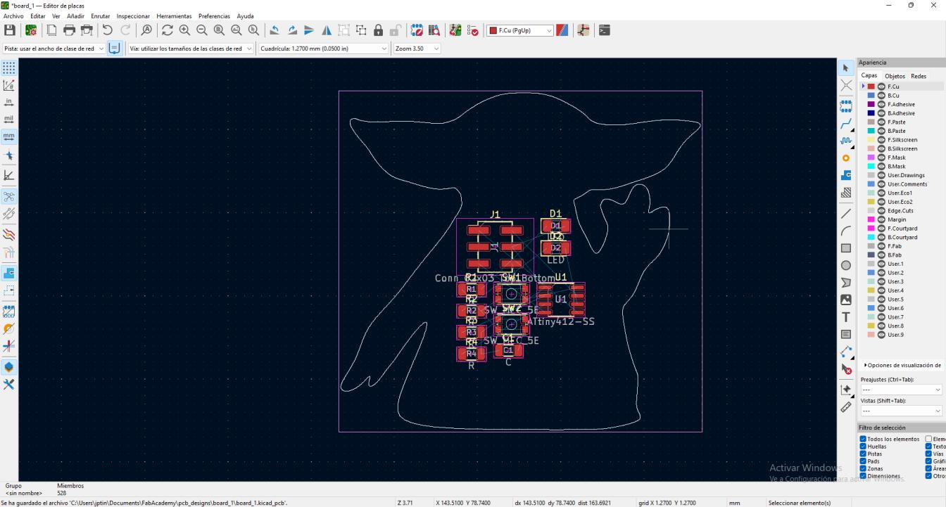
Figure N°28
We create a common ground in the Top layer.
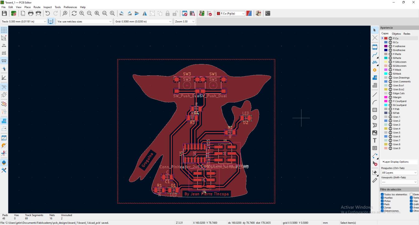
Figure N°29
One of the advantages of Kicad is that if we have the complete 3D model libraries we will be able to visualize a 3D model of what the PCB would be like.

Figure N°30
Another important tool is the Design Rules Checker, which informs us if there are problems within the design.

Figure N°31
Using it in our design gives us several warnings, such as references that are off the board and tracks that are connected to nothing.
Correcting all the requested parts, now we see that the DRC marks zero.

Figure N°32
With the complete design we can export the design in .VRML format and then import it from Kicad.

Figure N°33
We can see in Figure No.34 the model imported into Blender.

Figure N°34
We added colors to the textures to be able to recognize the parts.

Figure N°35
As with the outline of the PCBm we will make another design for Grogu's clothing.
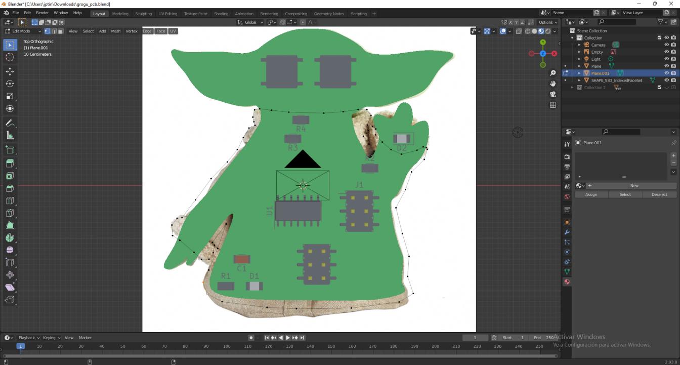
Figure N°36
We use subdivision surface to round the contour.

Figure N°37
We added details for the neck and wrists.
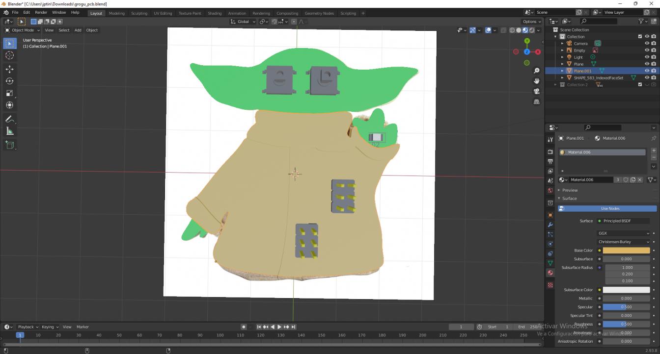
Figure N°38
We see the 3D model in Figure No.39
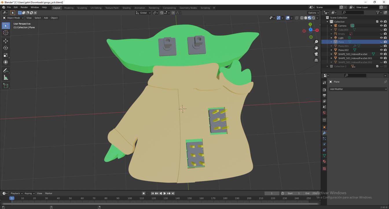
Figure N°39
In order for the clothing design to become a case, we must make another section that fits with it and encloses the plate. For this reason we added holes in 2 parts of the plate as shown in Figure No.40
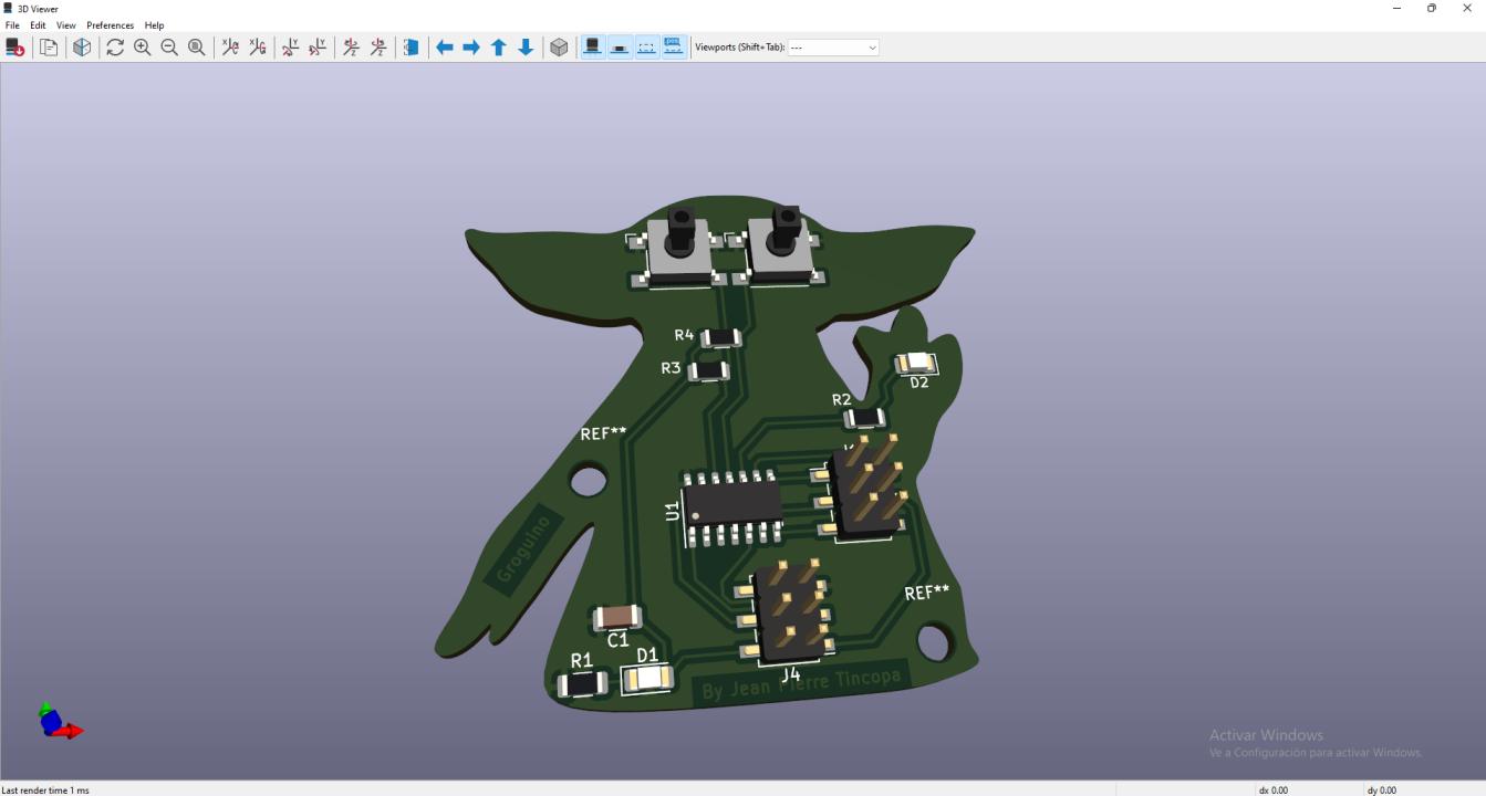
Figure N°40
Similarly in blender we make the lower part of the case and use a boolean difference to subtract the cylinders.
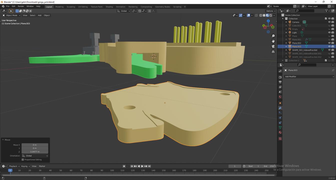
Figure N°41
The final design of the board with its case in Figure N°42
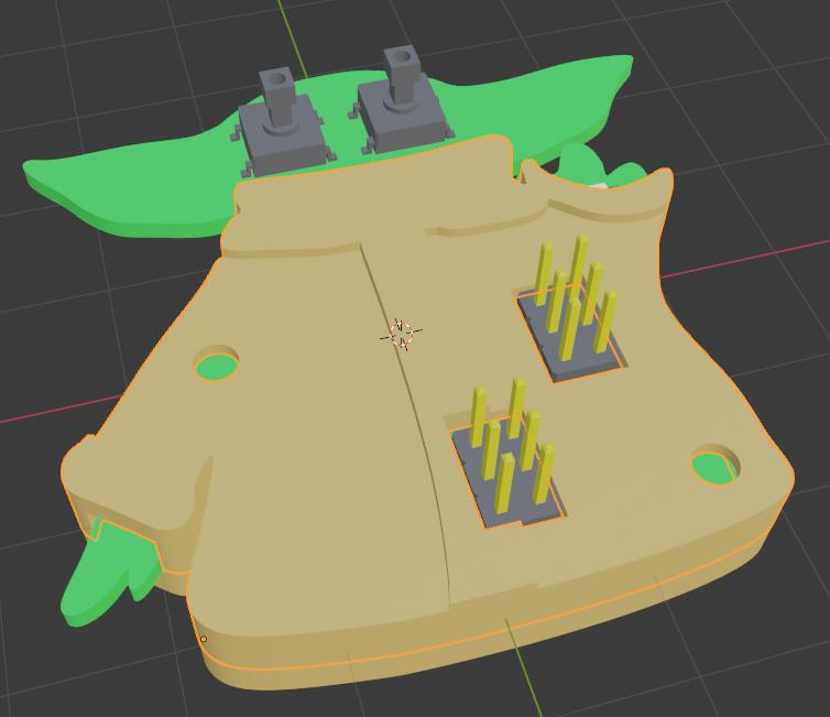
Figure N°42
The case was 3D printed with PLA filament.
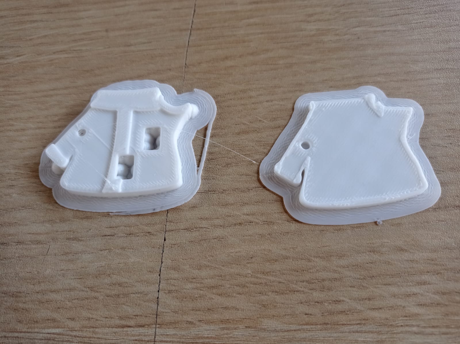
Figure N°43
With a couple of coats of acrylic paint, it is left with the right color.
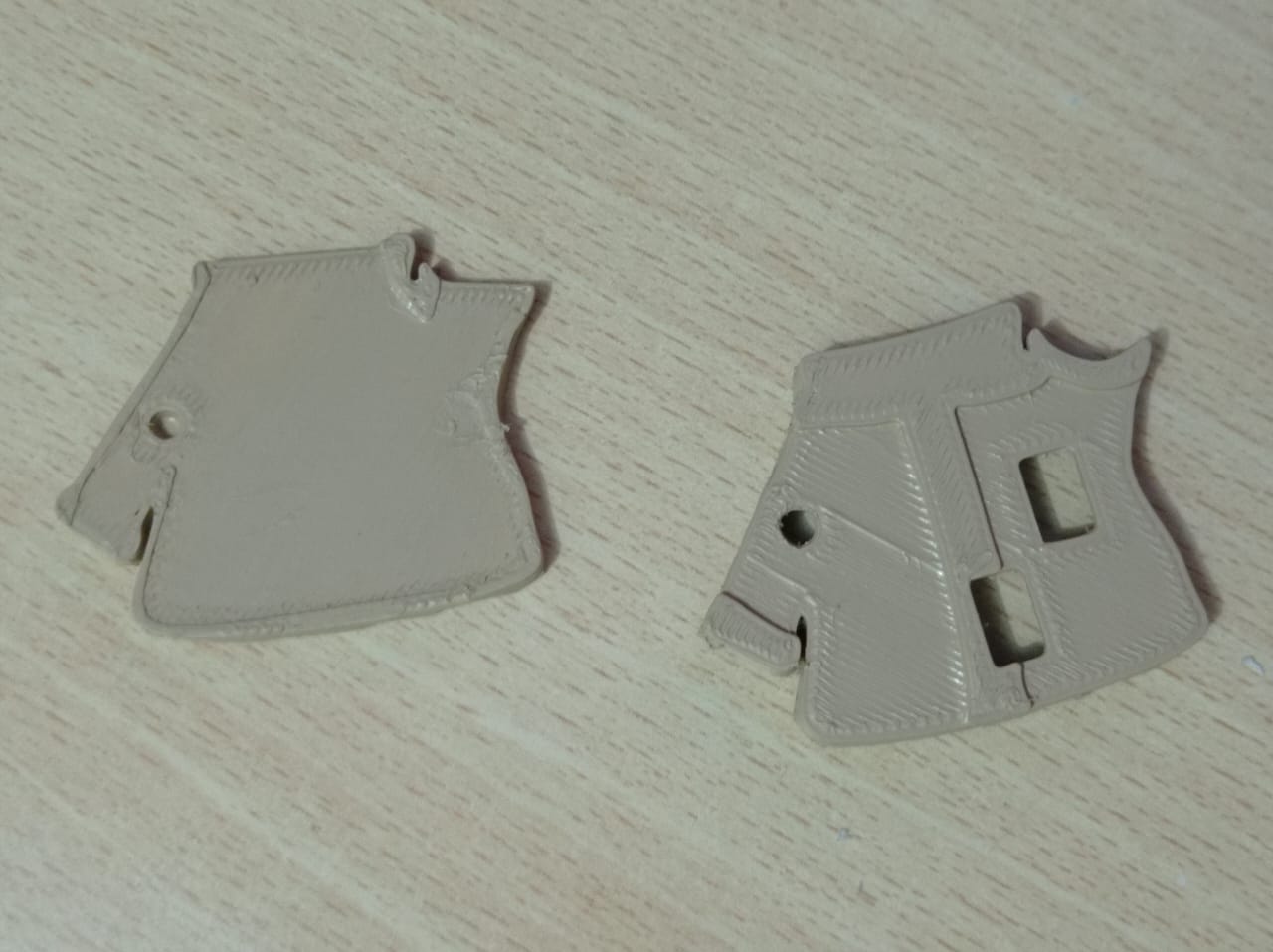
Figure N°44
The files created or used this week can be downloaded here:
| Kicad Files of Groguino | Link |
| Top of Grogu's Clothes | Link |
| Bottom of Grogu's Clothes | Link |