Fab Academy 2022
Hi,
My name is Fenil and this website will be the documentation of my journey through the Fab Academy course which consists of multiple assignments and a final project. A little introduction about me, I am from Gujarat, India. My area of interests includes eating and sleeping, been doing that of 22 years and still look forward to it every single day! I am doing the Fab Academy course from Vigyan Ashram. I was doing Bachelor of Commerce and completed my college in March 2020. For a long time I had interest in makingthingsI come across. I used to watch a lot of Do it yourself videos online and try to replicate them. I then found this guy called Shane who makes all kind of stuff, like he thinks of an idea and then proceeds to actually make it happen. I was highly motivated and wanted to achieve that kind of skills. However, I didn't have proper knowledge or resourse to execute any project on my own so it would take longer period of time than one would require(not to mention all the frustration). I talked to my sister about this and she recommended me to enroll for the Fab Academy course and so, here i am, experiencing the glimpse of digital fabrication in the hope that I will have a better, broader approach for my future projects.
Weekly assignments


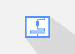


Drip Irritation
For my final project, i decided to continue the project i was working on earlier. The old project had a lot of things to improve and since i
decided to continue working on that project, it was
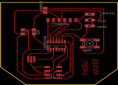
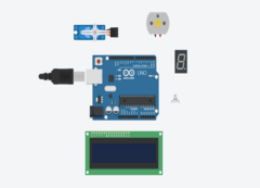
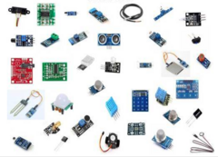
going to cover a lot of aspect of the fab academy like electronics production, electronics design, embedded programming, networking and
communication, interface and application programming, 3d printing, laser cutting and so on. I'll explain about the final project im detail
Problem Statement
In public places like bus station/railway station, i have observed a lot of times that due to wear and tear, the taps/faucets starts to leak
and due to the ignorance or the lack of communication, lots of water is already wasted before someone repair/replaces the tap,
Also a lot of times, people leave the taps fully or partially open after using it,
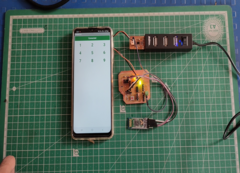
So i wanted to make a device that not only indicates when there is running water but also gives you the data about how much water is already
being wasted.
Read more...
Drip Irritation by Fenil Chandarana is licensed under Attribution-NonCommercial-NoDerivatives 4.0 International![]()
![]()
![]()
![]()