7. Electronics Desgin
# Goal:
Design an ATtiny44 echo board with a button and an LED, then program it
# Tasks:
1- Resketch an ATtiny44 echo board with a button and an LED using Eagle and FlatCam software. .
2- Fabricate an ATtiny44 echo board using a Roland SRM-20 CNC machine.
3- Soldering the circuit parts to the ATtiny44 echo board.
4- Program the ATtiny44 echo board.
# Procedures:
In week 5, I fabricated my first printed circuit board (PCB) using a CNC machine. PCB is the formal name for the board, which indicates the layout data, including the number of components. The purpose of PCB is to connect the electronic components by the conductive traces. For this week's task, we designed a circuit board before fabricating it. Engineer Hashim gave us a tutorial about sketching an ATtiny45 board using Eagle and FlatCam software.
a. Designing:
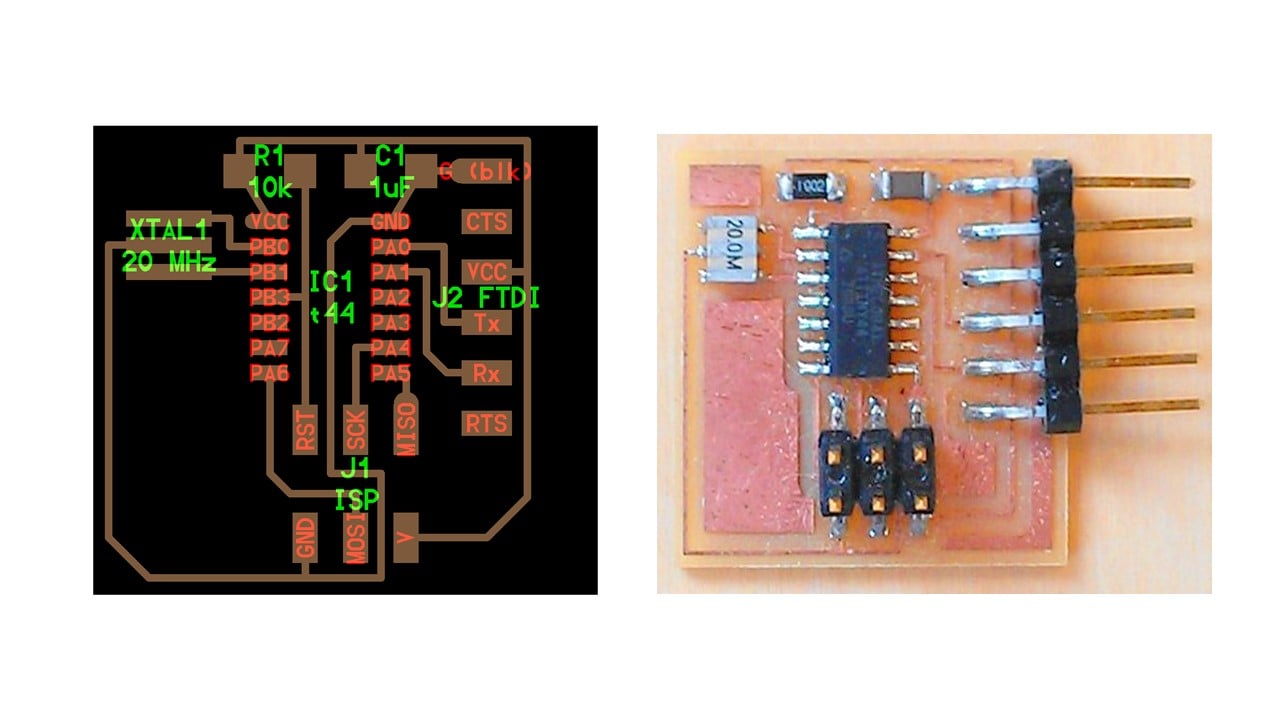
To start the designing process, I chose to fabricate the ATtiny44-echo board. I downloaded the board and components images for this echo board from this link.
Also, the engineer provided us with two Eagle software libraries specific to the FabLab. After downloading these libraries, I opened them in Eagle software and activated them by clicking on the gray dot to make it green.
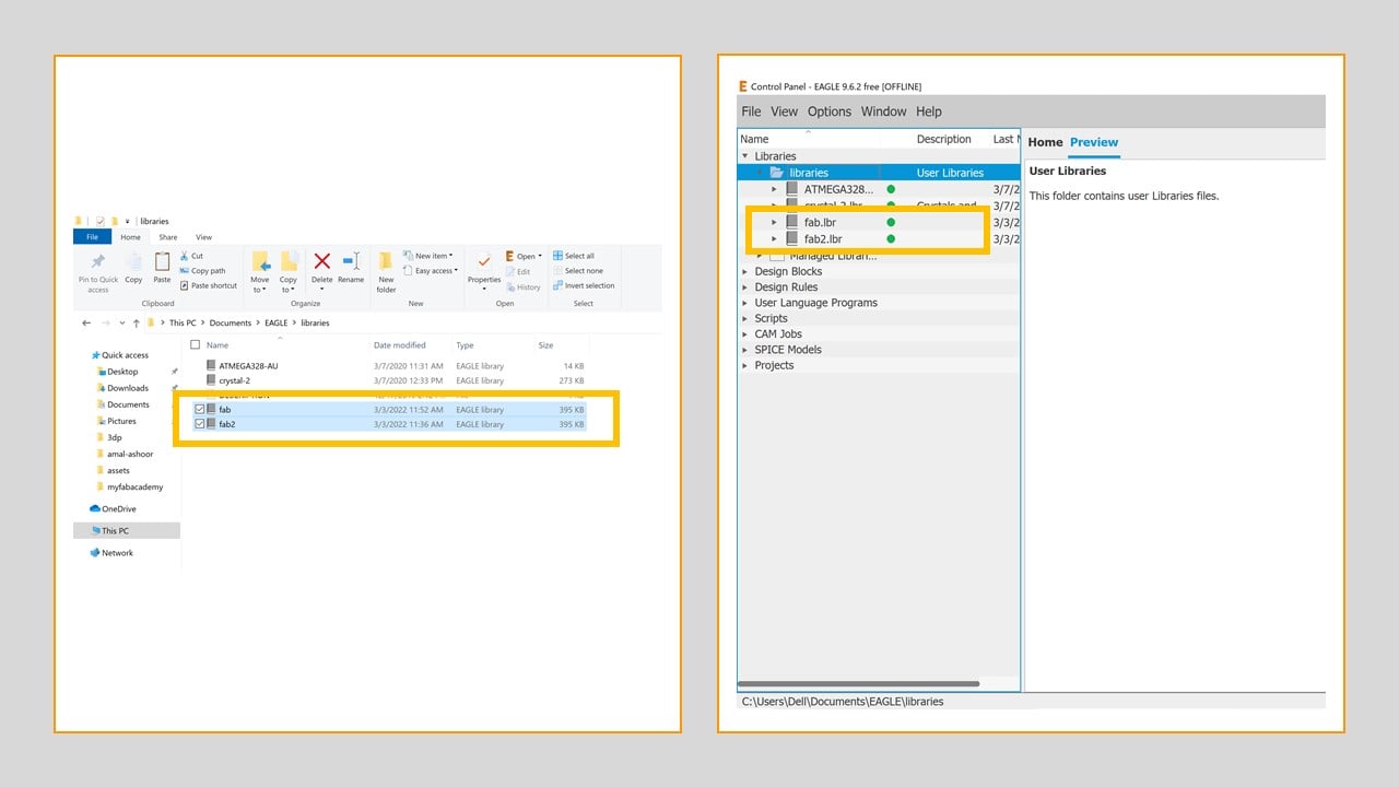
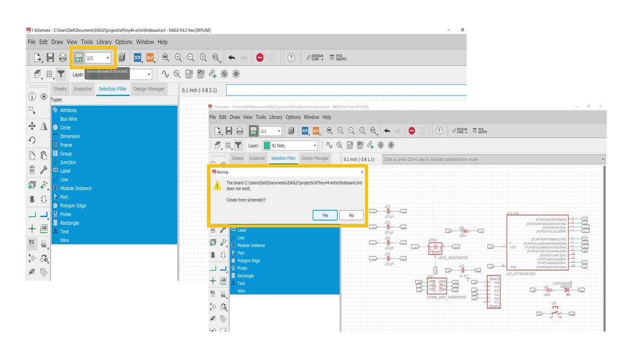
To create a new project on Eagle, I right-clicked on "Projects" and pressed on "New Project". Then, I named the project "ATtiny44-echo" and I right-clicked on "New" and pressed on "Schematic".

After the Schematic screen appeared, I enabled the grid feature and adjusted it to 0.1 inches. In the left toolbar, I used seven essential tools.
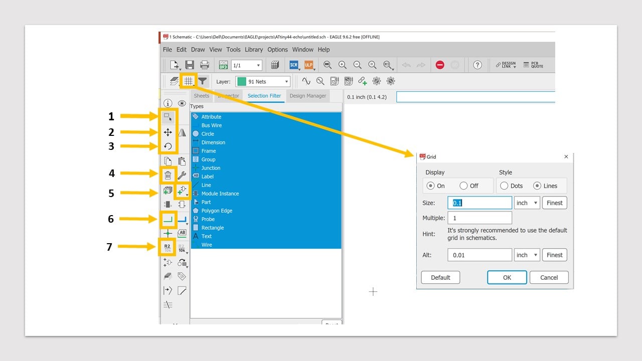
| Tool | Description |
|---|---|
| 1. Group | To enable different components to endure similar changes. |
| 2. Move | To move a component from one place to another. |
| 3. Rotate | To rotate a component by a specific degree. |
| 4. Delete | To delete a component or net. |
| 5. Add Part | To add a new electrical component. |
| 6. Net | To connect between the components. |
| 7. Name | To name the net and paths. |
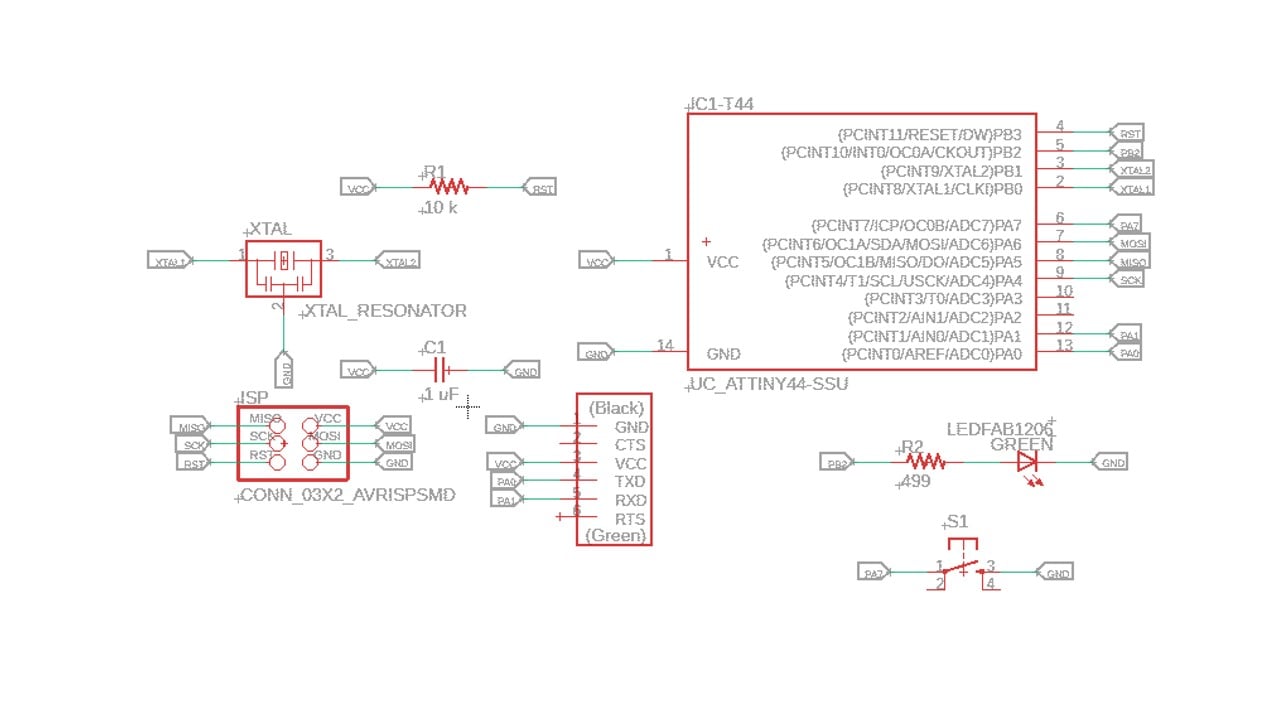
I used the "Add Part" tool to add the nine components of the board. These components are shown below. I started by adding the capacitor, then I right-clicked on its diagram to adjust the properties. For example, I fixed the value of the capacitor to 1 uF.

| Component | Quantity |
|---|---|
| ATtiny44 | 1 |
| 10kΩ Resistors | 1 |
| 499Ω Resistors | 1 |
| FTDI | 1 |
| Resonator | 1 |
| Button | 1 |
| Green LED | 1 |
| 1 uF Capacitor | 1 |
| 2x3 pin header | 1 |

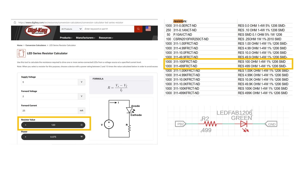
One of the requirements of the assignment is to add LED to the chosen board. So, I selected a Green LED. Then, I checked the Fablab inventory to learn more about the available Green LED. After I reviewed the datasheet of the LED, I learned that the maximum forward current is 25 mA and the LED typical voltage is 2 V.

Then, I calculated the current-limiting resistance that should be attached to the LED using this calculator. The calculator implemented ohm's law and Kirchhoff's law. The calculated resistance was 120 ohms, and this resistor is not available based on the Fab Lab inventory. To avoid operating a resistor at its maximum value, I chose a 499 ohms resistor as the limiting-current resistor.
I used the "Net" and "Name" tools to connect the electrical parts and name the paths, respectively. This is the resulting schematic diagram of the board.
I saved the file. Then, I pressed on the "Generate/Switch to board" to create the actual layout of the echo board.
In the board screen, I used the following six tools to draw the layout. Before I started, I moved all the components as a group to the inside the borders.
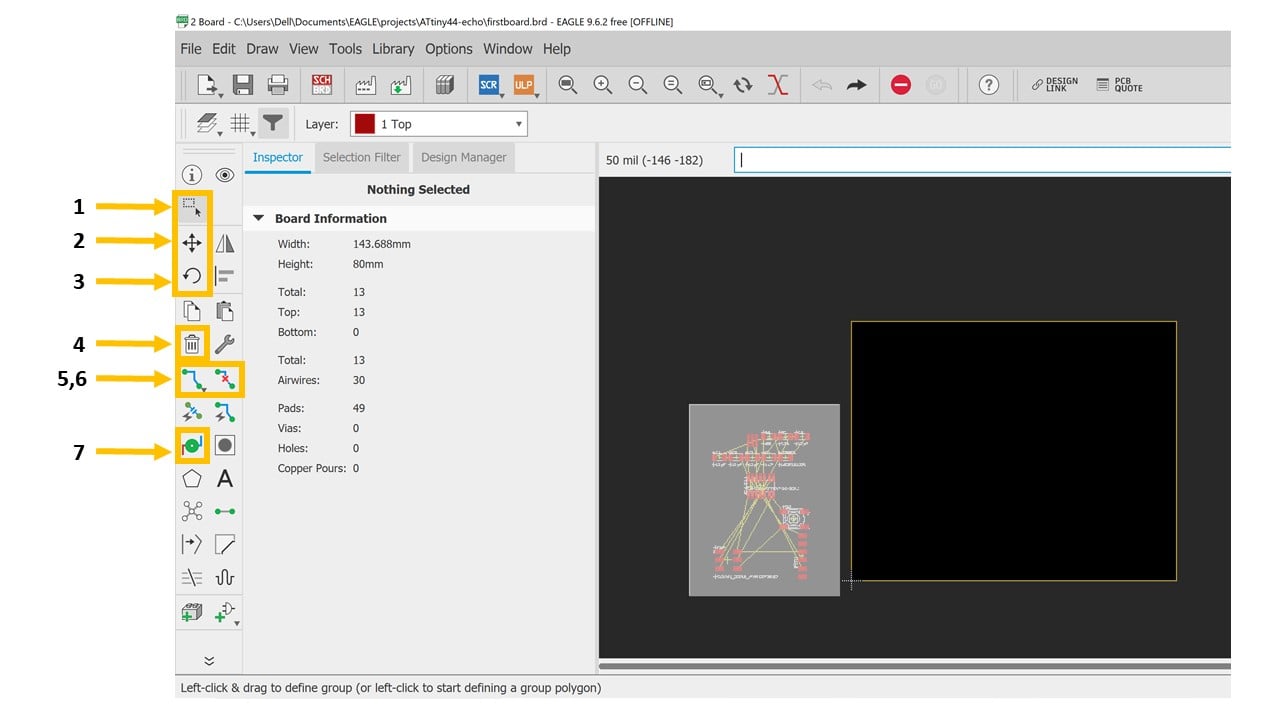
| Tool | Description |
|---|---|
| 1. Group | To enable different components to endure similar changes. |
| 2. Move | To move a component from one place to another. |
| 3. Rotate | To rotate a component by a specific degree. |
| 4. Delete | To delete a component or net. |
| 5. Route Airwire | To add airwires between the components. |
| 6. Ripup | To remove airwires between the components. |
| 7. Via | To add a hole. |
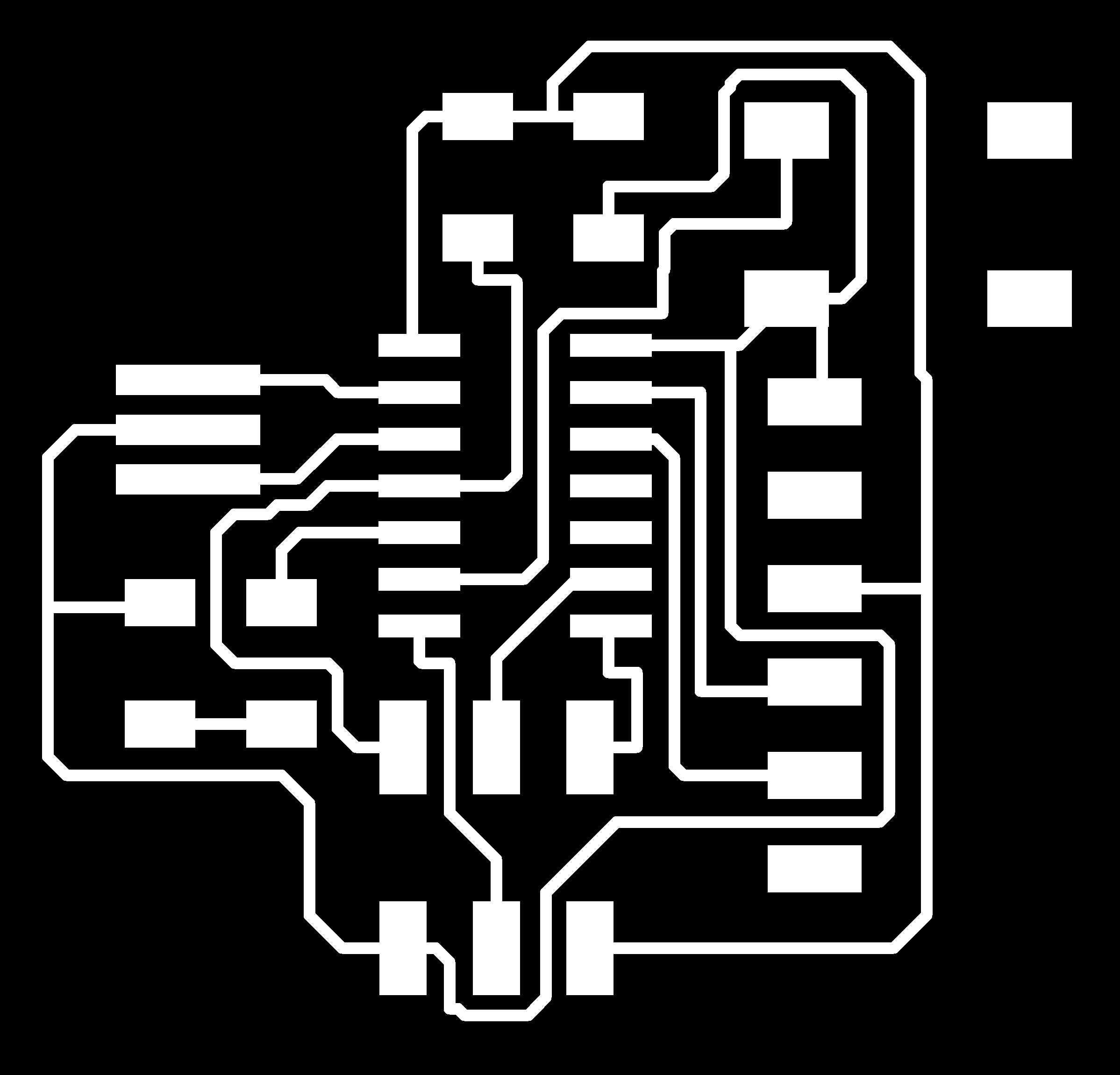
I connected the components as shown below after many trials. Then, I reduced the border's size to fit the exact size of the outline.
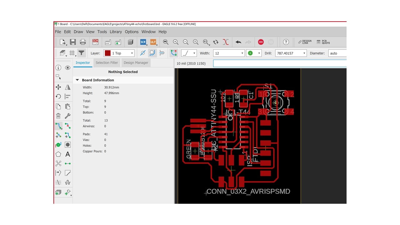
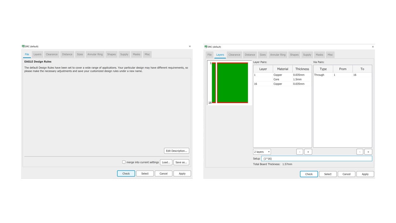
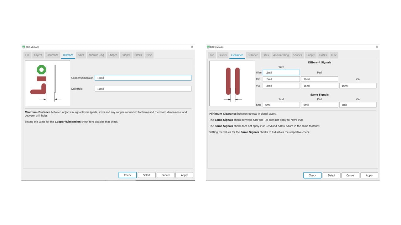
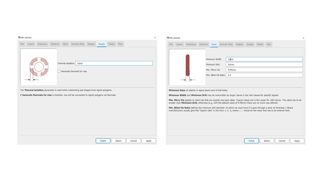
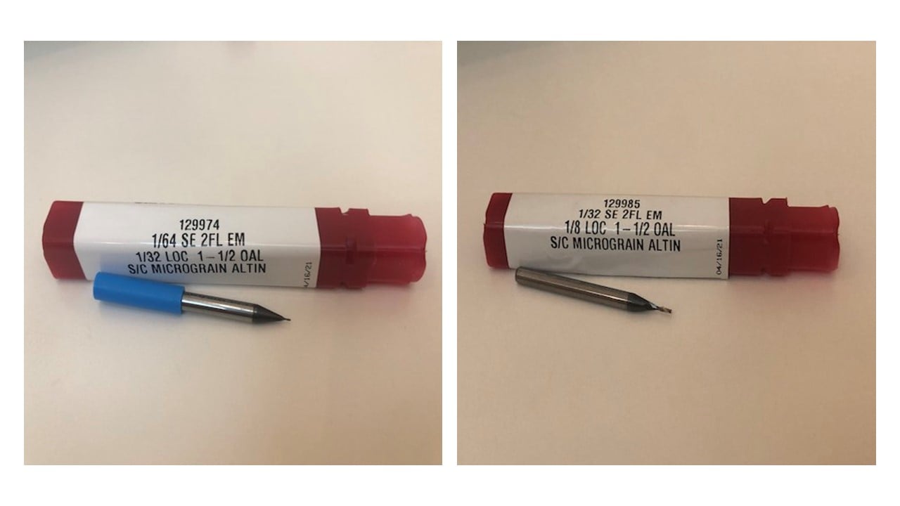
The final step is the design rule check. All the settings are shown below. Since I am using a 1/64 mm milling bit, which equals 15.63 mils, I round the clearance dimensions and distance to 16 mils.
After I received a "No Error" message, I saved the files.
b. Fabrication:
I transferred the Eagle files to CNC code files, which the Renold SMR-20 CNC machine can understand. To start this process, I used FlatCAM software to generates CNC code. For the outline, I opened the Garber file "copper_top". Then, I pressed on "selected" to adjust the settings. I started by changing the diameter tool to 0.4 mm, which equals 1/64 inches. After that, I increased the number of passes to 4 and their overlap to 60%. Also, I combined the four passes before generating an isolation geometry. Then, I fixed the Z-axis cut to be -0.1 same as the settings done in week 5. After that, I pressed on "Generate CNC Job Object" to generate the CNC code.

For the border, I opened the Garber file "profile". Then, I pressed on "selected" to adjust the settings. I started by changing the diameter tool to 0.1 mm, which equals 1/32 inches. After that, I kept the number of passes to 1 and their overlap to 10%. Also, I clicked on "Generating Isolation Geometry". Then, I saved the CNC code.
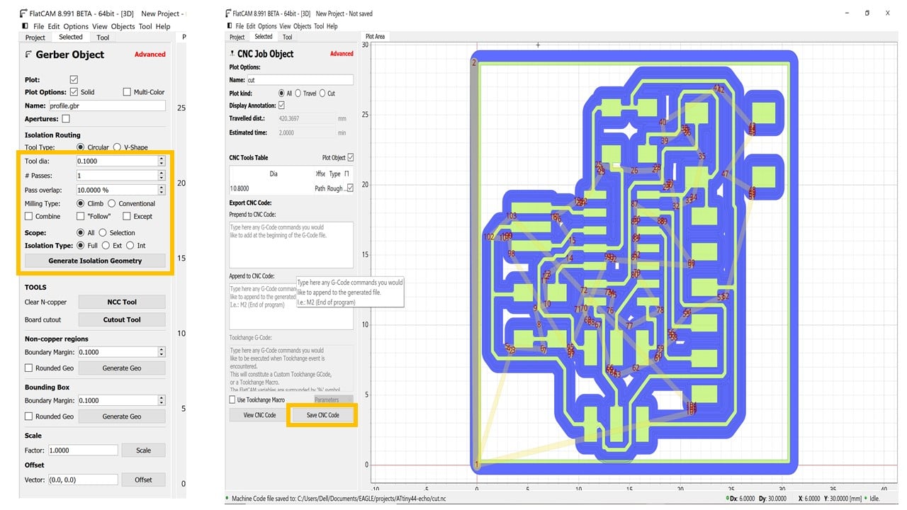
Moving to the Renold SMR-20 CNC machine. I started with placing an FR1-MDF board inside the machine and ensuring it was flat using the screws. Before milling, I changed the milling bit of the machine using a screwdriver to 1/64 milling bit for the outline and 1/32 for the frame. Then, I changed the machine to G54. I selected the origin point (X, Y, Z) based on the available space on the board. After that, I clicked on the cut button and added the CNC code files to start milling.
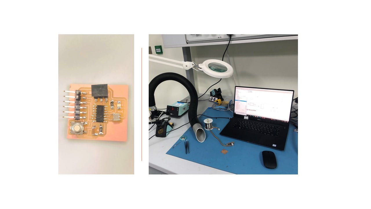
c. Soldering:
First of all, I collected the 9 components of the circuit. I used double-sided tape to stick the components on paper to avoid losing them since they are tiny. I started the soldering process by adding solder to PCB pads with one hand and try to move the circuit components by the other. I Kept repeating this process for all the components. To avoid having a short circuit, I removed the excess solder and I checked the ends of the components using a multimeter.
d. Programming:
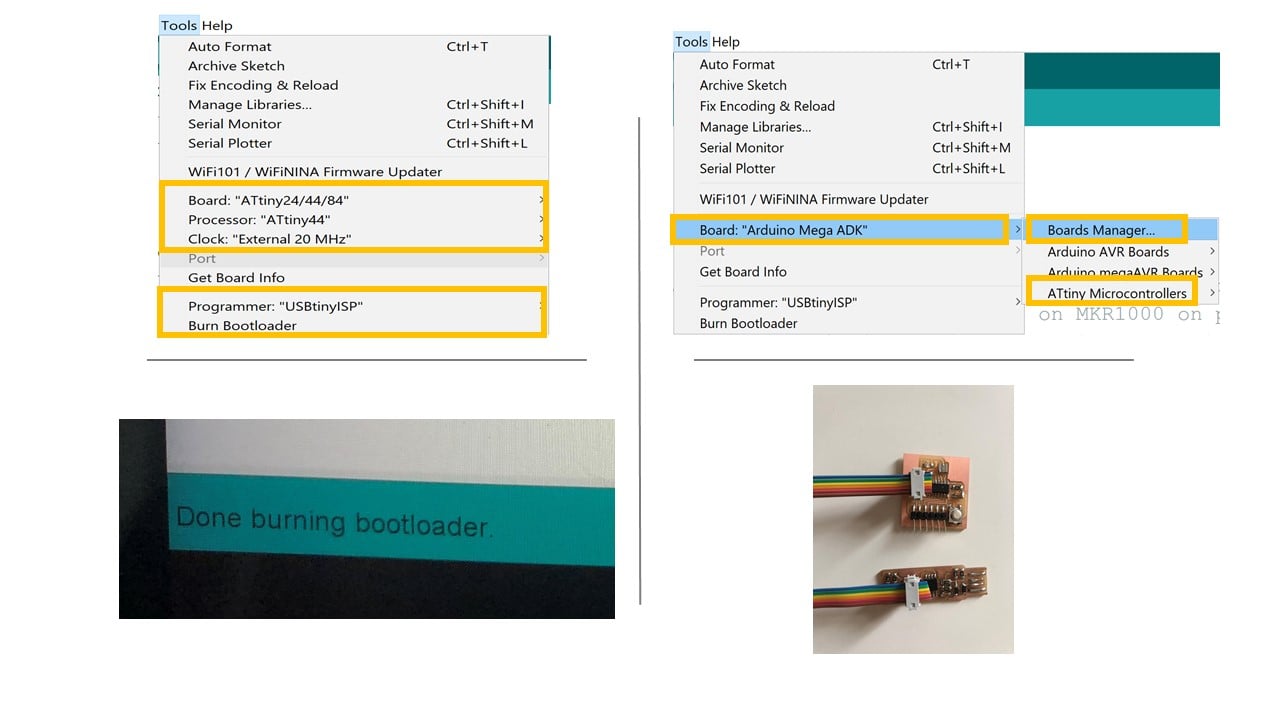
Before programming the ATtiny 44 echo board, I fixed two 2x3 connectors at the ends of a ribbon cable using a hammer. Please notice that the order of the colors on both ends must be the same. To program my board, I connected it to a previously programed FabTinyISP by the ribbon cable. Then, I downloaded Arduino IDE from this website and connected it to the ISP using the ribbon connecter as shown below. Then, I clicked on Tools and change "Board", "Processor", and "Clock" as shown below. After that, I selected the programmer by clicking on Sketch then "Burn Bootloader".
Group Assignment
The link of the group assignment page is here.
# Goal:
Use the test equipment in your lab to observe the operation of a microcontroller circuit board.
# Task:
Use the multimeter to show the change in the voltage in the ATtiny44 board.
# Procedures:
I used to measure the voltage of the board using the multimeter, by connecting the black and red ends to the board GND and the VCC, repectively. As you can see, the voltage is around 5V when the button is pressed.
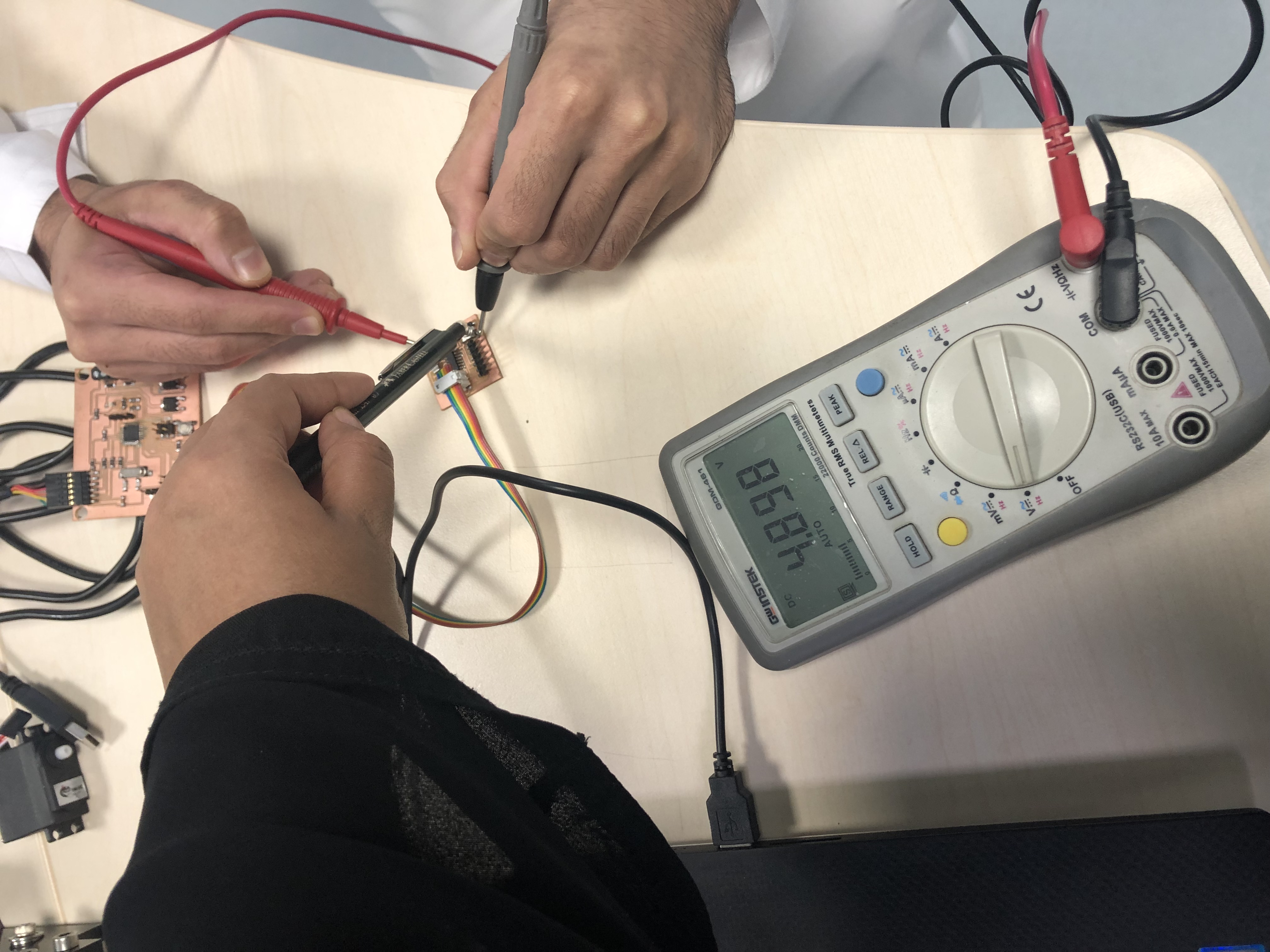
However, it become 0V when the button is released.

# Challenges:
I did face two main challenges. The first was during soldering, where the copper traces ribbed off the board, so I fabricated another PCB. The second challenge was during the programming process, my laptop could not identify my FabTinyISP, so I changed the used laptop.
# Files:
1- ATtiny44 Brd
2- ATtiny44 Sch
3- Traces PNG
4- Outline PNG