Week6- Electronics design
Introduction
Currently I am attending both fab-academy and fabzero. Since Bhutan is under lockdown, I had to work in containment zone along with Fran, Sibu and the SFL team in superFablab to set up the lab. So luckily for me, I had access to all the machines (Lots and lots of machines) but sadly we dont have Roland SRM20 with us but we have jake's clank machine.
Assignment
group project:
- use the test equipment in your lab to observe the operation of a microcontroller circuit board
individual project:
- redraw an echo hello-world board, add (at least) a button and LED (with current-limiting resistor)
- check the design rules, make it, and test that it can communicate
- extra credit: simulate its operation
Group assignment
The group assignment is here
Milling machine
The machine: Jake's clank machine
Softwares: KiCAD, mods CE, inkscape, Clank controller
Designing a PCB board
I used Eagle during the pre-fabacademy and started using kiCAD during the fab-zero program. After using both the softwares, i personally prefer kiCAD. So for this week, i used kiCAD to design my hello-world board. KiCAD is an open source software and i personally found it easier to design board in kiCAD than in eagle.
Tutorial on kicad= kiCADtutorial
Here are some of the keyboard shortcuts in KiCad
Editing a schematic
-
a- To add components. -
c- Copy a component when the cursor is over another component. -
w- To wire components. -
v- Edit component value. -
Esc- Escape mode or whatever command in progress and return to normal pointer mode. -
ctrl+z- Undo. Use liberally to undo any mistakes. -
ctrl+s- To save. Make sure to save often!
Editing a PCB layout
- Press to switch to the next layer= + -
- Press to switch to the previous layer= - -
- Move item= m
- Update ground polygon pours= b
- Remove a trace or component= Delete
- Route new track= x
- Add through via= v
- Next grid size. Use with caution. There will be tears if you use a grid outside of 50mils or 25 mils= n
- Return to the top copper layer= Page Up
- Escape mode or whatever command in progress and return to normal pointer mode= Esc Undo.
- Use liberally to undo any mistakes= ctrl+z
- To save. Make sure to save often!= ctrl+s
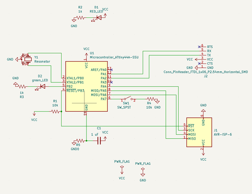
Hello-world board
Steps for creating a schematic file
-
Click on file-> new project or click new project on the top menu and name the file
-
Open the schematic
-
Add the components
-
Connect the components using add a wire
-
Right click on the components and click properties and assign values
-
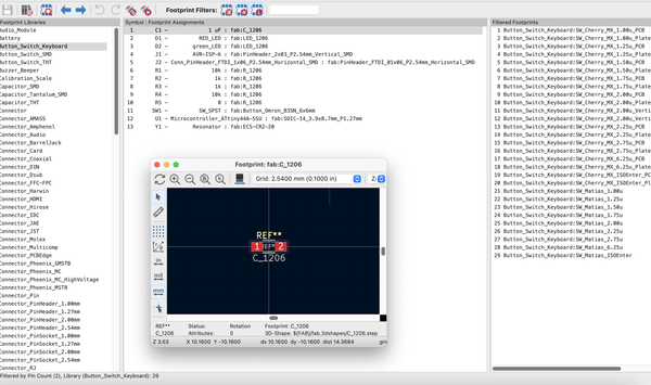
Click on tools ->assign footprints and select footprints for each components
-
Click on inspect-electrical rules checker to check if there are any errors
Steps for creating a PCB layout
-
Click on PCB in board editor on the top menu and a blank page opens up
-
Click on update PCB with changes made to schematic and update the PCB
-
Arrange the components #Grid-5mm
-
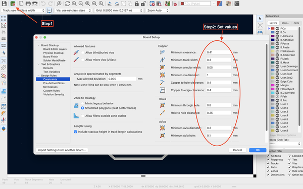
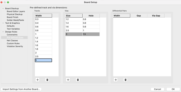
Click on edit board setup-> design rules->constraints and set the parameters
-
Click on predefined sizes under design rules and set the parameters
-
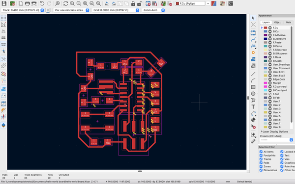
Click on route tracks on right side of menu and route the track connections (Click on route->interactive route setting and select shove option)
-
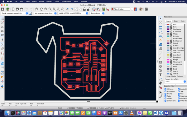
Click on draw a line on the right menu and draw the edge.
-
Right click on the edge line and select properties and choose the line width 0.8mm(for fablab machine)
-
Click on view- 3D viewer to see the board in 3D version
-
Route the tracks. Press W while routing the tracks to change the width
-
Click on inspect->design rules checker to see if there are any errors
To save the file
Click on file->plot
- To save gerber file
-
Plot format= gerber
-
In include layer, choose both F.Cu and edge cuts
-
In general options
Choose plot edge .cuts on all layers Choose check zone fills before plotting -
Click on plot
- To save svg file
-
Plot format= svg
-
In include layer, choose F.Cu
-
In general options,
Choose plot edge .cuts on all layers Choose check zone fills before plotting Choose negative plot -
Click on plot
-
Plot format= svg
-
In include layer, choose edge cuts
-
In general options,
Choose plot edge .cuts on all layers Choose check zone fills before plotting -
Click on plot
- Inorder to have a file in png (mods accept png files), open the svg file in inkscape
- Open the svg file in inkscape
- Shift and select the image
- Click on file- document properties
- Click on resize page to content- resize page to drawing or selection
- Click on file- export png image
- In dpi, give 1500 resolution
- Click on export (make sure to select the folder in which u want to save the png image)
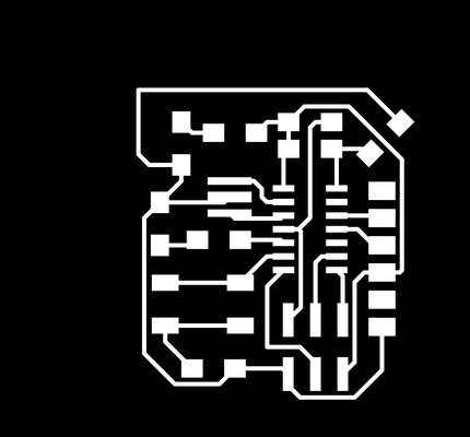
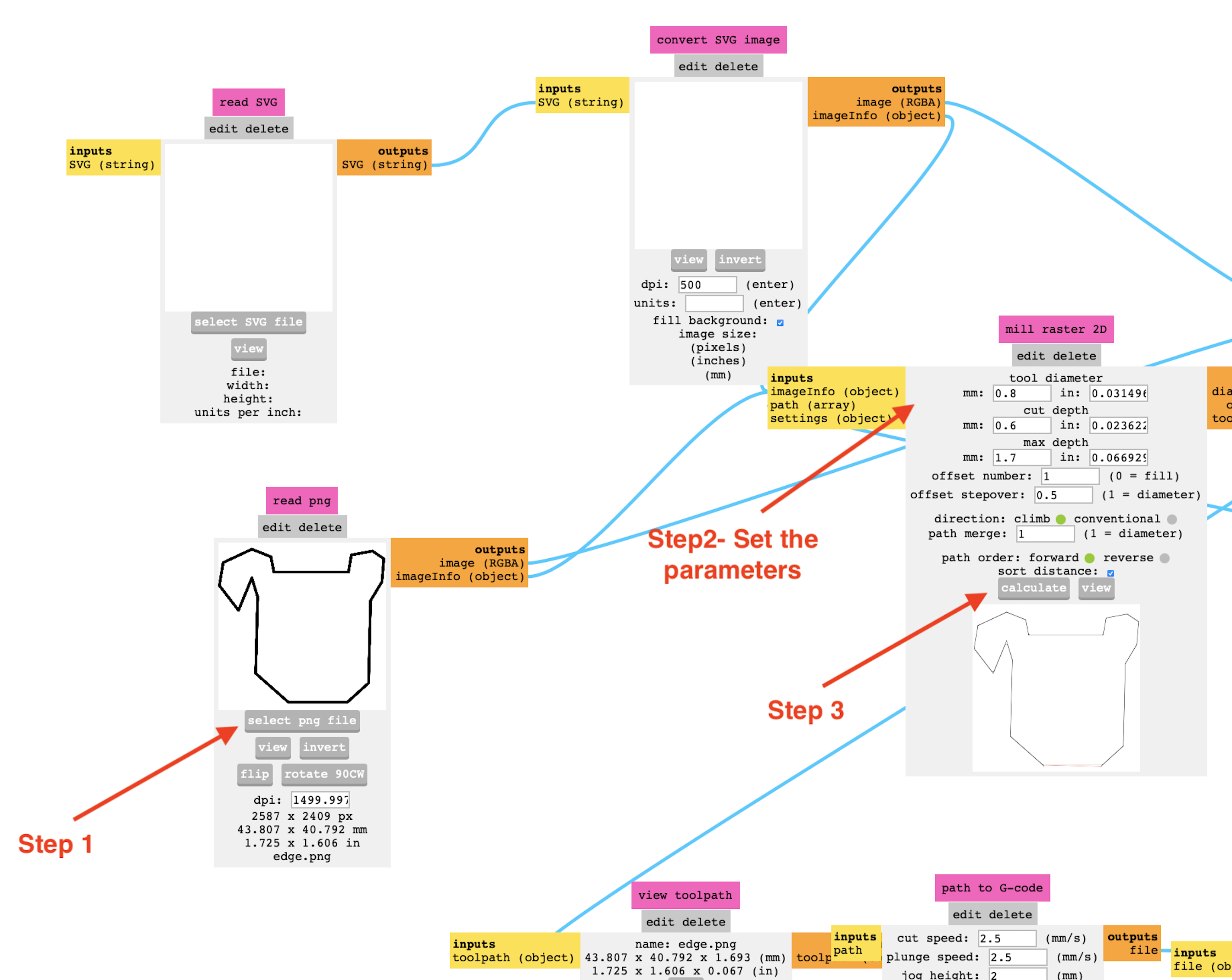
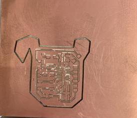
The traces of the board
The edge of the board

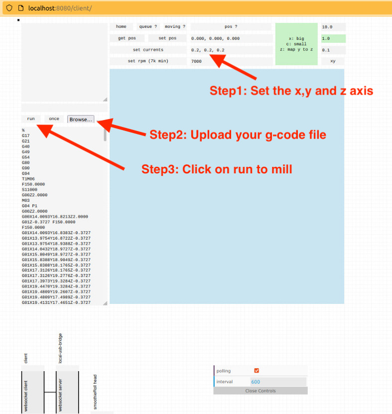
Mods
-
Go to mods
-
Right click-> programs-> open grograms-> g-code-> mill 2D PCB
-
Open the png image and then calculate to get the g-code file for traces
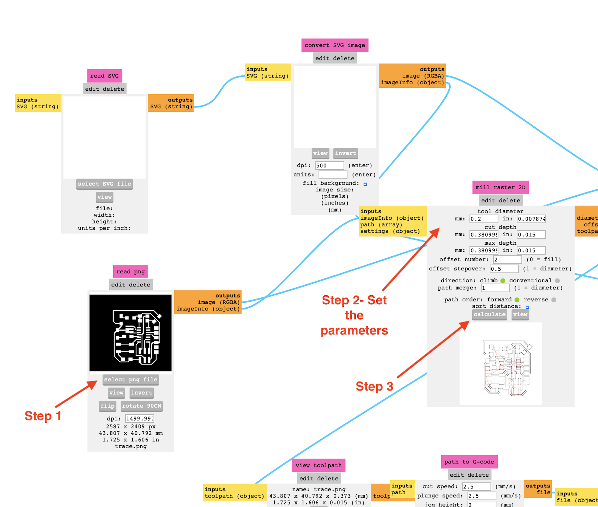
-
Open the png image and then calculate to get the g-code file for edge
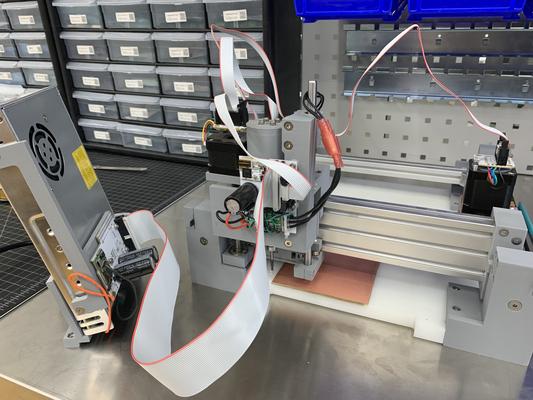
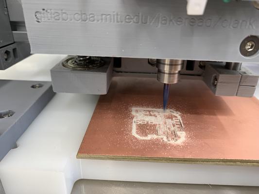
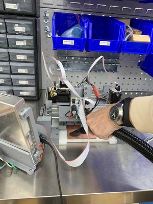
Jake's clank LLZ machine
I had to use Jake's clank LLZ machine in place of Roland SRM20 because some of the machines have still not reached the super fablab and Roland machine is among one of them. But it was fun to use a different machine. Although the Jake's machine was vibrating alot while milling and since it doesnot have a lid and i had to keep vaccuuming in between. It is not very user friendly, but at the end of the day, my weekly assignment is done thanks to the Clank LLZ machine.
- End mill
-
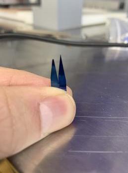
Since jake's clank LLZ machine was not very stable, I had to use V-bit end-mill instead of 1/64" end-mill for the milling the traces and 1/32" end mill for the edges.
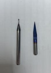
-
Make sure to use only the sharp V-bit 15 degree 0.1mm end mill for milling the traces of the board.
-
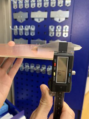
Copper board
Milling the board
After getting g-code file from the mods, i started milling the board
I used V-bit to mill the traces
I used 1/32 end-mill to mill the traces
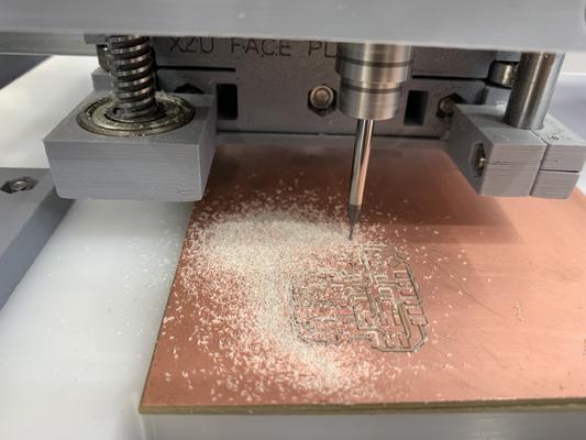
#Note: While milling, ensure to keep a vacuum cleaner near the jake's clank machine since alot of dust is produced and the machine doesnot have an enclosing lid. So, vacuum while the machine is in operation.
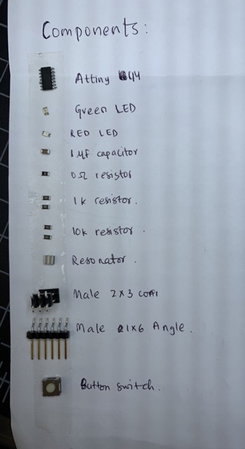
Soldering
-
List the materials and assemble them. Solder the components one by one (Tip- Start with soldering the microcontroller first)
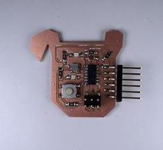
Programming the Hello-world board
-
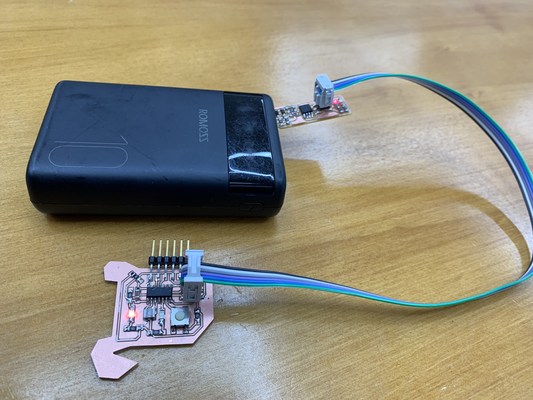
First test to see if your hello-world board is working properly and do not have any short circuits. For that, try to connect to a power bank rather than connecting to the usb port of your laptop as it can damage the usb port of your laptop. The red LED indicates the power supply is present.
-
To prgram the hello-world board, i am using arduino software. To add the attiny to the arduino, follow the instructions here.
-
I programed the blink program to the hello-world board but the green LED wouldnot blink.
Trouble shooting:
-
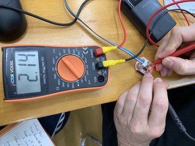
When i measured the voltage between the VCC and the GND of the ATTINY 44 microcontroller, i found that the volatge was 2.2V instead of 5V.
-
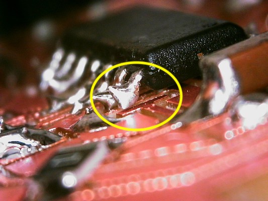
I looked under the microscope and found that the ground of the ATTINY 44 microcontroller was just floating in the air. I rectified it.
-
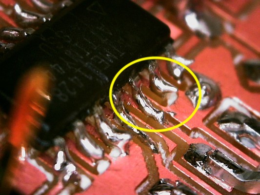
But it still wasnot working, so I performed continuity test using multimeter and found that the PB2 pin and PA7 pin was cold soldered. I kept the soldering iron on the PB2 pin and PA7 pin so let the soldering iron melts downwards.
-
-
As I connected the hello-world board to the supply, the Green LED started blinking.
😊
The design files
The files of the following list is here
- The schematic of hello-world board
- The PCB file of hello-world board
- Gerber file of hello-world board
- SVG file of hello-world board
- PNG images of traces and edge
- G-code file of hello-wrold board