ELECTRONICS DESIGN
This week I designed, fabricated, and programmed a printed circuit board.
In Week 5, I learned how to mill and solder components onto a printed circuit board. This week I built on that knowledge to create and program a PCB that I designed myself.
Here was the assignment:
- Use the test equipment in your lab to observe the operation of a microcontroller circuit board (check operating voltage on the board with multimeter or voltmeter and use oscilloscope to check noise of operating voltage and interpret a data signal) (in groups).
- Redraw one of the echo hello-world boards or something equivalent, add (at least) a button and LED (with current-limiting resistor) or equivalent input and output, check the design rules, make it, test it.
Group Work
In the group lab, Professor Goodman showed us how to use a multimeter and oscilloscope. These tools can be very helpful in debugging a circuit board by checking the voltage in certain places. We tested our equipment on a circuit like this.
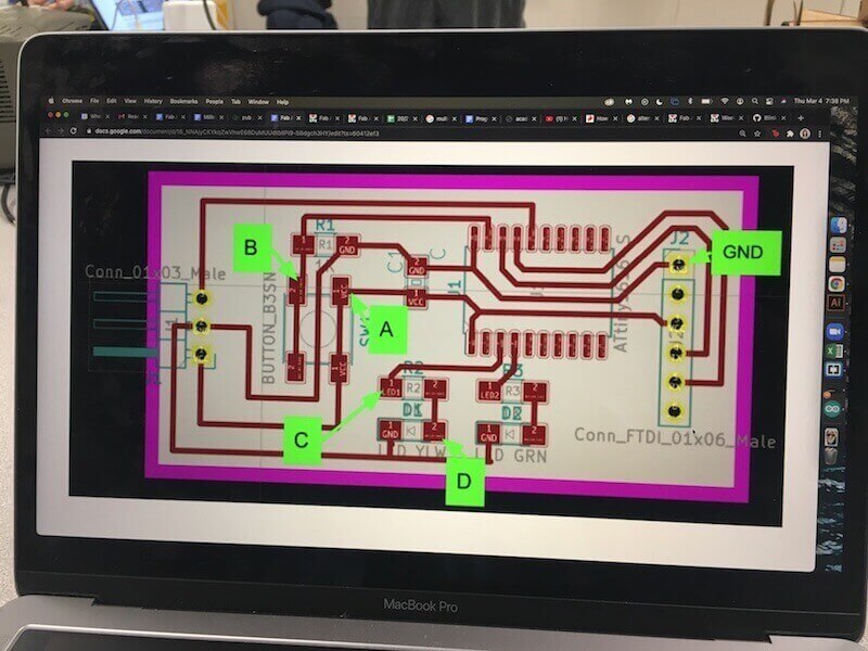
We used the multimeter first, setting it to the DC voltage mode. On the multimeter the black lead goes to GND. These were our readings when we placed the red lead at various points:
- A = 5 v
- B = .5 mv
- B (and press button) = .5 mv changes to 5 v
- C = 5 v
- D = 1.68 v
Notice that 5v is the voltage value from the power supply. Also, before we pressed the button, at point B, there was basically no change in current since the circuit was open and charge wasn't flowing. Between points C and D, the voltage dropped after going through a resistor.
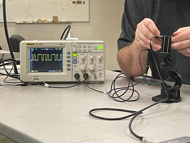
Next, we used the oscilloscope to observe the circuit's voltage noise. On the screen, the oscilloscope showed a graph of the voltage over time. This device can measure electrical signals at a much higher frequency than a multimeter, and we were able to zoom in to see the data signal in terms of individual voltage bands (1 for 5 volts, 0 for GND).
Hello World Board
Circuit Design
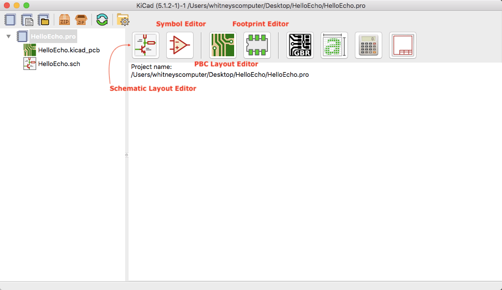
During the Thursday lab, Professor Goodman gave an introduction to KiCad, an electronics design software. I downloaded this program, along with the FabAcademy's KiCad libraries (this is a collection of symbols and footprints of the components that we're likely to use in class). I added those libraries to the program's existing ones via Preferences > Manage Symbols/Footprint Libraries.
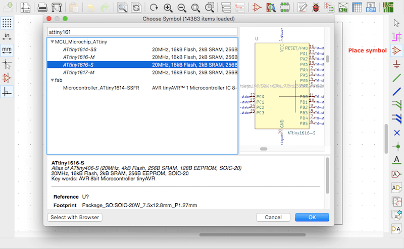
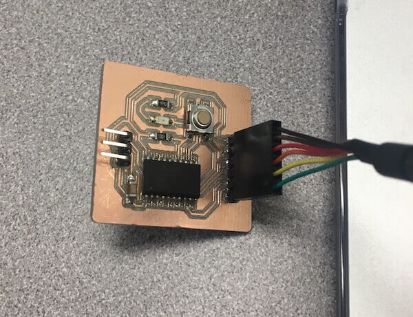
My job was to redraw the echo hello-world board, but with an LED and button. Given the components we had available in the Lab, I made my board with an ATtiny1616 and through-hole header pins. Professor Goodman provided our class with a circuit drawing of the hello-world board to start with.
Designing in KiCad works in two main steps,
- A schematic set up where you indicate what components are connected
- A footprint layout which shows the actual shape of components and where their traces will be routed.
To begin, I added components to the Schematic Layout Editor, referencing Prof. Goodman's drawing and some datasheets to make sure that they were the right components I needed.
I joined these components together, with the wire tool, again referring to the example circuit.
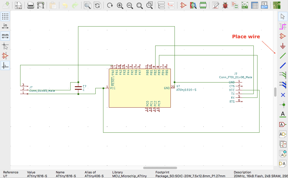
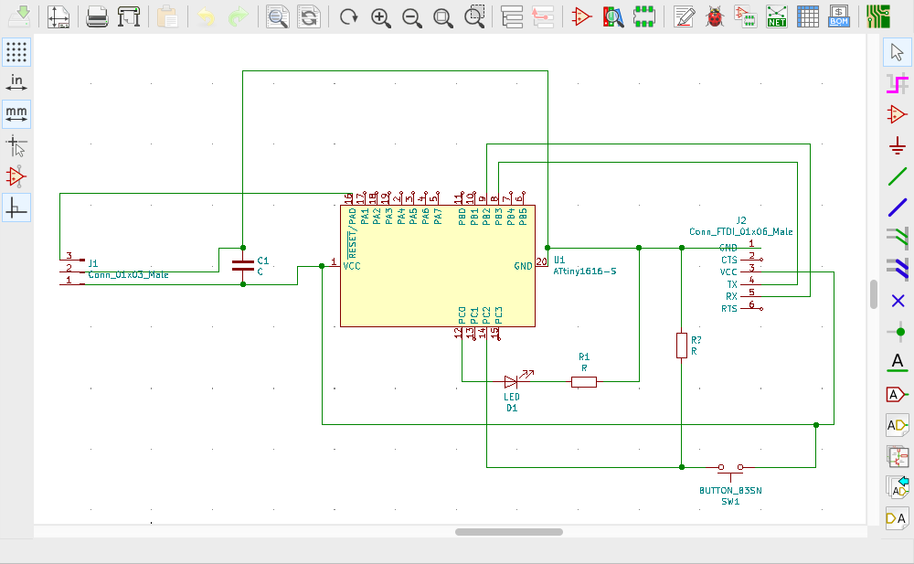
Next, I needed to place the LED and button. After a few attempts and some advice for Prof. Goodman, I was able to get the wiring correct. I also checked out these Arduino and Tinkercad sites to help me understand electrical needs of the new components. The LED receives power from a digital pin and requires a current-limiting resistor before the charge reaches GND. The button, powered by the VCC on the 1x06 pin header, sends a signal to a different pin, and uses a pull-down resistor before connecting to GND.
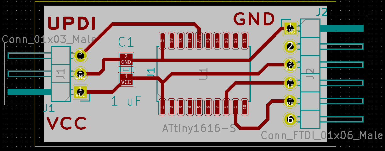
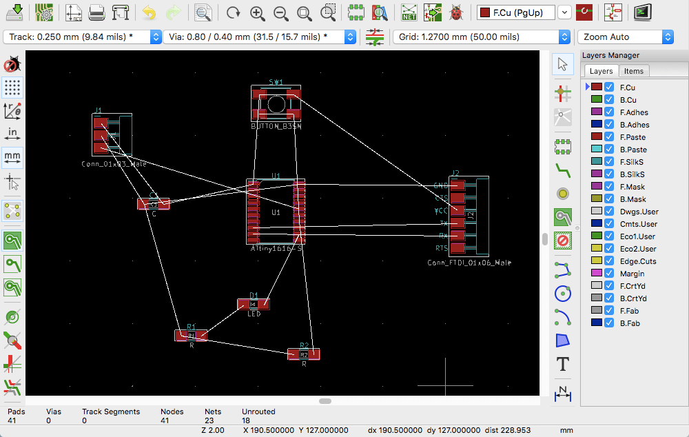
Once I had a schematic diagram, I opened up the PCB Layout Editor. Here I clicked "Update PCB from schematic". This imported my components and wires which I could then edit.
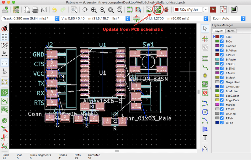
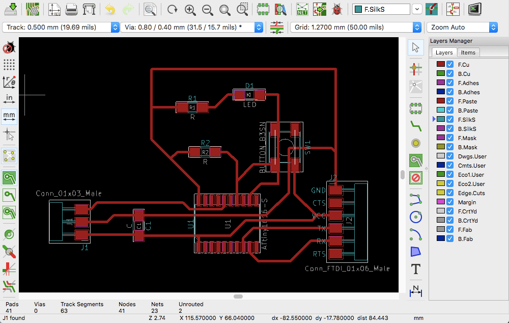
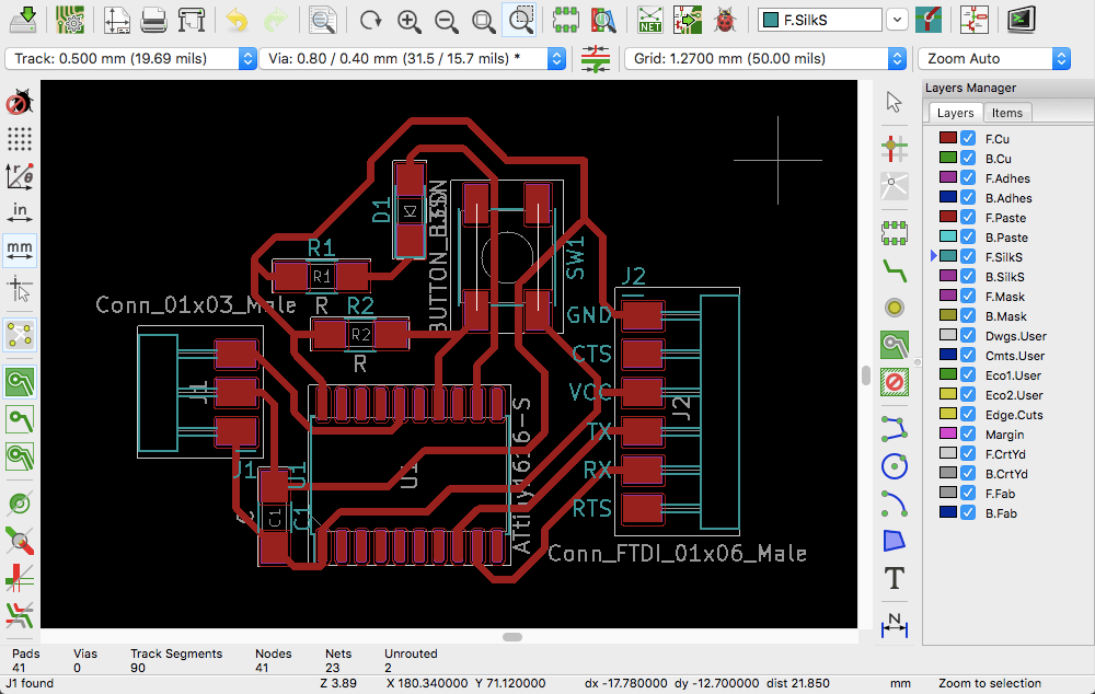
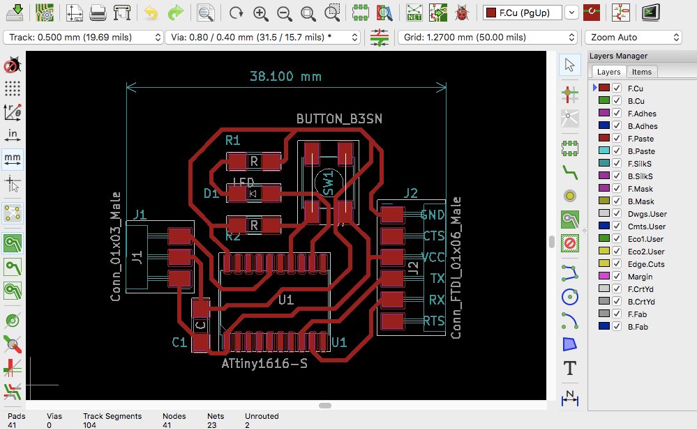
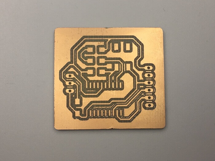
The PCB Layout Editor was where I arranged the footprints and traces to be machined by the mill. Footprints are the copper shapes on a PCB where components are mounted. These, in combination with the traces, give the components their electrical connection. When routing the traces, my main objective was to make the board electrically sound, meaning no overlapping wires that could cause a short circuit. To do this, I moved around the components and replaced the white schematic lines for red tracks.
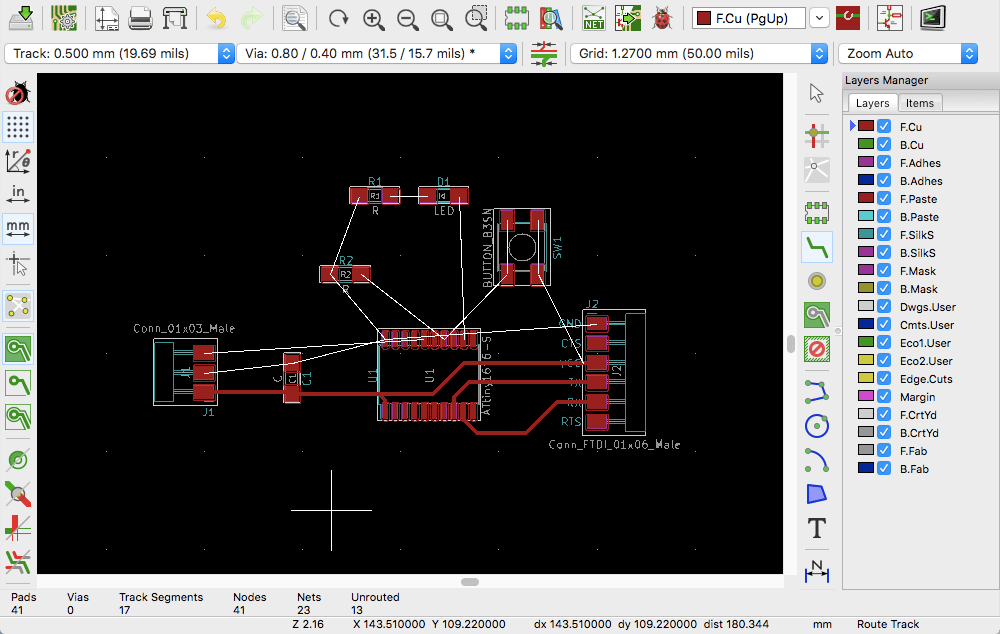
This was an interesting, new kind of challenge. The white lines kept shifting when I repositioned the components, and the paths were hard to decipher in that state. I found the best way for me to go about routing was to do the simple, one-to-one connections first, like the pins for transmitting and receiving data (TX & RX). Then, I created the main tracks for VCC and GRN. After that, I connected the peripheral components in any way I could.
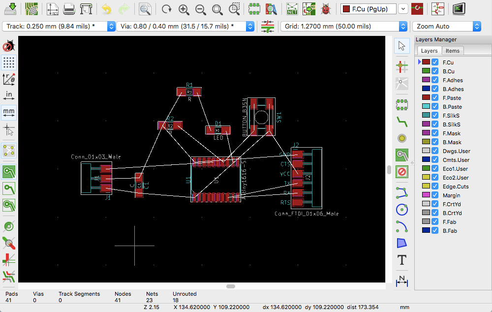
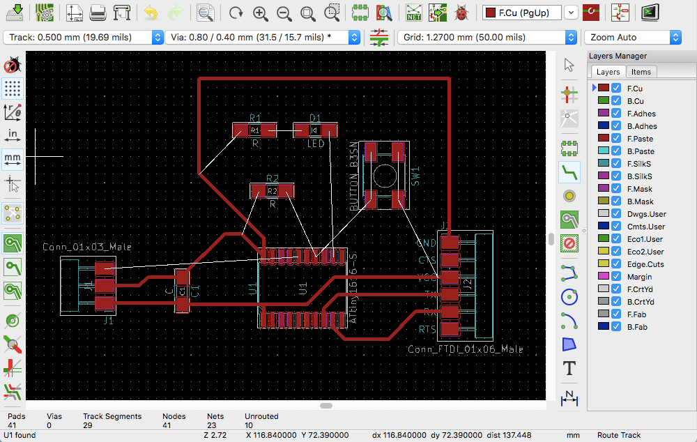
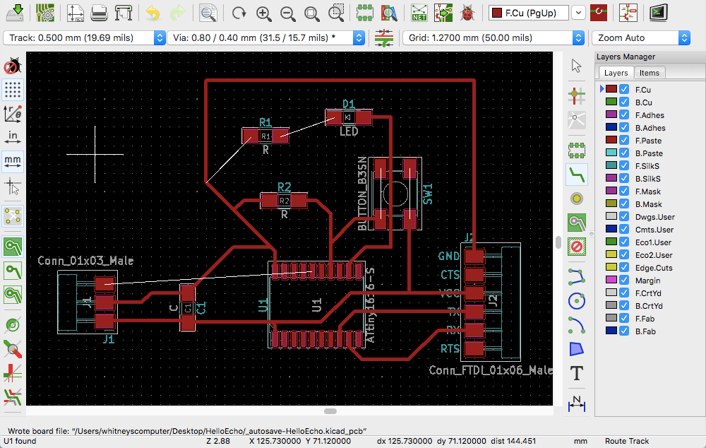
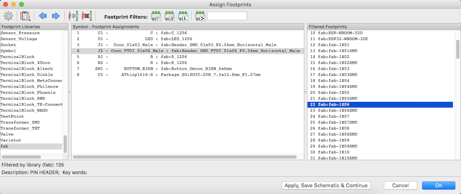
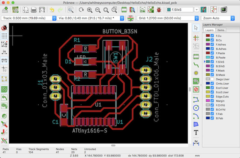
At some point I had to switch out the footprints for the pin headers because I was using through-hole instead of surface mount pins. I followed these instructions from Prof. Goodman, to go back to the Schematics Layout Editor and change the assigned footprints for the components. Notice how afterward I have holes for both pin headers.
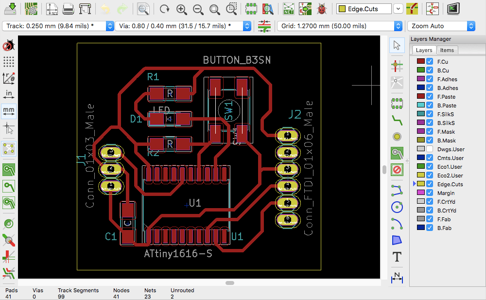
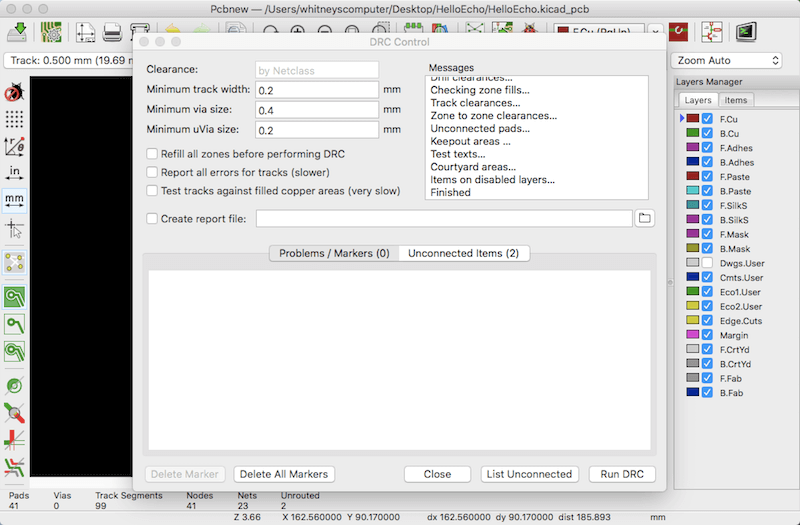
By the way, I used 0.5 mm tracks everywhere. I also changed a setting to have the minimum allowed distance between parts be 0.4 mm, which is what my bit can handle. Once I had everything mostly laid out in the PCB Layout Editor, I used the Design Rules Checker to see if I had to fix anything. I did end up having to re-route one of the GND connections (I had tried placing two tracks underneath a button, and they were too close together). When I checked the DRC control again it was clear of issues. The last part of the board design was to make a cutout shape.
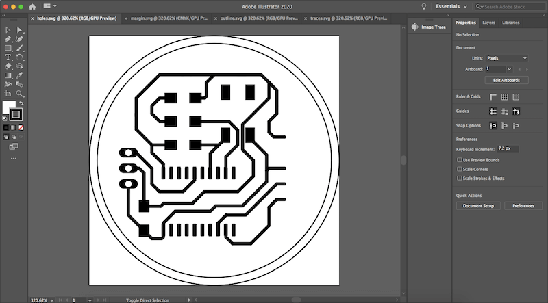
From here, I exported the layers individually, and combined, as SVG files. However, when I opened the traces up in a vector program, the footprint for the FTDI 1x06 pin header was missing. I could not figure out what to change in KiCad to fix this, and the SVG file was not convenient to edit, so I tried exporting it as a Gerber file instead.
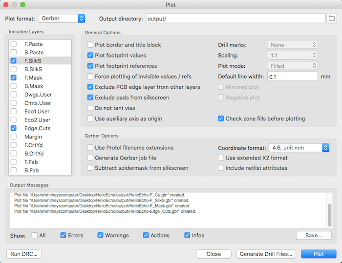
In the PCB Editor, I went to File > Plot. Here, I made sure the plot format was Gerber, and selected the layers I wanted to include. Then, I 'generated drill files' and plotted it.
FlatCAM
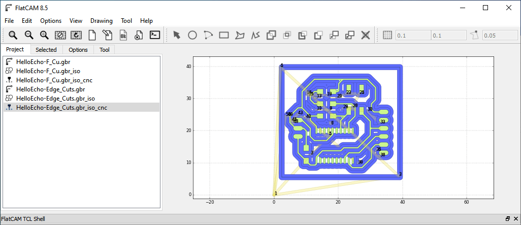
FlatCAM is a computer-aided manufacturing program for making PCBs. I was using FlatCam on one of the Lab computers, so once I had the software up and my files ready, I went to File > Open Gerber. From the folder, I chose the "F_Cu.gbr" file, which stands for 'front copper'.
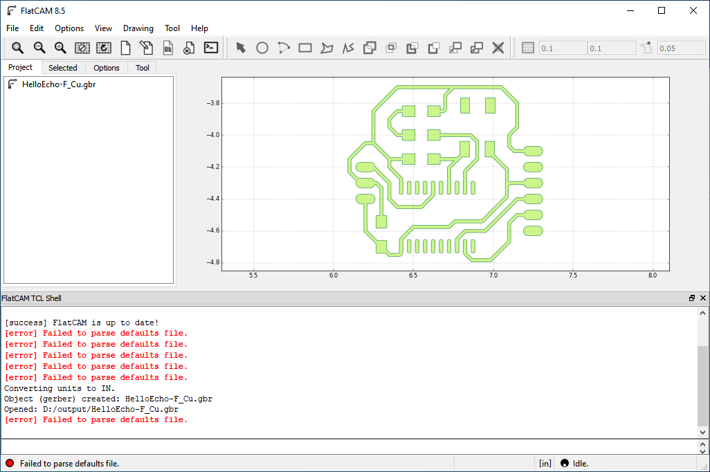
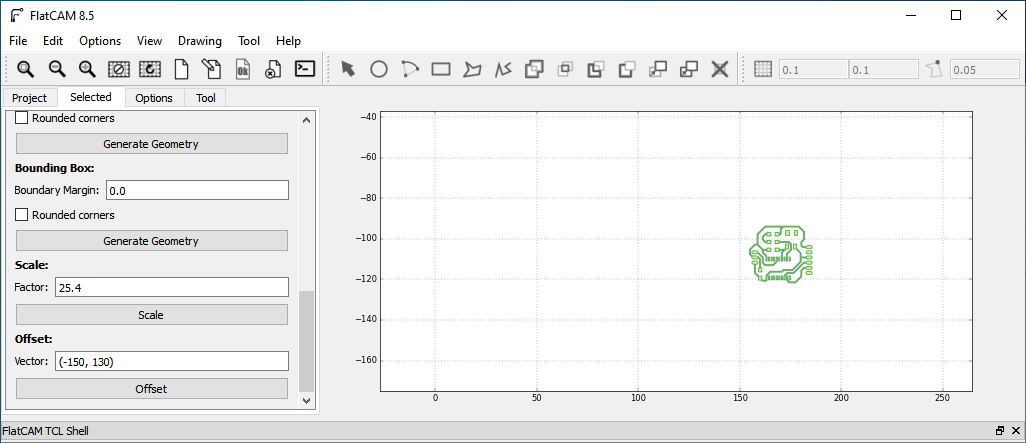
Then, under the "Selected" tab, I edited the tool diameter and number of passes, but when I clicked "Generate Geometry" something went wrong. It turns out there was a unit issue; my design was in inches and FlatCAM was using millimeters. As a result, the design was too small, and the toolpath was making a circle around the board. I fixed this problem but fixed it incorrectly (which I found out later when I went to mill my board). What I did was scale my design up by a factor of 25.4 and changed the offset to place the design back near the origin. Looking back, the red error messages should have been a sign.
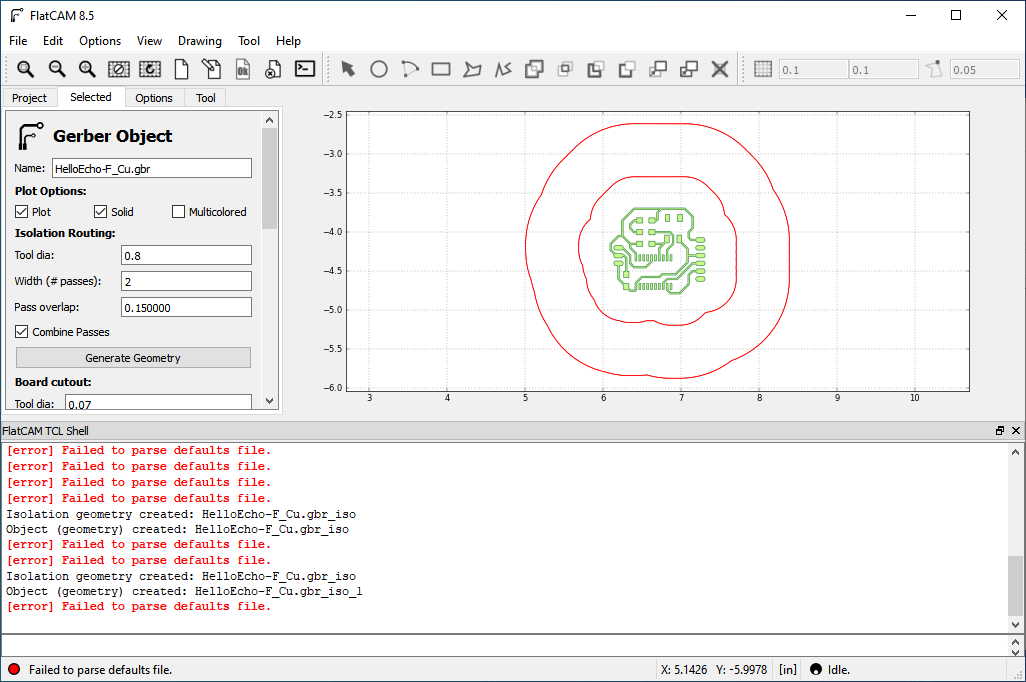
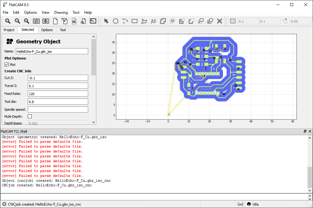
Next, I had to go back to "Projects" and select the newly generated "_iso" file. Under "Selected" I edited the Z cutting height, -0.1 mm; the feed rate, 120; and tool diameter, 0.8 mm.
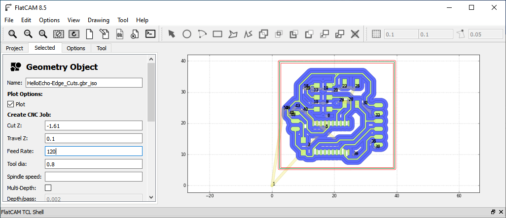
I repeated this for Edge_Cuts.gbr file, except with a cut depth of -1.61 mm, since our stock is 1.6 mm thick.
For the parts that needed to be drilled, I imported the file via File > Open Excellon. This drill file was called "PTH.drl" for "plated through hole". I used the same settings as the edge cuts file.
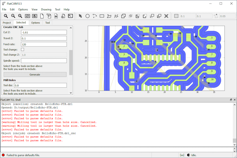
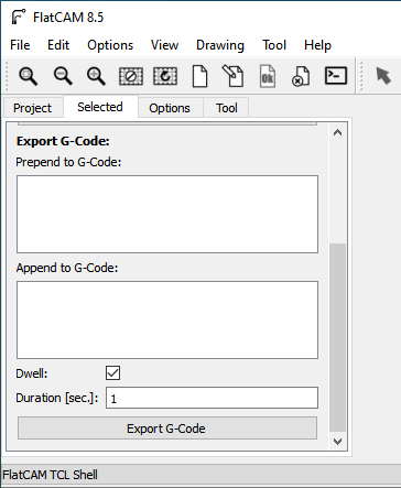
To generate the actual NC files, I selected the projects that ended with "_cnc" and clicked "Export G-Code" for each one.
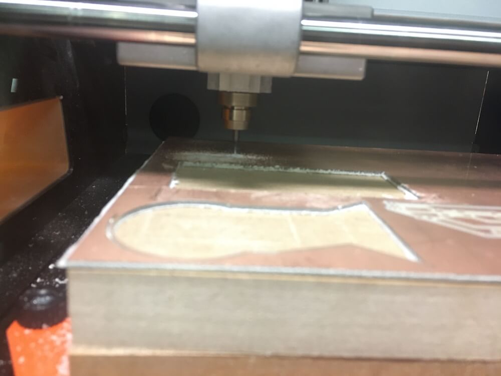
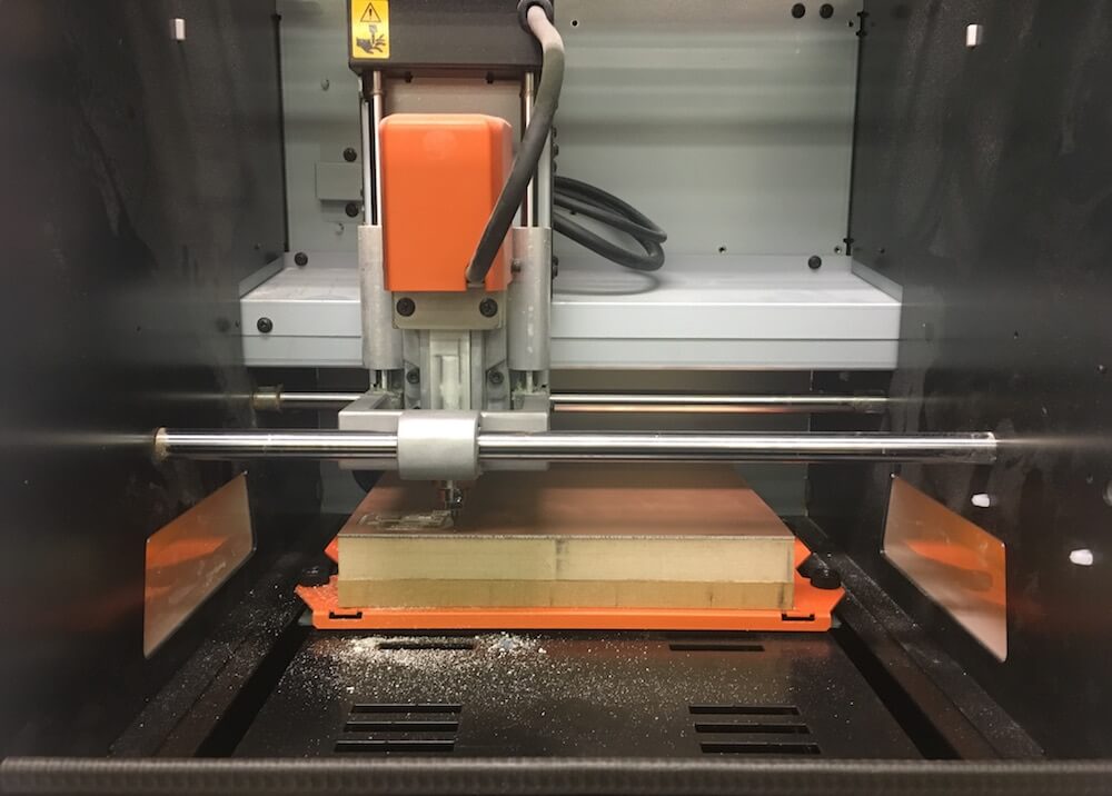
PCB Milling
I used a Roland SRM-20 to mill my board. I set up the machine, using a 1/32" ball nose end mill for the traces. (Go to Week 5 to see how I did this). I also set the X, Y, and Z origin points using VPanel. There was a small issue were the software didn't let me reset the origin points, but this was because I had different coordinate systems selected on the left and right, they needed to be the same.
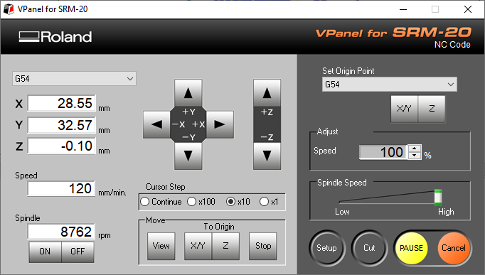
When I began my job for the traces, the machine tried to move the spindle out of range. This is when I found out that my CAM file still had the wrong units. I must have exported my KiCad design in inches and FlatCAM was reading it as something else. So, to fix it this time, instead of scaling the dimensions up, I learned how to change the project units in FlatCAM. Once that got fixed, I ran the job again in this order: traces, holes, then outline. Also, I switched over to the 1/32" end mill for the holes and outline.
It took me four tries to mill the PCB well. Here is a list of the problems that I encountered:
- The end mill was too high, possibly because the bed was unlevel, and I was milling in a corner of the workspace. Remedy = lower the Z origin a bit further.
- The copper plate shifted during a job which messed up the traces. Remedy = replace the double stick tape and really clean off the dust from the bed surface.
- The traces were too thin because the end mill was cutting too deep. Remedy = use a new section of the bed, somewhere in the center where it might be more level, and reset the Z origin very carefully to the top of the board.
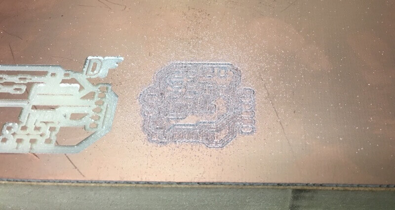
On the fourth try it worked! The traces were not too thin, and the plate didn't shift while cutting. Here is a photo comparing my 3rd and 4th attempts. Notice how the traces are almost entirely scratched off on the board on the left.
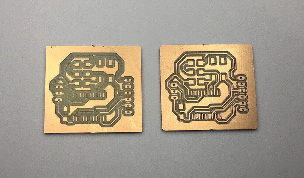
Once I had a good board, I did some post processing on it. The edges were a little rough, so I filed them down. Also, I poked the holes with a needle to open them up a bit more. There were bits of copper in between some traces, but these weren't an issue when I did continuity tests with a multimeter.
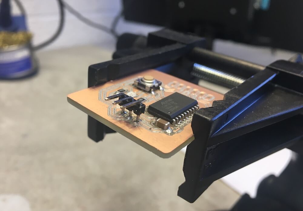
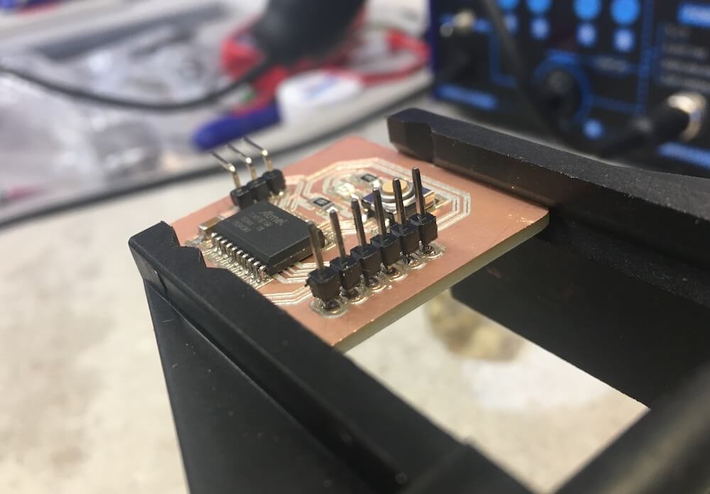
Soldering
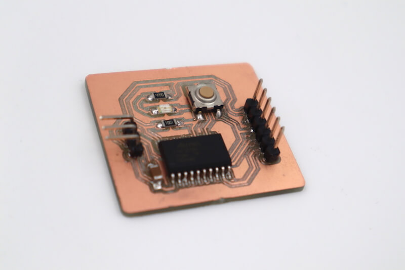
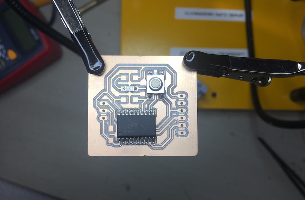
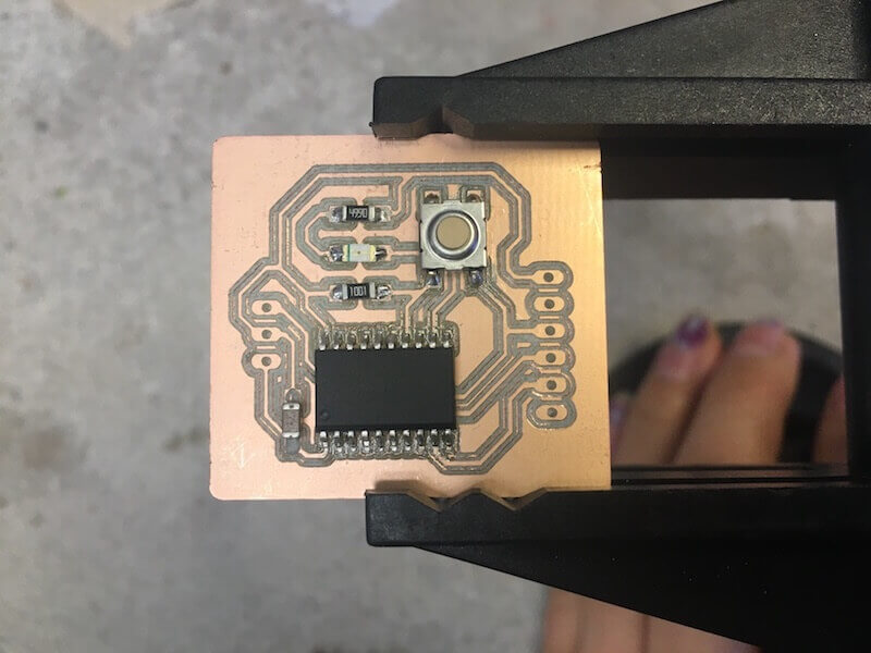
One by one, I soldered components to the board, doing continuity tests after each. Here, I added the ATtiny 1616 first, since that was the most complicated, then the button and red LED.
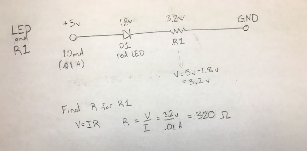
To figure out what type of resistor I needed for the LED, I looked at the product information from this DigiKey site. According to its datasheet, the red LED can handle 1.8v and 10mA. If I'm using a 5v power source, then my resistor should have a 3.2v drop. I used this info and Ohms Law to calculate the resistance for the LED. Since I don't have an exact 320Ω resistor, I used next size up, 499Ω.
Here is a complete list of the components that I used:
| Components | Quantity |
|---|---|
| ATtiny1616-S | 1 |
| red LED | 1 |
| button | 1 |
| 499Ω resistor | 1 |
| 1kΩ resistor | 1 |
| 1 uF capacitor | 1 |
| 1x3 through-hole pin (male) header | 1 |
| 1x6 through-hole pin (male) header | 1 |
For the pin headers, I soldered them onto the front as through-hole mounts.
Programming
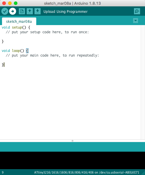
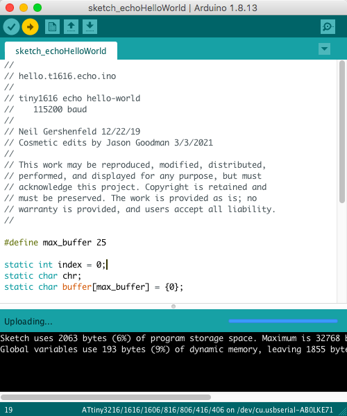
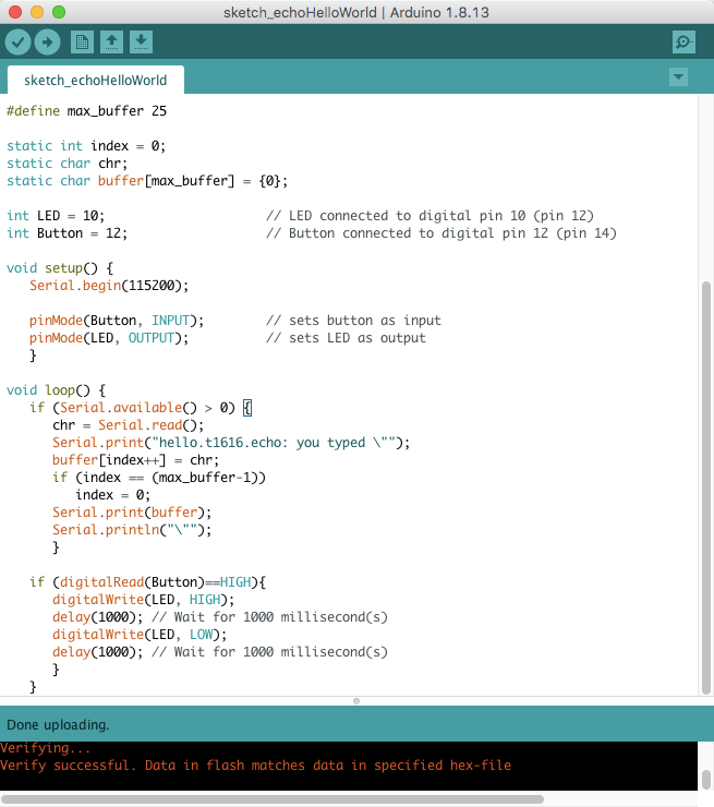
Once I had all of my components soldered, I was ready to start programming. I downloaded the Arduino software and followed some instructions, provided by Professor Goodman, on how to configure Arduino for my specific microcontroller. I had to install the megaTinyCore by by Spence Kondeto, and make sure that the correct board and serial port were selected. Then, I copied and pasted the echo hello-world code from the FabAcademy site into my sketch.
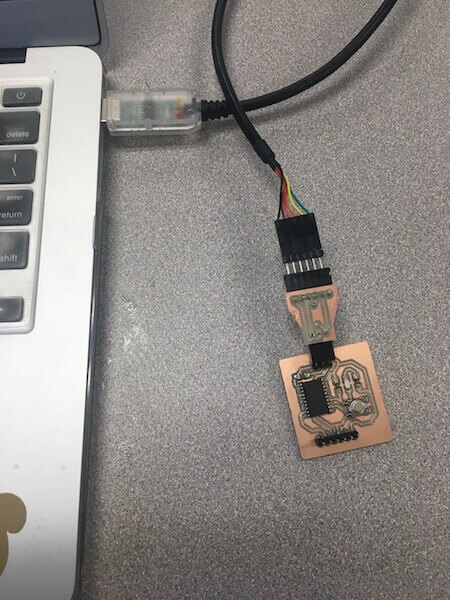
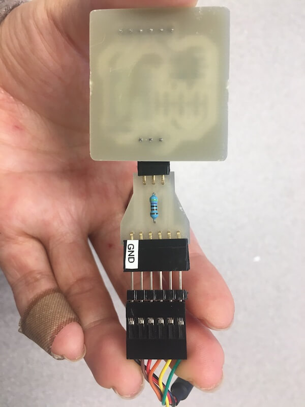
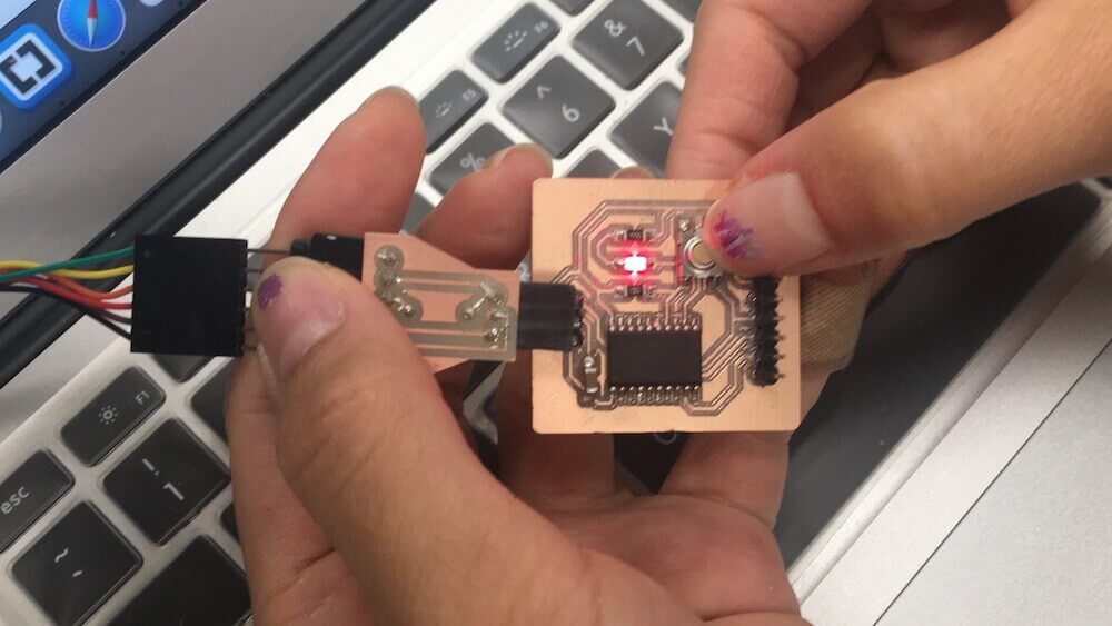
After that, I plugged my board into the computer, using the 1x3 programming pins, a FTDI USB-to-serial cable, and an FTDI to UPDI adapter. I had to make sure the ground wire was connected to GND pin on my board.
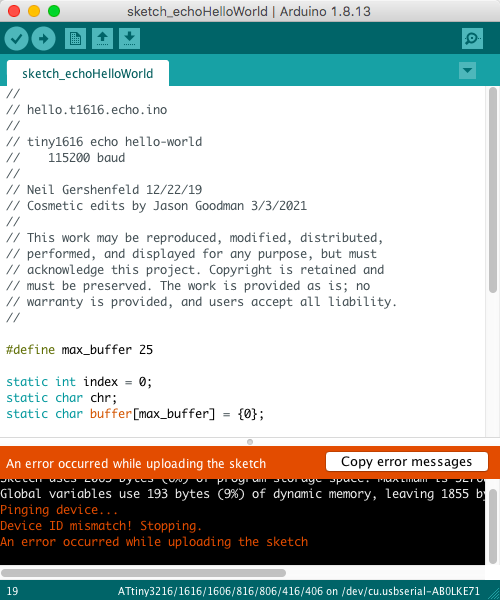
When I tried uploading my code, there were a few errors. First, there was a "Device ID Mismatch". I had needed to select the ATtiny1616 as my device under "Tools > Chip: ...". Next, there was an issue having to do with the USB port, so I tried a different outlet on my computer and that fixed it.
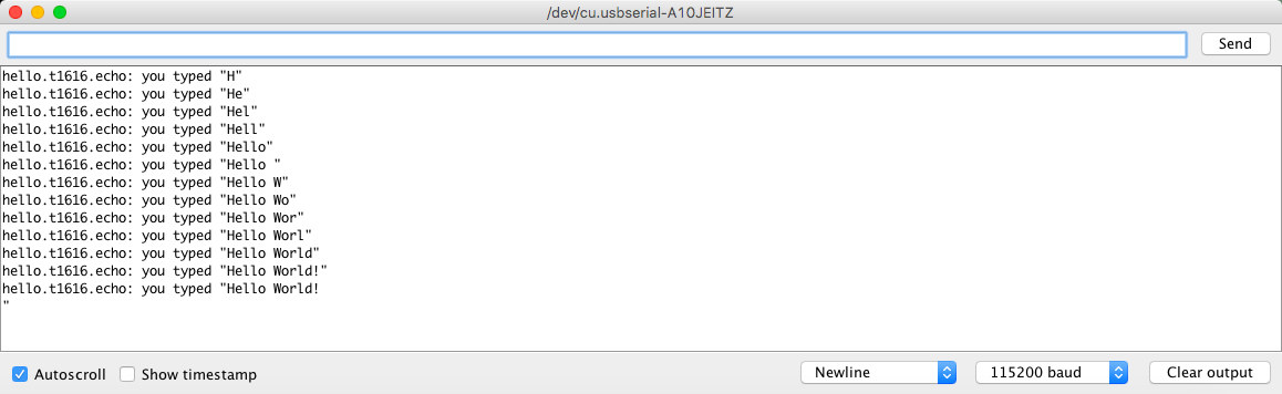
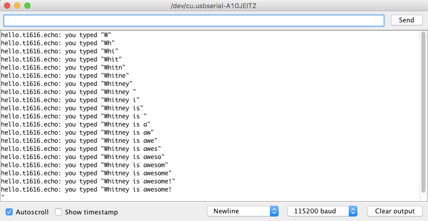
To test the echo hello-world code, I switched out the adapter, so that the USB-to-serial cable was plugging directly into the 1x6 pin headers.
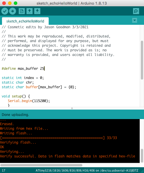
From there, I opened up the Serial Monitor, and I had to change the baud rate to 115200 to match what was written in the code, but when I typed in some text it worked!
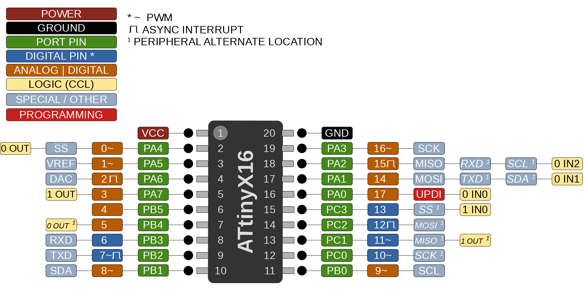
Now that I had the echo hello-world code working, I wanted to test my LED. I wrote a code to turn the LED on and off when I held the button down. I also referred to a diagram of the ATtiny1616 to figure out the corresponding digital pin number (I had initially entered the physical pin numbers for the LED and button connections, but that didn't work.)
When I switched the cables to the programming side, uploaded the code, and pressed the button it lit up!
Conclusions
This week was intense. From designing to soldering to programming, I feel like I accomplished a lot. I learned how to use three new softwares this week, and with my minimal background experience in electronics, I had to take some time to research and understand the science behind circuits boards so that my PCB would actually work, and I wouldn't blow anything up. With all of the issues I ran into I feel like I have a much better understanding of the PCB making and programming process.
Resources
- KiCad: Software | FabAcademy KiCad Libraries | Sparkfun Tutorial | Barcelona Lab KiCad Tutorial
- FlatCAM
- Datasheets: ATtiny1616 | Red LED | Button
- Arduino: Software | Tutorials | Foundations | Built in Examples | LED and button
- Programming: megaTinyCore | Echo hello-world code
- Goodman Docs: Main instructions | Assigning Footprints | KiCad to MODS to Roland PCB milling | Programming the ATtiny1616 | Workflow
Design Files
(includes schematic and PCB layouts)
Updated: March 20, 2021