Week 6 Electronics Design
Voltage, current, resistors, capacitors. That's just the beginning. Welcome to Electronics Design week!
Summary
This week about electronics design will provide a solid foundation for the rest of Fab Academy. We learn to design a PCB ourselves in designated software, then fabricate and test it.
Assignments
Group project:
- Use the test equipment in your lab to observe the operation of a microcontroller circuit board
Individual project:
- Redraw an echo hello-world board, add (at least) a button and LED (with current-limiting resistor).
- Check the design rules, make it, and test it.
- Extra credit: simulate its operation
Project management
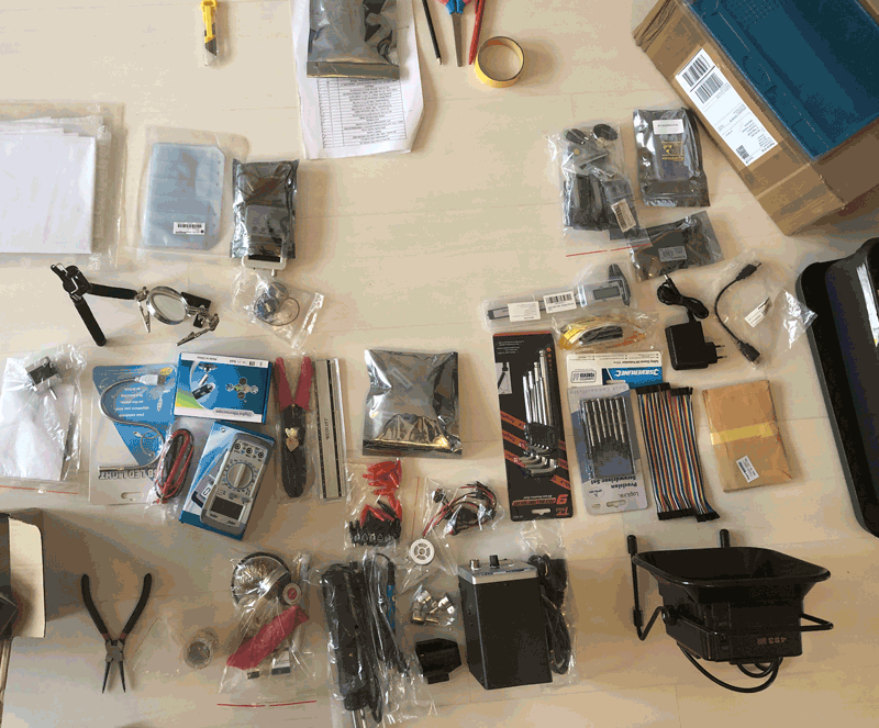
This week we finally received our home electronics kit and the desktop milling machine! This is great, because being able to mill and solder circuit boards at home will save me a lot of travel time (4+ hours per visit per day to Amsterdam).
| Spiral | Tasks | Time |
|---|---|---|
| 1 | Group assignment | 6 hours |
| 2 | Design of PCB schematics | 16 hours |
| 3 | Unpack Fab Academy electronics kit and check if it’s complete | 3 hours |
| 4 | Create home lab area | 1 hour |
| 5 | Build, program and test Fab Academy milling machine at home | 8 hours |
| 6 | File preparation and milling | 8 hours |
| 7 | Soldering | 4 hours |
| 8 | Programming and testing the board | 5 hours |
Let’s get started!
This week’s results
And, happy news, because our Fab Academy electronics kit arrived!
And the CNC3-3018Pro, a small milling machine for our home lab during the pandemic. Check out the assembly process:
In retrospect this week was extra challenging for me, because of a setback in getting the KiCad library on Mac, additional time needed to build the milling machine, and missing components in the home electronics kit.
First I noticed there were missing parts for the milling machine. If I would order them online they would not arrive in time. I solved this by contacting a local vocational school. Luckily they opened their doors and allowed me to mill the PCB in there. Because this is a rural area, I was very surprised by their advanced machine, a UV printer. It was a cool experience to learn about other ways to make PCB’s.
Then a second problem arose, because not all components for this week’s assignment were included in the Fab Academy electronics kit. The vocational school offered to help, but unfortunately also didn’t have these specific components. It took extra time and effort to travel to Amsterdam, just for soldering the board. But it succeeded!
The missing components needed for week 6 are:
- FTDI
- UPDI
- Button
- Phototransistor
- Smaller diameter solder wire (1 mm is too big for precision work, at least for me)
- Nice to have/more safety: soldering iron controllers (holder)
- Nice to have/more safety: brass sponge holder
Milling machine:
- Milling machine end stops
- Acrylic bed protection with inlay for sacrificial layer + copper plate
- Sacrificial layer (larger copper plate)
- Nice to have: Henk’s turbo end mills for Fab Academy-worthy results
Hopefully they can be added to the inventory for future students. Now let’s get on with this week’s assignment!
Electronics 101
Because I’m new to electronics, I’ll start with an overview of basic principles, equipment and tools, components and schematics. This section is concluded with the group assignment.
Basic principles
Direct current goes in one direction.
Ohm’s law = R = V / I
V = R x I
- Current (I)= amount of electrons coming through
- Voltage (V)= push of the current
- Resistance (R)= measured in ohm.
Current
- No slope = no motion
- slope = motion
- obstacle = for example by a resistor, = motion with control
Voltage
Push of the current.
Resistance
Can be measured with a multimeter. Unit of measure = ohm.
You can’t measure components that are already on the circuit. Because it is measuring everything around it too. The traces create noise.
Power
Power (Watts)= important. When the power is higher than listed on the datasheet, the device will burn.
P = V x I
P = (R*I)*I = R*I^2
Circuits
Resistors or batteries can be wired in series or parallel.
Example: Series: 18V In parallel: still have the same volts, but more amperes. 9V
A fuse (can handle amount of current through a lamp) = ‘zekering’ in Dutch.
Sustainability
Lower voltage = losing less power = less waste
Measurement tools
When working with electronics, certain tools will make your life easier. At Waag, Henk shows us the tools available:
- Multimeter is a tool to measure two or more electrical values, for example voltage, current and resistance. This is how you use it:
- Set your multimeter on DC.
- Beforehand, you need to have an idea of the range of your voltage. First look at the voltage of the object. This will give a direction.
- Set the switch to 2V, 20V or 200V, depending on your estimated value. Never set it to 1000 or 700 volts.
- Measure the value.
-
Unity multimeter with clamps: tool to measure the fields of the wire.
-
Big red multimeter can be connected to the computer. Less accurate.
-
Miniware Digital tweezer to measure small components. They are very precise and manufactured in Shenzhen. According to Henk you can buy them blindly, they are of good quality.
Components
Ground
VCC
Capacitor is a form of energy storage, but it’s not a battery. The current doesn’t flow through the capacitor. It’s there to remove noise from the signal. The measuring unit is in Farads.
There are two types of capacitors:
- Non-polarized
- Polarized (can handle more storage)
Usage of a capacitor: for example with microcontrollers. They generate noise. When placed in between the microcontroller and ground, peaks will be leveled out by the capacitor.
Second example: LED. First charge the capacitor, then when it’s full, the current will go to the LED. Now it’s brighter. When you turn off the battery, the LED will continue to shine and slowly turn off. A delay is created in between the moment of removing the battery and turning off the LED.
Caution: it is dangerous to have a capacitor in a charger, for example laptop charger.
Resistor
Microcontroller. In this case an ATtiny44-SSU.
Header pins. We’ll use the UPDI pins.
Crystal Resonators are a critical part of the microcontroller circuits. They help provide a clock signal. A clock is a particular type of signal that oscillates between a high and low state and is utilized like a metronome (instrument) to coordinate actions of circuit. The clock pulse is the frequency. New ATtiny’s have a resonator built in.
Schematics (how to read it)
Design principle:
- plusses on top
- minus / ground on bottom
Components: R Resistors C Capacitors L Inductors S Switches D Diodes Q Transistors U Integrated Circuits Y Crystals and Oscillators
GND = 0V Ground VCC = 9V (current) Battery
Resistor in schematic (R1), and underneath it the value of the resistor. This makes it easy for yourself to build your PCB at the end.
Voltage Nodes
Nets & Junction
- Green lines are nets.
- When there is a a dot on it: lines are connected
Sometimes net names (a wire between two connectors) are connected with tags/labels. Diagonal lines are internal connections.
Ground is twice on the board, they are connected.
Simplest circuit + LED
- they are “non-ohmic” devices
- creates a “voltage drop”
Voltage Forward (Vf) = you need to push 1.8 voltage, if you
There is an LED calculator for designing a circuit. You can make a schematic or a wiring diagram.
[image]
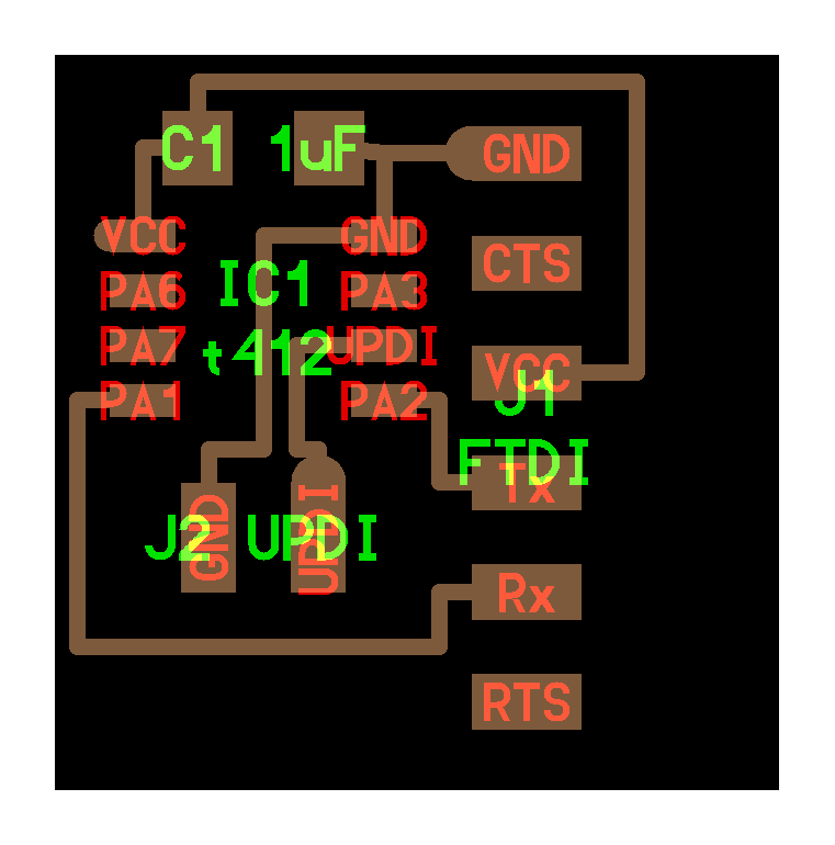
Hello Echo board
Components
- capacitor
- resistor
- headers (header pins - we’ll use the UPDI pins)
- Microcontroller: ATTINY44-SSU
- pin 8
- pin 2/3 are XTAL
Three images:
- Schematic (functions of pins are described in schematic)
- Design Board
- Traces / interior for milling
- Image of fabricated board
XTAL - timing/clock
Pin to reset the IC
Through Hole Technology (THT) - colors of lines tell you the resistance.
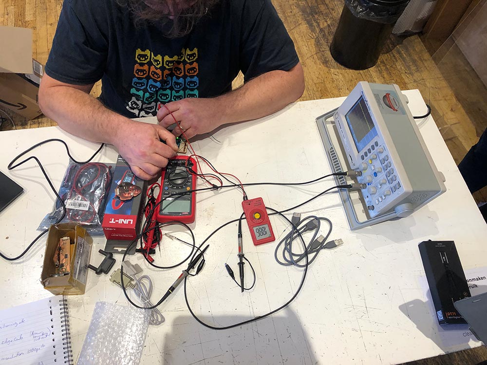
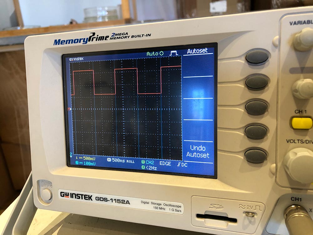
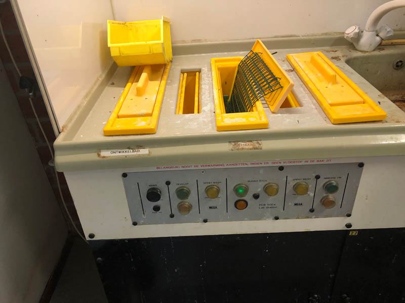
Measure something in the lab!
Measure voltage
Oscilloscope
Board design: Hello World
In the section below a Hello World board is redrawn from the example board on the assignment page. The links are:
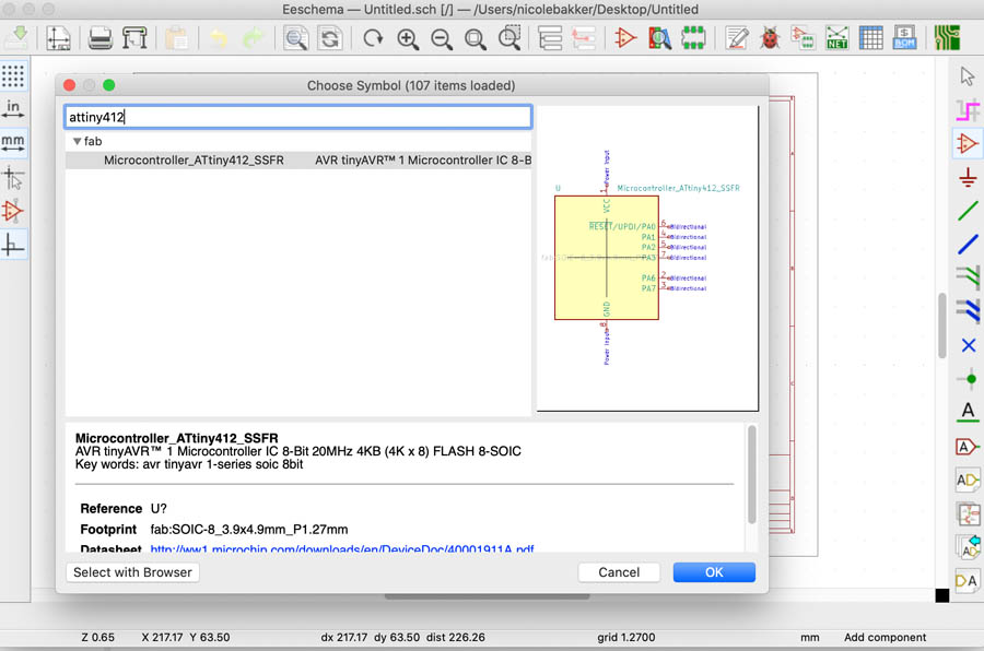
The following components are used:
- ATtiny412
- UPDI
- FTDI
- Capacitor 1uF
In addition to the board above, we will add:
- Photoresistor (input device)
- Button
- Green LED
- 2 resistors (5.99k and 10k)
Installing KiCad
Download the Current Version: 5.1.9 from KiCad. Next, download the Fab Electronics Library for KiCad. Clone or download the whole library and follow the installation instructions provided on Gitlab:
- Clone or download this repository. You may rename the directory to fab.
- Store it in a safe place such as ~/kicad/libraries or C:/kicad/libraries.
- Run KiCad or open a KiCad .pro file.
- Go to “Preferences / Manage Symbol Libraries” and add fab.lib as symbol library.
- Go to “Preferences / Manage Footprint Libraries” and add fab.pretty as footprint library.
- Go to “Preferences / Configure Paths” and add variable named FAB that points to the installation directory of the fab library, such as ~/kicad/libraries/fab or C:/kicad/libraries/fab. This will enable the custom 3D shapes to be found. The 3D shapes project has just started and most of them have to be populated still.
On Windows, KiCad automatically links to its own libraries. On Mac, it was a little painful because it doesn’t load the libraries automatically.
For Apple users, download and install common libraries from Kicad:
- Schematic symbols
- PCB footprints
- 3D models
Symbol Libraries: click on the folder to add a new folder. Navigate to the path described above. Select one .lib file and press shift to select all of them in this folder. Hit open. All symbol libraries will be added. Do the same with all the .pretty files in the Footprint Libraries. Next, Configure Paths by linking to the entire folder.
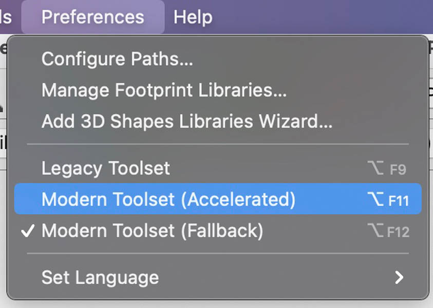
Even though I set up the common library multiple times, and communicated with other students who had the same problem on Mac, it still didn’t show up on my machine. That’s why I eventually decided to set up Bootcamp on my Mac and run KiCad on Windows.
Update (May 2021): I found the cause! It is a very simple setting, just change the Modern Toolset to (Accelerated).
Now you’re ready to start designing! A KiCad tutorial can be found here.
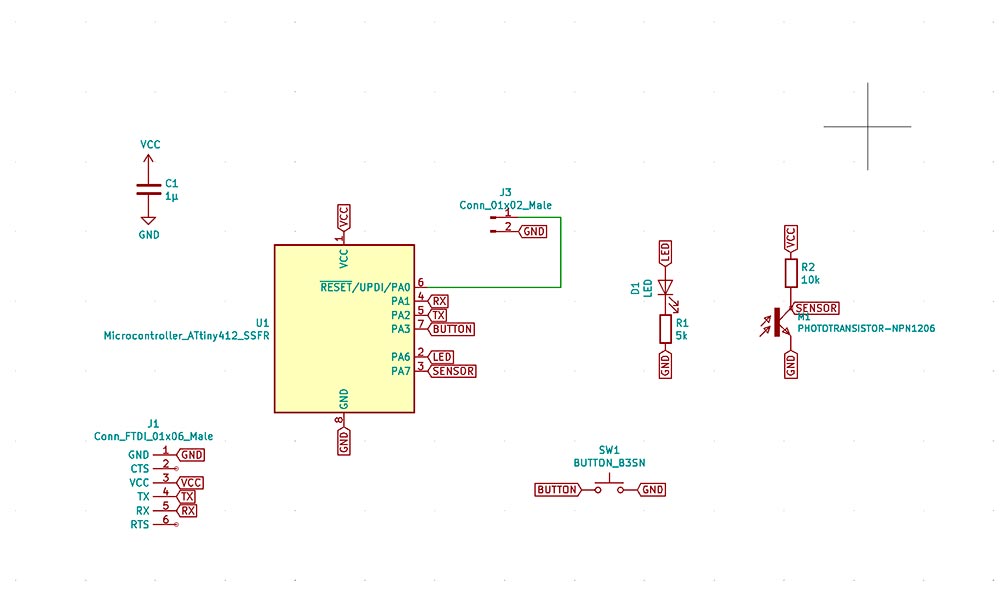
Draw the schematic in Eeschema
In the navigation bar on top, click the first icon for the Schematic Editor.
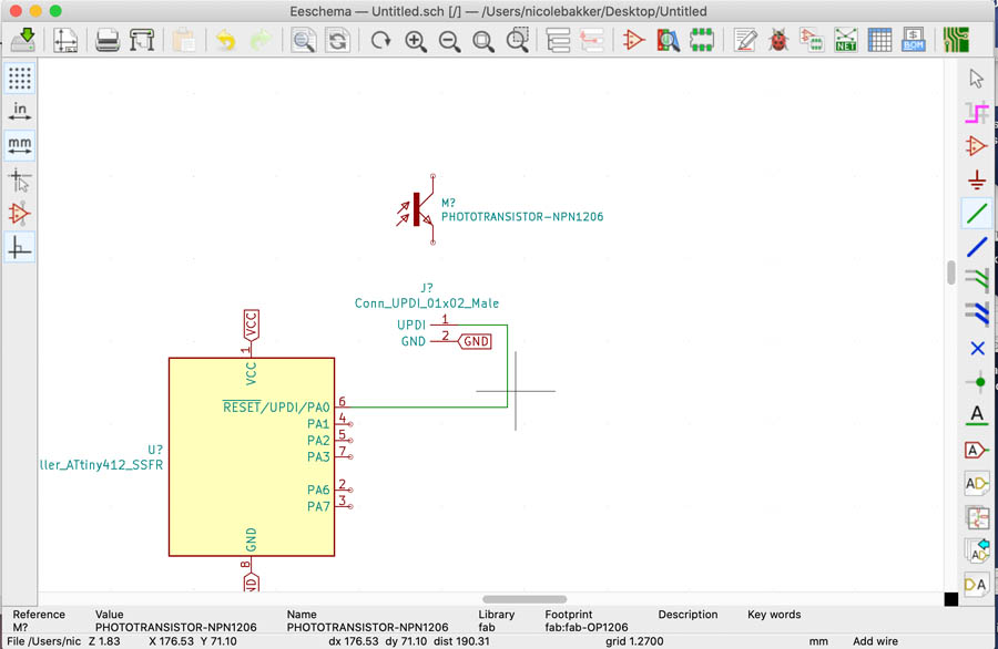
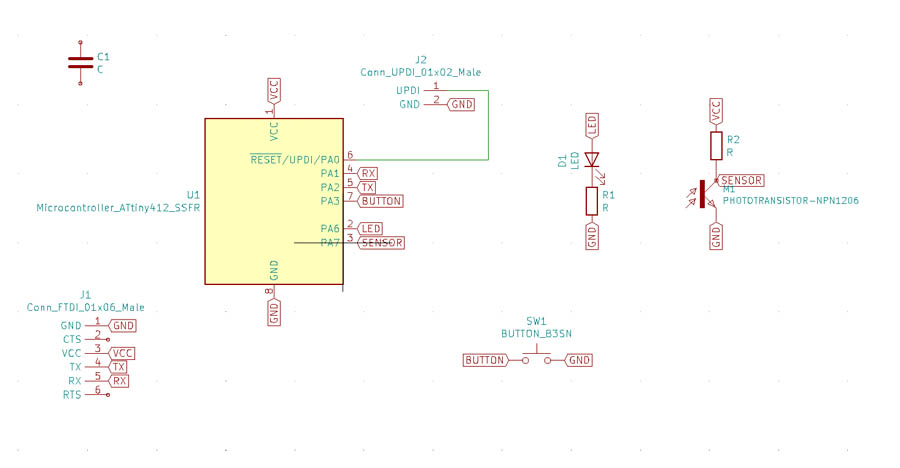
Eeschema opens up in a new frame. Next, collect all components you need with place symbols. The result of the schema:
Locating buttons in interface:
- Place components (3rd icon in right menu)
- Add power symbol (VCC) (4th icon in right menu) and add ground (GND)
- Wiring:
Place Wire(5th icon in right menu).
Adding components:
- From common libraries: GND and VCC
- From fab library: ATtiny412, FTDI, UPDI, Capacitor, Resistors, green LED, photoresistor, 6x6 mm button.
Connections:
- Always draw VCC above GND. And on all components GND below.
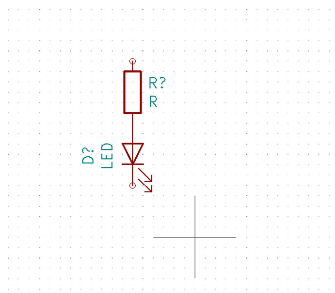
- LED: connect to resistor
- Capacitor: connect VCC above, GND below
Tags:
- LED tag / LED / Resistor / GND tag
- VCC tag / Resistor / Phototransistor / GND tag
Use this icon to add components:
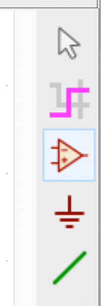
Click on the canvas and search for the component in te fab library.
The component will then show up in the canvas. In KiCad it’s possible to work with hotkeys. This speeds up the design process significantly.
- Rotate component: select + R
- Move component: select + M
- Select single component: select + right click ‘move’
- Option + M = µ sign on Apple
It is also possible to rotate a component or footprint in an angle of let’s say 45 degrees instead of 90. Select the component, right click and Edit. In the menu, you can enter a custom value. Or simply select the line or component and type E. That will open the properties panel.
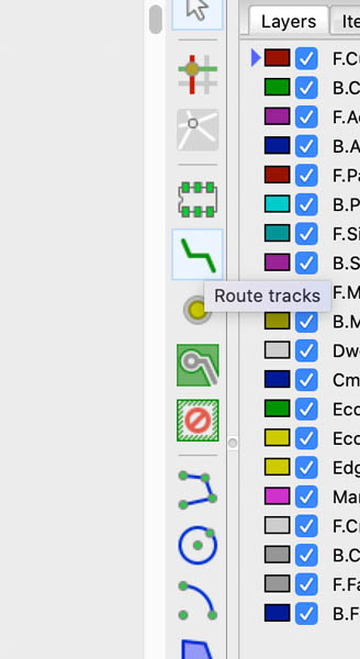
When all components are there and you’re happy about their position on the canvas, you can route tracks between components with this icon:
For example, in between the UPDI connector and the ATtiny412.
Another way to connect components is to add labels. This can be found on the navigation bar on the right. When typing the component, make sure to use exactly the same words. The labels are also sensitive for uppercase and lowercase letters.
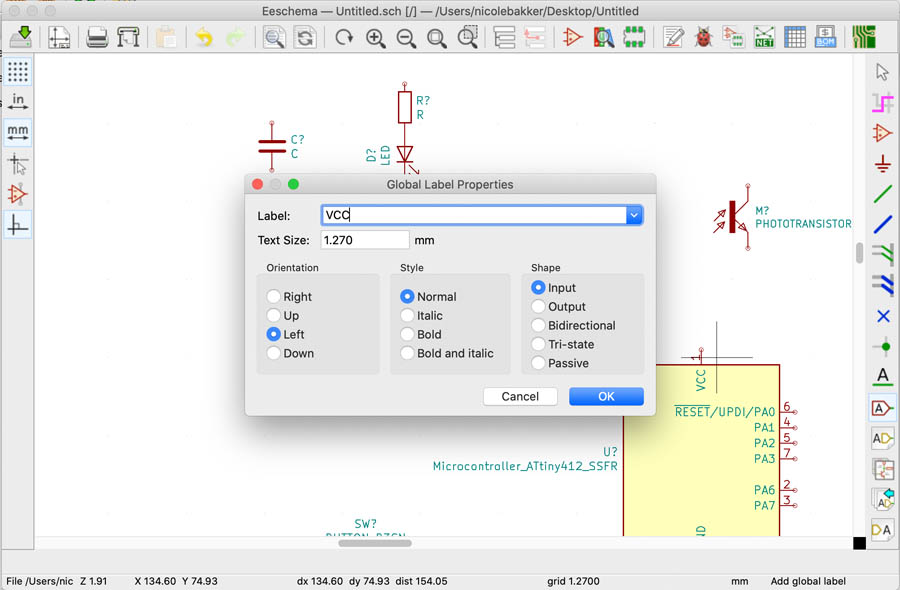
VCC is added to the top of the ATtiny412.
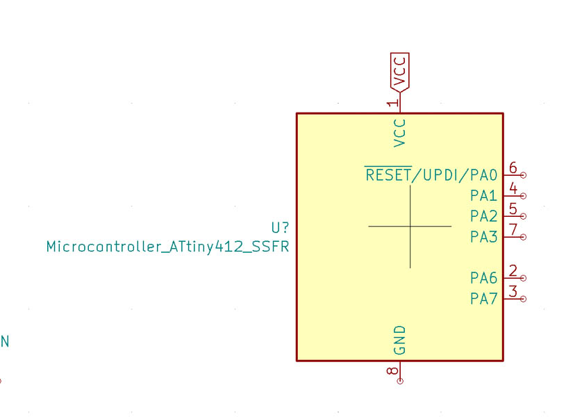
And do this with the rest.
Special shapes EdgeCuts = layer for circles etc.
Add properties to the components
In the canvas, you can’t see what the values are of for example a resistor. On an object, click Symbol Properties.
- Stand on resistor 1 –> right click –> Properties –> Edit Value –> 5k (this is a lot, but Henk doesn’t care)
- Resistor 2 (phototransistor)–> 10k
- Capacitor –> 1µ
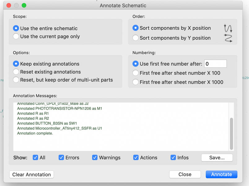
Annotation and create PCB Footprint
If there are question marks in the components, it means they are not annotated yet.
Click Annotate Schematic Symbols (top navigation bar). This will automatically link the components.
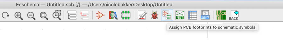
Next, Assign PCB footprints to schematic symbols.
Just click OK because they are all assigned in the previous step.
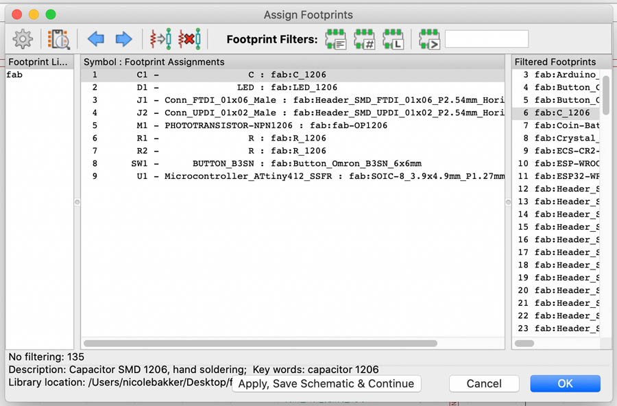
Now you can continue.
Generate netlist
Netlist will put the connections between the components. will keep track of it. To say: what connections are in between components. In KiCad version 4 you still have to do this manually.
In the navigation bar, click on the Generate netlist button.
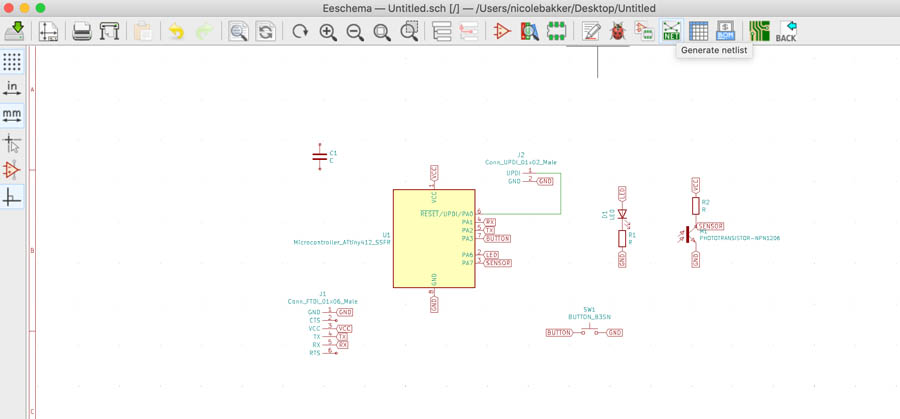
This opens a window. Click Generate Netlist.
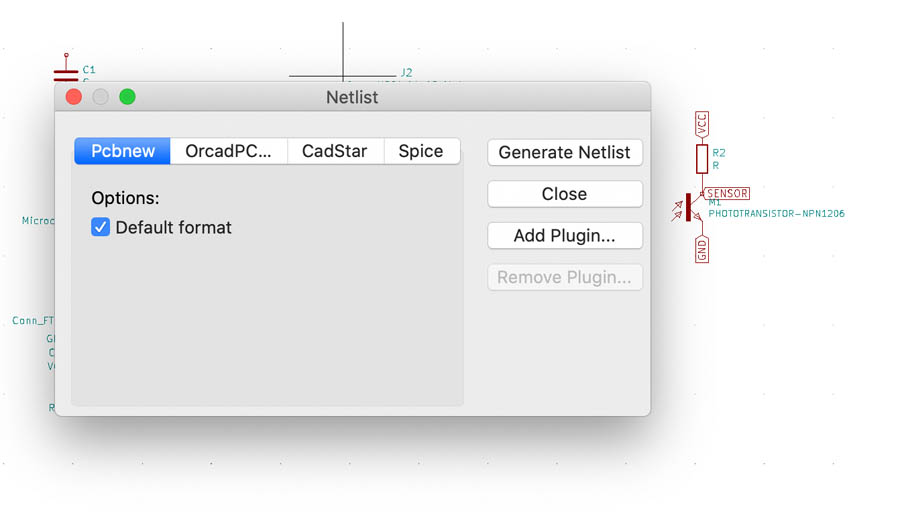
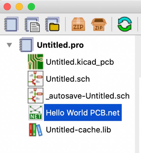
The Netlist will be added to your directory.
In version 5 of KiCad, it’s done for you. For example, if you want to rotate a component, you can do it in PCB Editor, and it will automatically update the netlist. So download or upgrade to version 5!
Bill of Materials
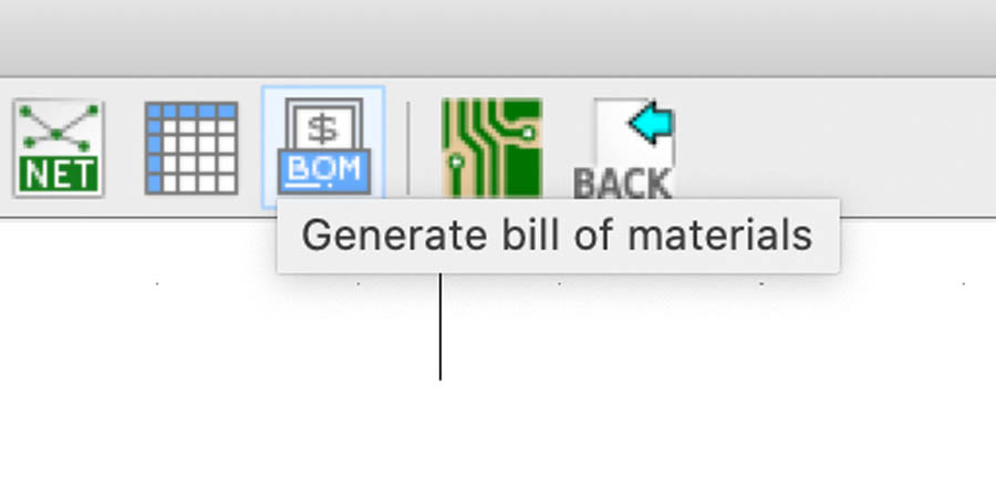
Click Generate Bill of Materials in top navigation bar.
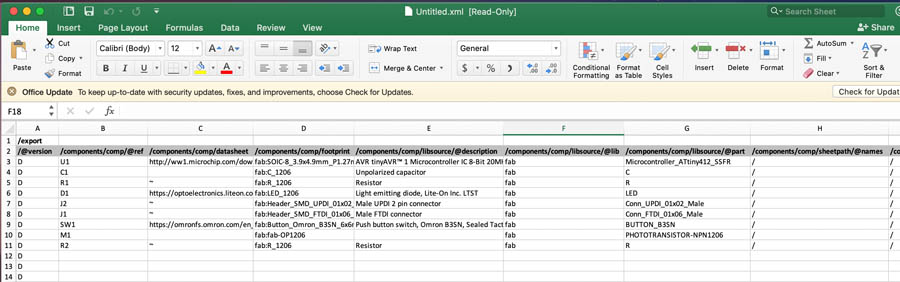
A list with plugins shows up. Because I’m a noob at this, I select bom_csv_grouped_by_value in the hope its readable in Excel.
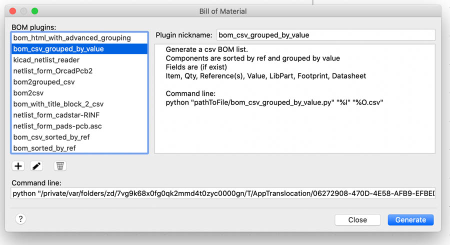
This Python script generates a csv BOM list.
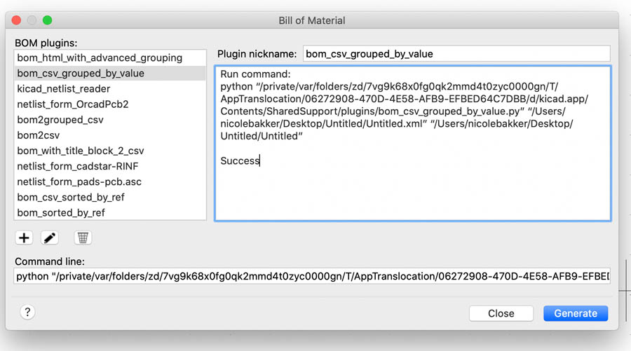
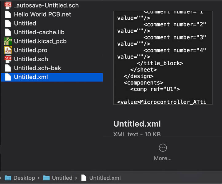
The excel file shows up in my directory.
Success! The bill of materials is included.
PCB Layout Editor
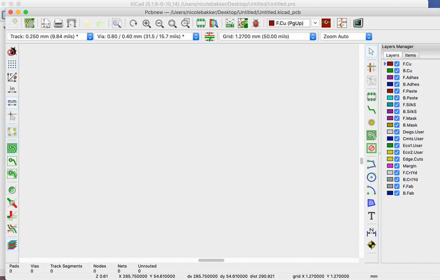
In the main KiCad screen navigate to PCB Layout Editor.
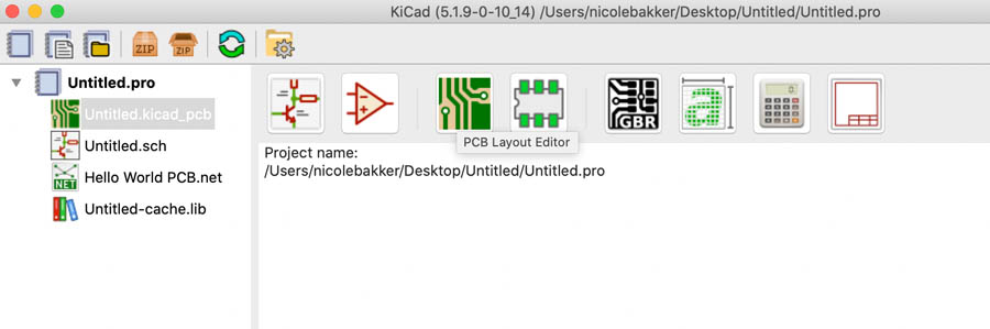
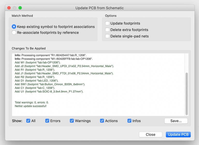
To import your schematic, click Update PCB from Schematic....
Click Update PCB. If it loaded the netlist successfully, it shows the following message.
It will then show a black screen with your components. Importing the schematic in Pcbnew was troublesome on Mac. On Windows, it went seamlessly.
An important first step is to set the design rules of the PCB.
Navigate to File, then Board Setup and the tab for Design Rules. There are no vias or holes in this board, we’re making a one-sided PCB. The minimum track width = 0.4 mm. And clearance = 0.4 mm.
We’re going to draw two layers:
- F.Cu = front copper layer (red layer)
- Edge.Cuts = for the outline (red layer)
- Margin (magenta layer)
We also use a margin around the EdgeCuts–> look up documentation of students from previous years.
Start with F.Cu.
Get rid of the white lines. go to route tracks and connect the components.
White line = redsnest Red = copper traces ()
Nice tool in kicad: Inspect –> specify the margins of traces and spacing. makes sure you don’t
Is there an algorithm that can found the most optimum route? Yes, it’s called Outer Router. It works horribly. There even is an ‘Never trust the outer router’ T-shirt ;-)
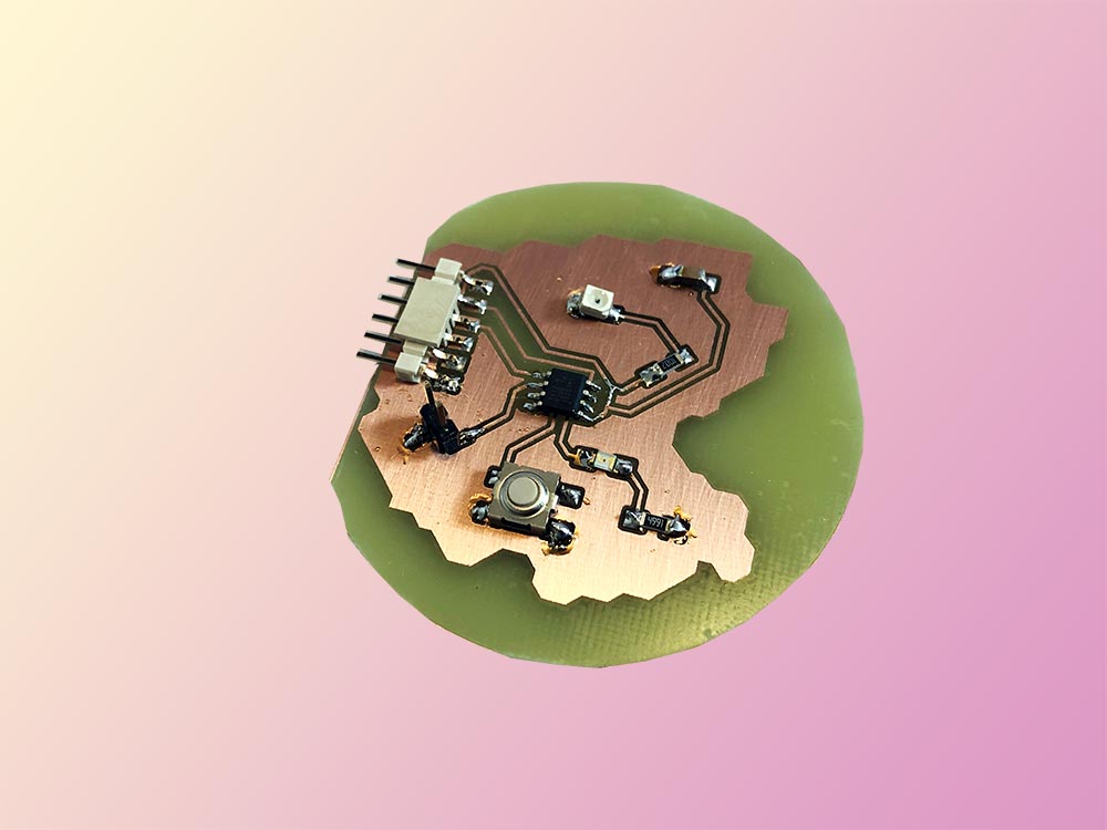
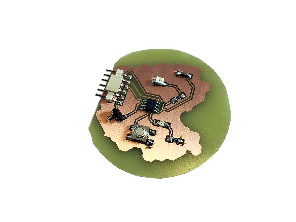
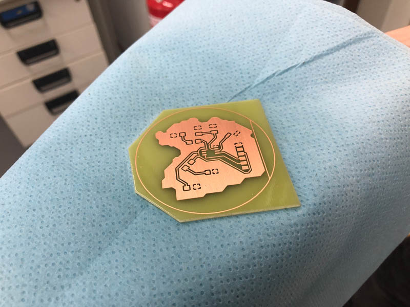
I decided to draw the outline of the province of Friesland.
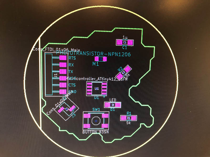
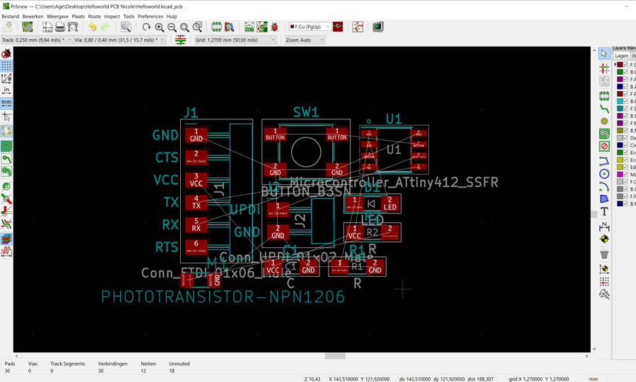
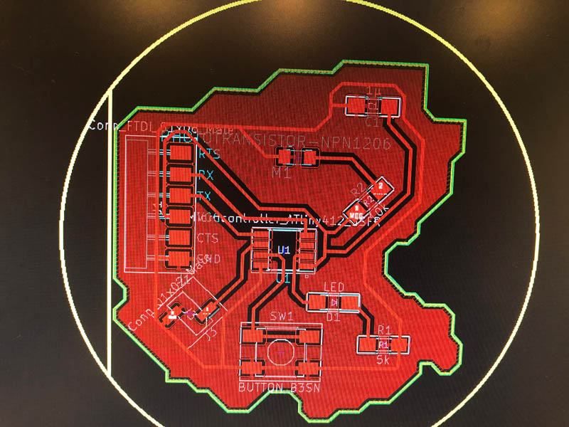
This is the final PCB design with all traces:
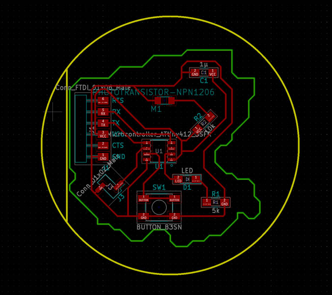
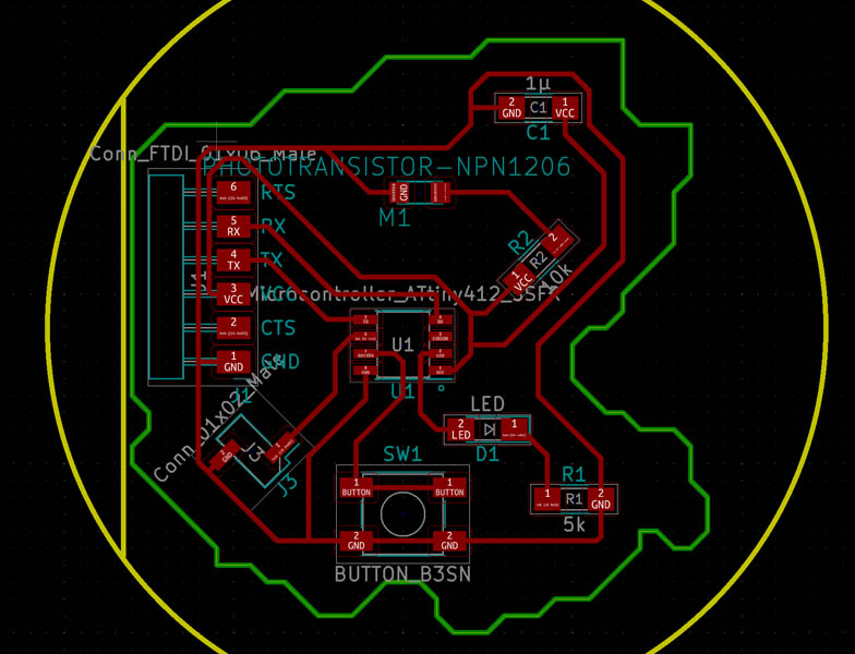
A close-up to see the orientation of the components.
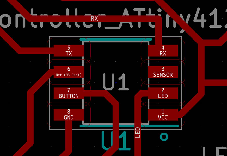
And a close-up of the ATtiny412.
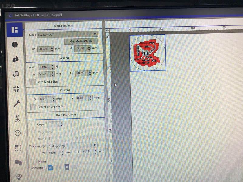
Exporting SVG
File –> Export -> SVG..
F.Cu = front copper layer Edge.Cuts = for the outline (cut) Margin = for milling
Set Print mode to Black and white. SVG page size to board area only.
Export. It shows the path where it’s exported.
Resolution of 1000 pixels. This is what you need for mods.
Then, MODS time! The resolution of an SVG is really low in mods.
UV printing process
Because it takes 2 hours to travel to Amsterdam, and Waag being closed during the weekends, I started to look for lab access at facilities in my hometown Leeuwarden. Luckily, the department of engineering and technology at the vocational school Friesland College welcomed me! Thanks to Dirk and Renze for providing access to the fabrication hall and guidance with the machine.
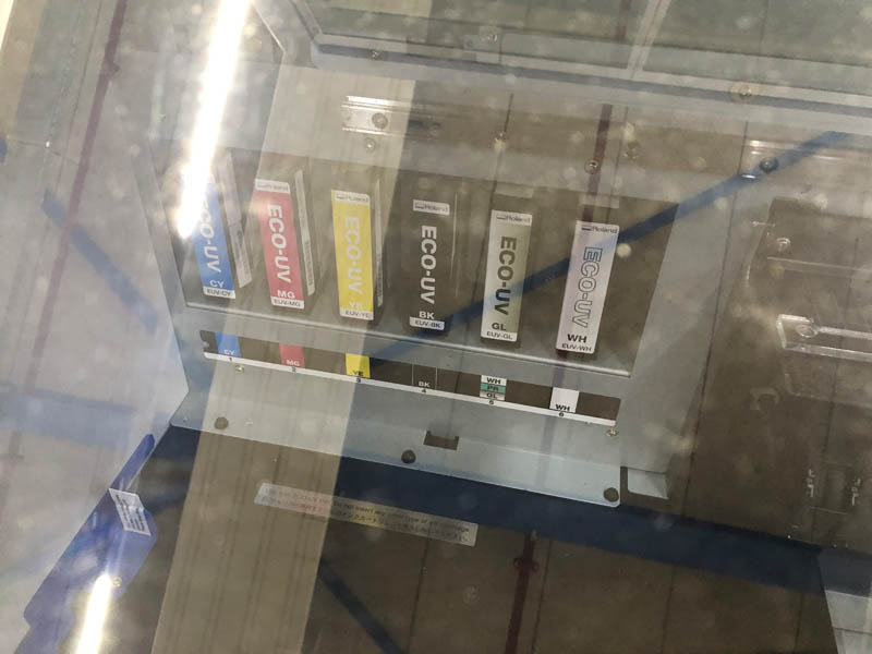
The machine in this lab is a Roland VersaUV LEF2-200 flatbed printer. I am quite impressed by it.
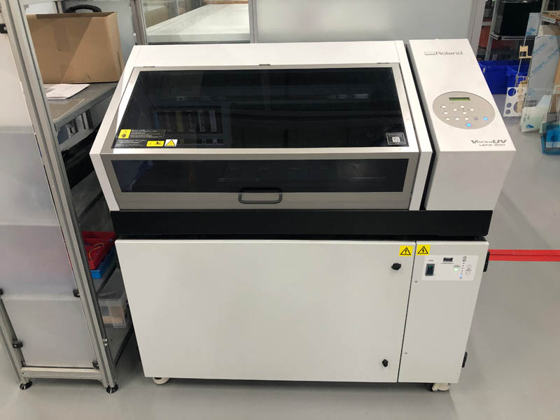
It has large cartridges.
File preparation in KiCad
In addition to the steps for milling PCBs as described above, we need to do some additional steps in KiCad.
Common Ground
Click Add filled zone for automatically linking the common ground. What is this and what does it do? In this case: common ground are the parts that will not be ‘milled’ away and remain conductive copper. With this method you don’t need to wire. The ground trace disappears, and everything around the circuit board is ground :)
Traces
Watch out: there will be a hydrophobic effect when the distance between the traces is too small.
Edgecut circle = line thickness 0.39 mm
Export pdf
The next step is plotting to pdf. This can be done in KiCad.
Click Plot then PDF and deselect all Layers You only keep the F.Cu and Edge.Cuts layers. In settings, set the drill marks: small.
Mirror image of PCB is not needed now.
File preparation in Illustrator
Now we need to crop the image. Open Adobe Illustrator and open the pdf. In the top menu bar, navigate to Object, then Artboards and click Fit to Artwork Bounds.
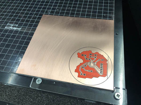
Add color and texture if you want. With the UV printing technology it is possible to print PCB’s with color, even with texture. What would be better than a Frisian Flag design?
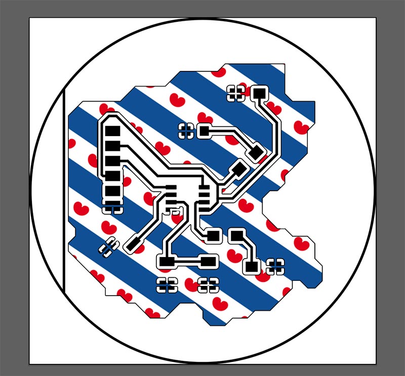
Due to time constraints, I decided to first print the initial design without texture.
To export the file, safe as pdf.
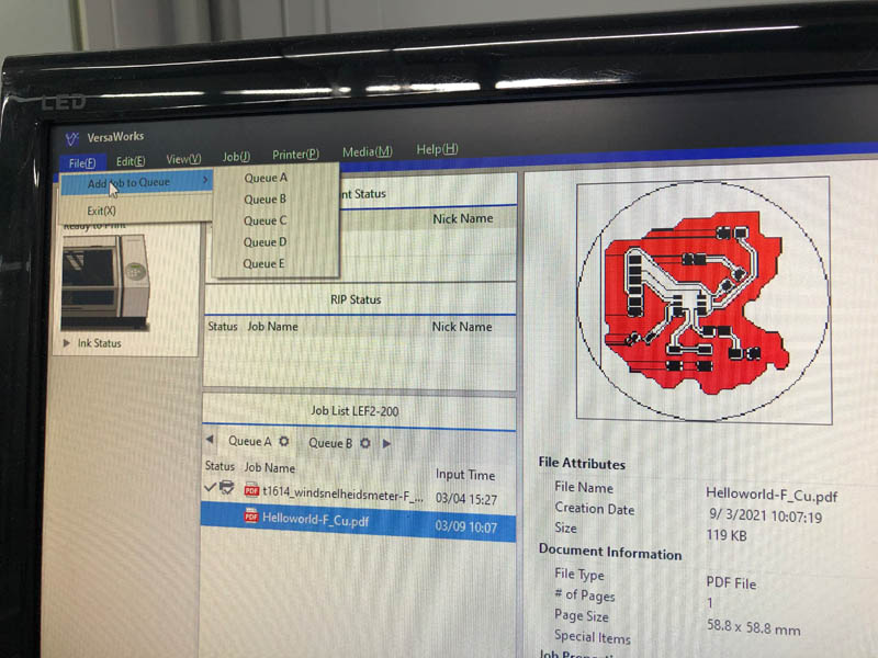
Versaworks file preparation software
Versaworks is Roland’s print management software that comes with the printer. In the software, Open File and select the pdf. The file will show up. In the canvas, move your object 1 mm from the sides (position x and y axis). Otherwise it will not print nicely.
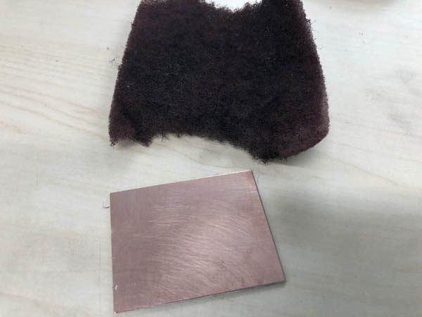
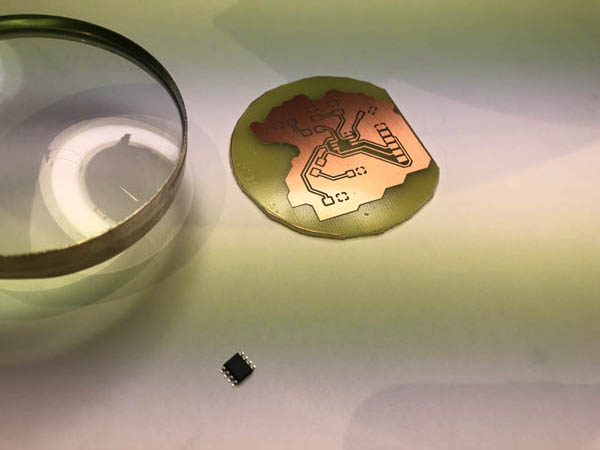
Copper plate printing steps
Take a copper plate and use Scotch-Brite for grease removal & better adhesion of the print. Scratch the copper surface a bit.
Clean the copper plate with water, make sure not to touch the copper side.
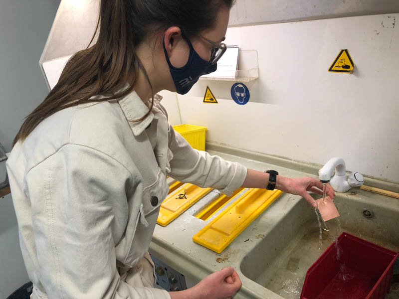
Dry the copper plate with a paper towel and remove remainder parts.
Place the plate on printing bed Roland, make sure it touches the corners. First press it to the x-axis, then to the y-axis. Next, with a paper towel, softly press pcb into the bed (z-axis).
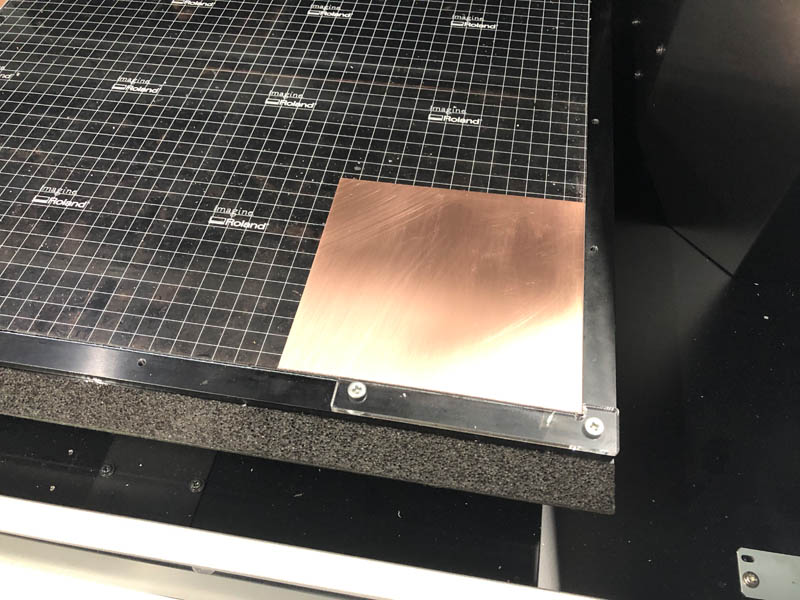
Software: send to printer (bed leveling is set by lab manager)
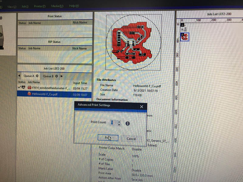
Processing job.
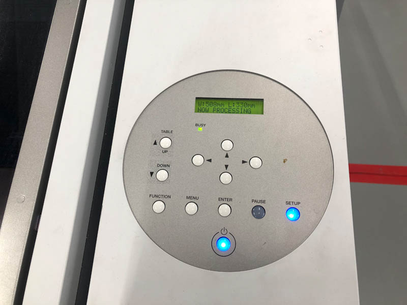
Printing job starts.
It deposits ink. The total printing time of this PCB was ony 4 minutes. A general principle is less copper = less printing time.
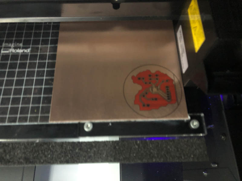
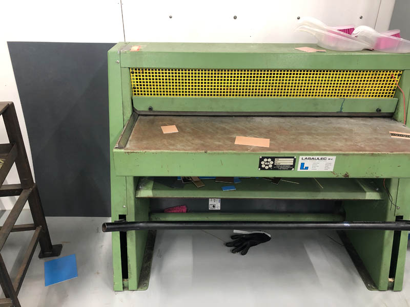
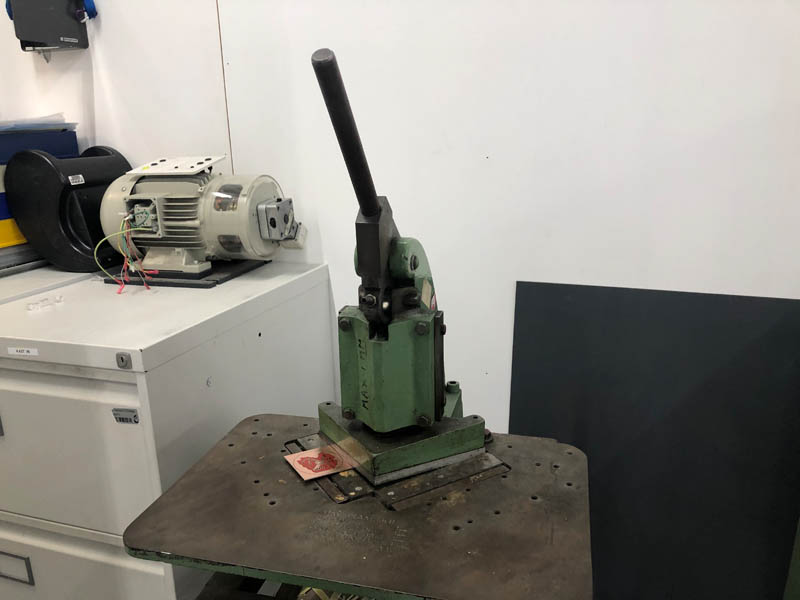
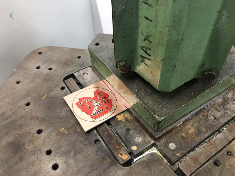
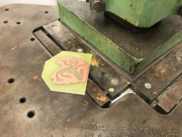
The outlines are not cut in this printing process. Cutting can be done manually with this old school machine. Takes 2 minutes.
Finer details with this one.
Close-up.
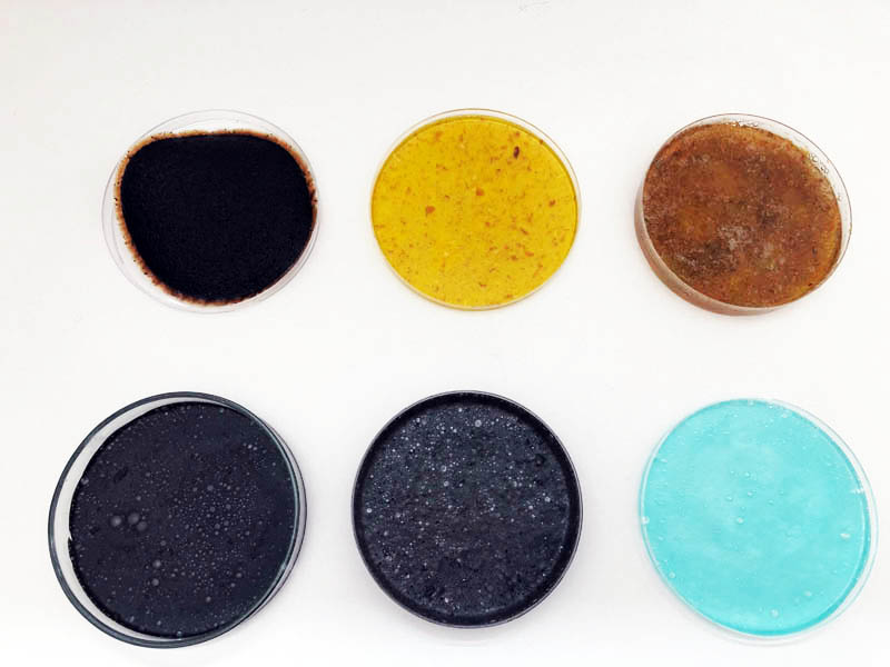
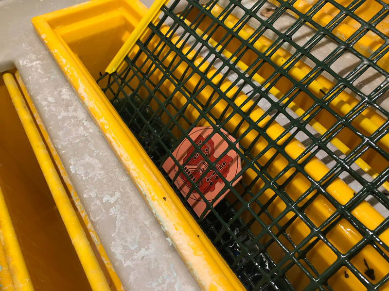
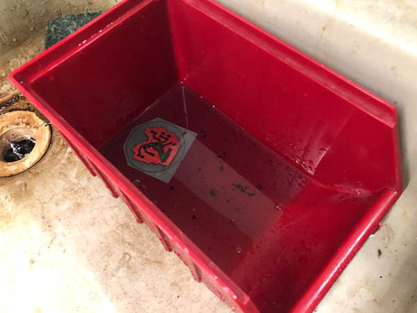
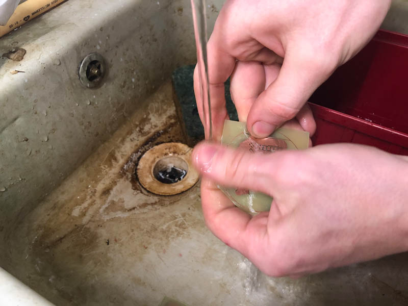
Then we dissolve the copper in a PCB bath.
The material of the PCB bath is Na2S2O8, sodium persulfate. The facility has strict protocols for managing hazardous waste.
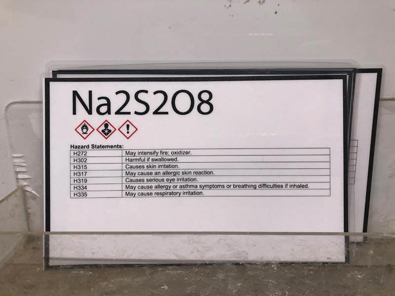
We lower the PCB in this net. Make sure the substance doesn’t touch your clothes.
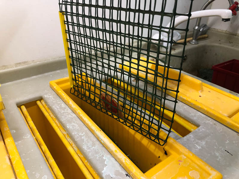
After 10-15 minutes all copper is removed except for the traces. Time: 10:26 AM in bath. 10:34 AM background dissolves, image becomes pink.
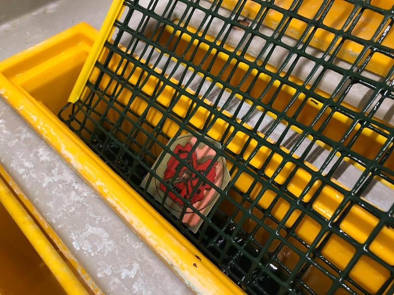
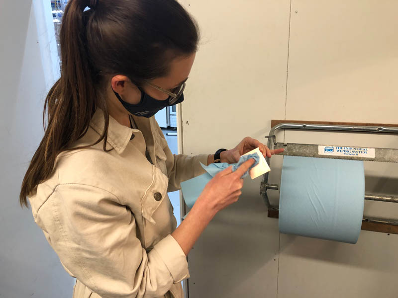
Wash with water.
Dry with paper towel.
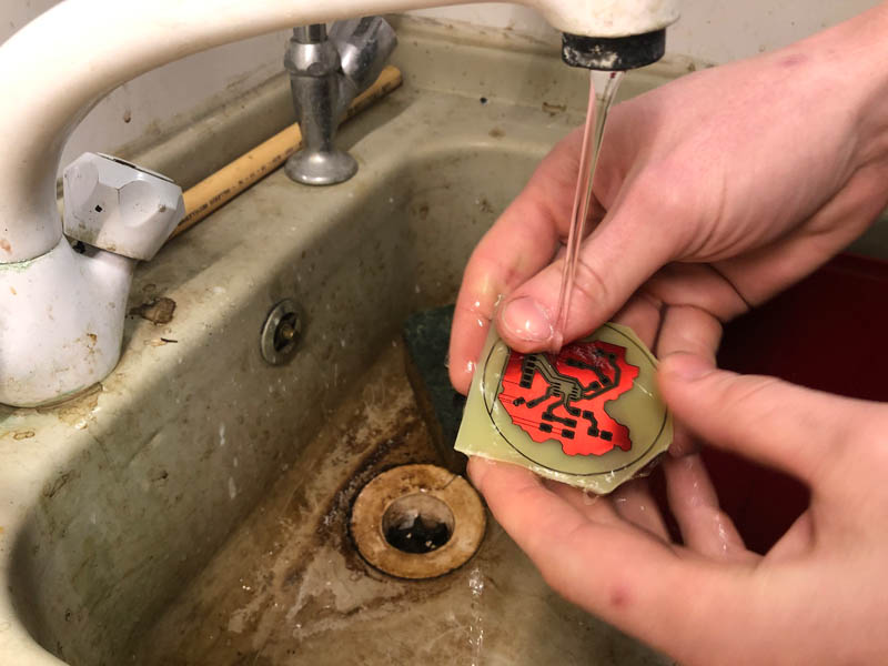
Place in spiritus bath.

Wash off spiritus with water.
Dry again.
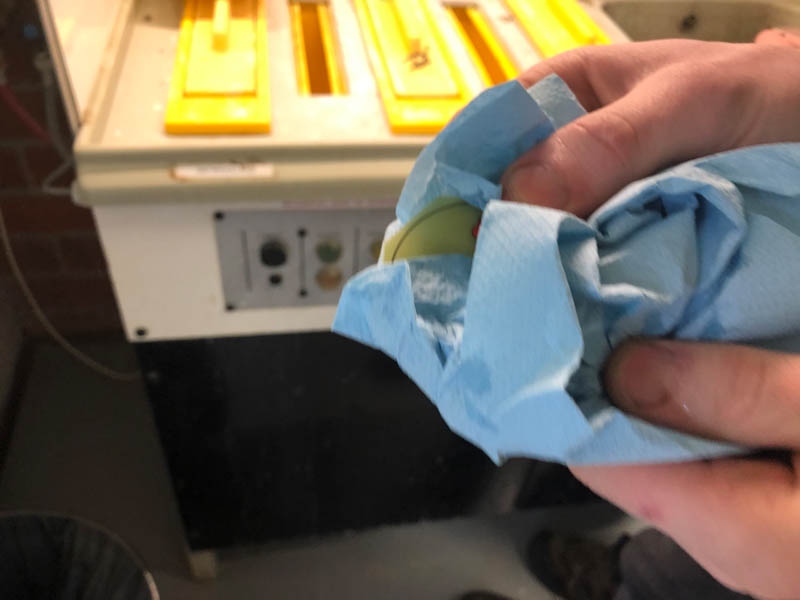
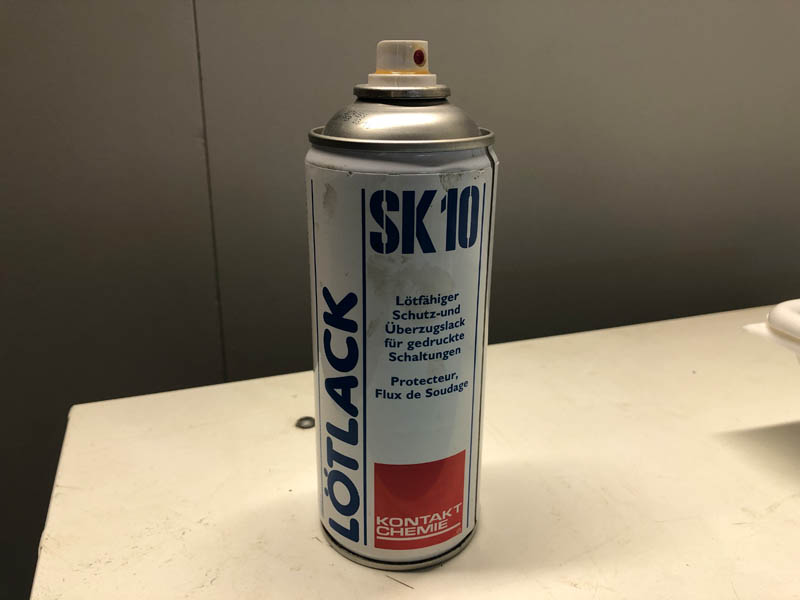
Spray with SK10 solderable lacquer. This provides protection for printed circuit boards or soft-solderable metals against corrosion while making further processing easier. The flux is based on natural resins (DIN 8511 F-SW 31), however contains hazard statements.
Cut the rest of it. Next time, I’ll do all of this in step 8, because the PCB becomes sticky after step 13.
Soldering
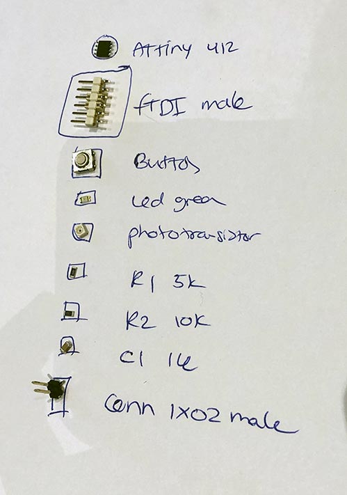
Unfortunately, the Fab Academy electronics kit did not contain all components for this assignment, so I had to travel to Amsterdam for soldering the PCB.
Components collected:
- ATtiny 412 datasheet
- FTDI male
- botton
- Green LED
- Phototransistor datasheet
- R1 4.99k
- R2 10k
- C1 1u
- Connector 01/02 male
Directionality
Next, look up the serial numbers in the Fab Academy components inventory. Then determine if components have directionality. They usually contain polarity marks to indicate in what direction they have to be soldered.
For example:
- ATtiny: the direction of the component is indicated with a dot in one corner. This is the VCC side.
- LED directionality: from anode to cathode. In the LED digikey factsheet we learn that the cathode is green. However, it’s really hard to see! Trying to find guidance with documentation here.
- Button component does have a polarity as well.
- Phototransistor directionality? Rationale: Yes, because on the ATtiny, the polarity mark is on the VCC, I’m going to assume it will be the same with the phototransistor.
Soldering
First, I started with soldering the component in the middle, the ATtiny412.
That went pretty well.
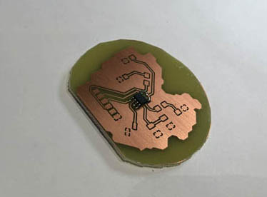
I continued working clockwise, and started with the smallest components first.
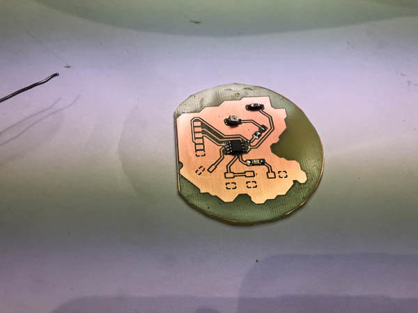
Soldering issues
There was a problem with ‘jumping’ solder, especially when I soldered the GND parts. Solder would hit the copper, and split in little ‘balls’ that would bounce all over the board and table. Also, when this happened, the board was filled with oily flux, creating a repellant layer.
The first reason could be that the distance between the traces might be too small if it’s ground plate. This was told before working with the UV printer. And indeed, the solder only ‘jumped’ from the PCB when I soldered GND. The rest of the touching points on other traces went relatively well.
A second reason could be the applied SK10 spray. That’s wy I removed grease and excess flux with soap and a cotton swab. After that it went better.
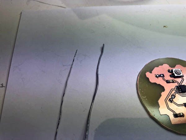
And lastly, I found out that solder of 1.0 mm is way too thick!
When using a smaller wire, soldering went much better.
After a bit of a bumpy road, this is the final result!
Testing the board
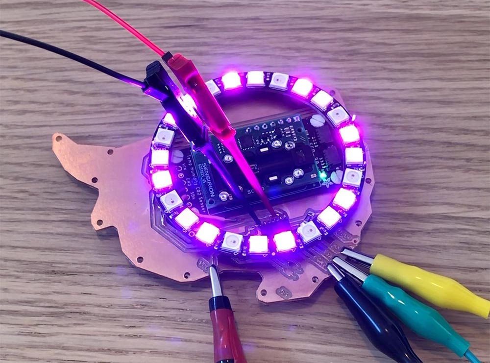
In week 8 about Embedded Programming and week 10 about Input Devices, I learned how to debug this board with a multimeter and logic analyzer. It turned out that the traces of the phototransistor were not connected properly. There also might be an issue with the all-ground plane or material incompatibility of the solder mask applied after the UV printing process. Lastly, it is a possibility that the ATtiny is not working.
Therefore, I redesigned and remade this new board with a regular PCB milling process in week 10. With this board I was able to successfully upload the Hello Echo program, blink an LED, turn a button on and off and program a phototransistor.
It was exciting to learn about an alternative method to make PCBs this week. Unfortunately this board didn’t work and I’m happy about the decision to test and remake it in other weeks. I’ve learned a lot!
Downloads
Explore more like this
Week 17 Invention, Intellectual Property and Business Models
After acing through the technical assignments of Fab Academy, the last two weeks have a lighter load so we can focus on the final project. But this does not mean...
Week 16 Applications and Implications
Propose a final project masterpiece that integrates the range of units covered, answering: