Electronics Design
This week we had to redraw a 'Hello world' board.
We had the choice of using ATtiny45 or ATtiny44 for this assignment, and I used the former as the number of its input/output pins were sufficient for this assignment. Here is an example of a working board using ATtiny44.
.Our group assignment was to observe the operation of a microcontroller circuit board in our lab using test equipment. The results are presented here.
As examples of other people who used KiCad and their board worked I looked at this.
I chose to download and install KiCad to draw the schematic and make the PCB design based on recommendations from our instructors. Though I also have Eagle installed with the same education license as Fusion 360, so I may give that a try later as well.
While I did use Eagle as part of the assignment in week 4 to create the traces and layout of a board, I did not get deep enough in its usage, and as such found it a lot more tedious to use that KiCad. So I'm planning to stick to KiCad for the rest of Fab Academy.
The design
Here is the pin configuration of ATtiny45 that I'll be using for this week:
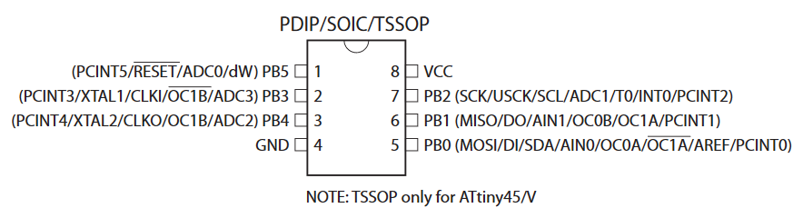
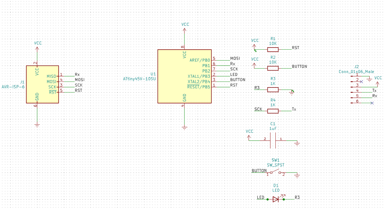
Port B is a 6-bit bi-directional I/O port with internal pull-up resistors (selected for each bit). Sometimes, there's only a certain bit of the port that can be used for a certain puspose, such as serial clock (SCK) or reset (RST), so here's how I ended up dividing the ports for various purposes:
- PB0 (pin 5) -- MOSI (master out, secondary in)
- PB1 (pin 6) -- Rx
- PB2 (pin 7) -- SCK
- PB3 (pin 2) -- Button
- PB4 (pin 3) -- LED
- PB5 (pin 1) -- RST
The two other pins of the microcontroller are connected to VCC (5V, pin 8) and Earth (pin 4).
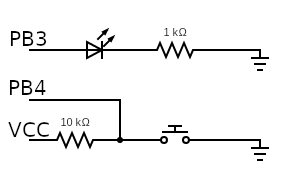
A pull-up resistor is one that connects a component to Vcc and a pull-down resistor is one that connects a component to the ground. This is done in order to avoid the value of a pin from floating, i.e. picking up unknown values effectively making it uncontrolled.
I have to make sure that the values of pin 3 (PB4) which is going to be an input pin and is connected to the button is not floating under any circumstance. For this reason, I decided to use a pull-up resistor to connect it to VCC, so when the button is not connected, the voltage is exactly equal to VCC, and when it is connected, the value at the pin is 0 (grounded). Using a 10 kΩ pull-up resistor effectively limits the current through the resistor to 5 V/10 kΩ=0.5 mA when the button is connected, or in other words VCC is shorted to the ground, which will prevent the resistor from getting hot when the button is pressed.
Pin 2 (PB3) of the ATtiny45 microcontroller will be an output pin used to control the LED. The maximum voltage of the pin will be equal to VCC, which for our microcontroller can be a maximum of 5 V. On the other hand, the LED can handle a maximum of 5 mA current. According to these two values, the current limiting resistor between the LED and ground can be calculated to be 5 V/5 mA = 1000 Ω = 1 kΩ, which I put between the LED and ground. After checking other circuits, and seeing some put the resistor before the LED, I started wondering whether there is a difference, and whether I should put it before. I looked online and came upon this page which explained that it does not matter whether the resistor is before or after the LED, it'll still protect it from burning out. The typical voltage drop of an LED (the 'forward voltage') is 2V.
Here's how the circuits for PB3 and PB4 should look like: (created with circuit-diagram.org)
Designing the board with KiCad
Starting a project
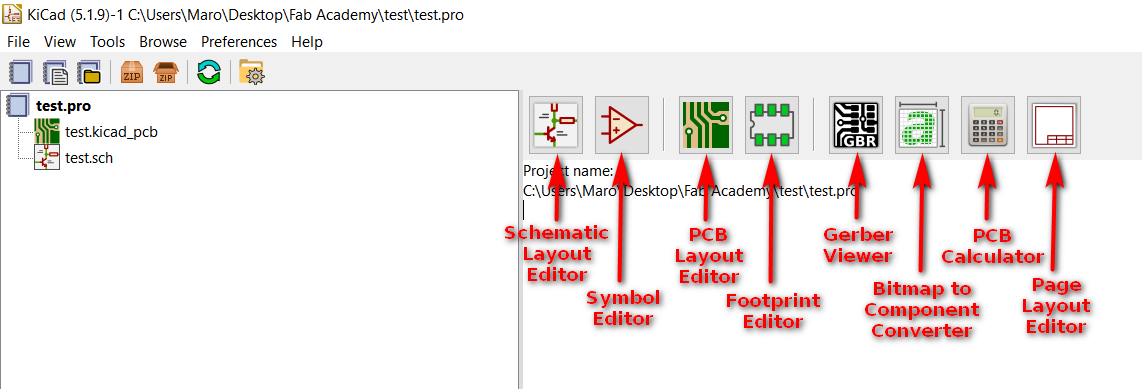
I used this tutorial to get acquainted with starting work with KiCad. To start, new project should be started, which opens up the following screen:
I had to design my Hello World board twice, each time starting from scratch. The reason was that the routing could not be completed for my first board, and my first schematic also happened to be pretty messy due to the wires everywhere. So in my second design, I forgo of the wires in the schematic, and came up with a completely different tracing.
Designing the schematic
The .sch (schematic) file must be opened first. Then new components should be placed by clicking on 'place symbol', and new ones can be selected by typing their name.
Here are some great shortcuts:
- By holding M on the keyboard and hovering over a component, it can be moved.
- Pressing R while hovering over a component rotates it by 90°.
- Pressing C while hovering over a component copies it.
- Pressing E while hovering over a component allows one to change the value (e.g. 5kΩ) and position coordinates of the component.
- For ending the wire while drawing it, press K.
After the components are placed, the 'place wire' shortcut is selected, which allows connections to be placed between the components. This is what I attempted for my first design of the board, and here's what I came up with:
From the mess that my initial schematic became, I learned that it makes sense to label component pins that should be connected instead of neccessarily connecting them with wires. Here is a nice tutorial about how to do that.
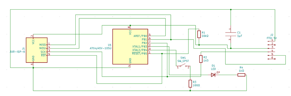
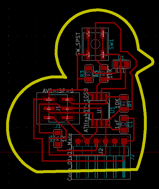
So I came back and designed the schematic again, this time using labels for connections instead of placing graphical wires. The result was a lot less mess, more readability and visibility. Here's my second attempt at the schematic:
Then the components can be annotated, which causes each component to be automatically named and numbered based on how many components there are.
For designing the PCB, 'Generate Netlist' should be selected, after which a .net file is generated. After that click on 'Assign PCB footprints to schematic symbols'. A new window opens which is devided into three columns: the left column shows the categories from which components can be selected from, the middle column shows the components of your schematic, and the right column shows the individual components from the categories selected. After selecting a component type for the schematic component, you can click on 'View component footprint' to check whether it is the intended component. Close the window to get back to selecting components. Once done, select 'Apply, save schematic and continue' and then 'OK'.
Here are the component foorprints chosen for my first attempt at designing the board:
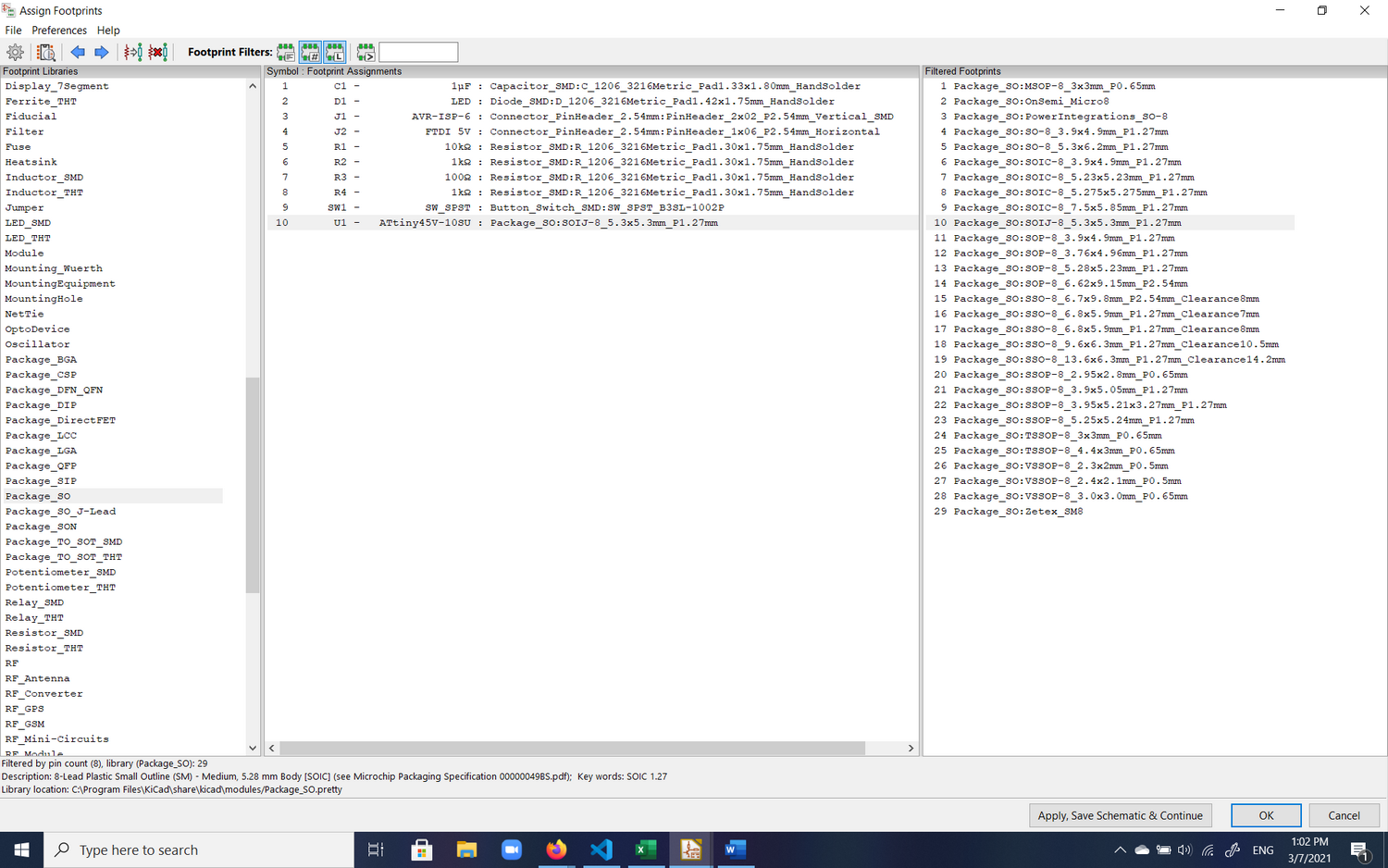
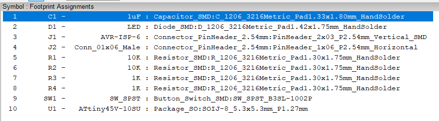
Second time around, these are the footprints I chose:
You then have to 'Generate Netlist' again. The click on 'Run PCBnew to layout printed circuit board' to open the PCB Layout Editor, where you can start creating traces and routing the components.
The PCB layout
Once inside the PCB Layout Editor window, click on 'Load Netlist' and choose the corresponding file. Now you can see the footprints for all the components you chose in the Schematic Editor window. The connections you defined in the schematic are now shown by temporary lines which will disappear and be replaced as you trace each connection.
After importing footprints, tracks should be rearranged so they don't overlap with each other. The shortcuts are the same as before.
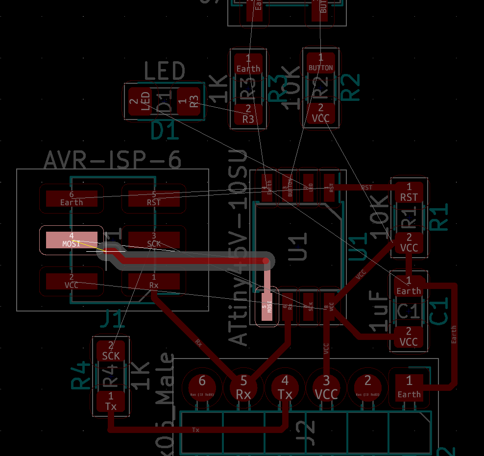
Here's how the components were first rearranged after importing my first design of the board:
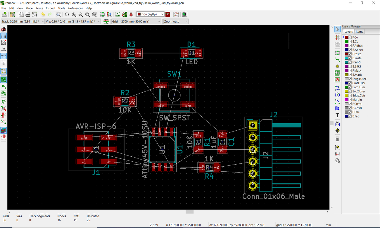
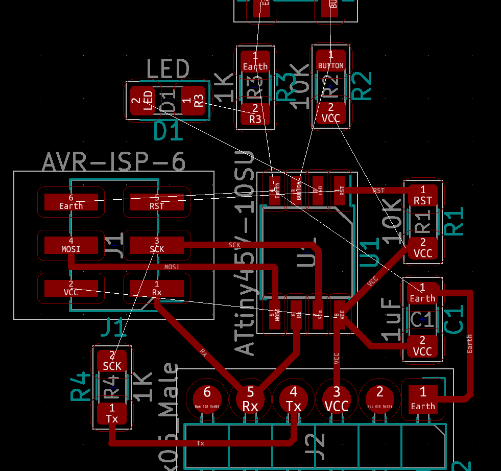
And here's the rearrangement of components a little while later:

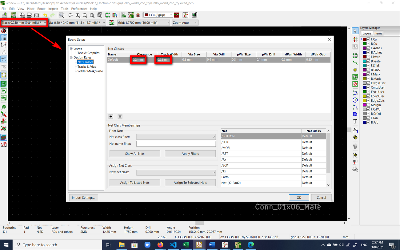
Before routing, design rules should be taken into account. The Design Rules for the entire board can be set from 'Edit Pre-defined sizes...' and then selecting 'Net classes', from which also clearance value can be defined. For individual tracks and vias use 'Tracks and Vias'.
The track size can be adjusted from the drop-down menu at the top-left. You can choose 'Edit predefined sizes' to choose a custom track size of 0.4 mm. You can then select the type of your board, so for example upper copper means the tracks are placed on top of the board, and bottom copper means at the bottom. The select 'Route tracks' and start routing your PCB. You can right click and choose 'Place Through Via' and double-click to build a via through the board.
Here's how tracing is done:
Here's how the tracing progressed on the board:
After finishing the routing, you can select 'Edge.Cuts' to create the exterior cut, and choose 'Add graphic lines'. Also, select 'change cursor shape'. Once done, right click and 'Cancel' to stop.
Here's how the edges on the final design of the board (the chick) ended up:
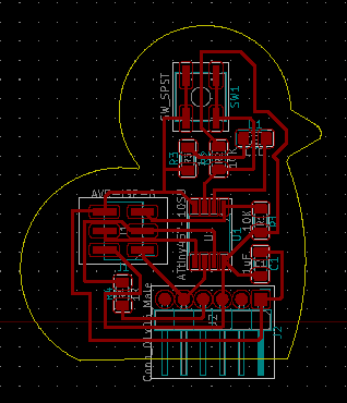
The edges are pretty thin, so that could be adjusted through the design rules. Here's what the final traced design looks like:
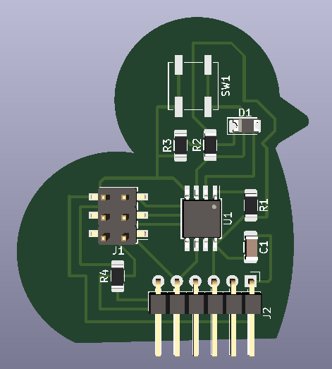
Then you can go to View -> 3D Viewer. In my case, this is what the 3D visualization of the board looked like:
If you need to create mounting holes, click on 'Add footprints'. Then click on an empty spot and choose 'Mounting holes', e.g. M3. Again, change the names you want printed on the board by pressing E on the keyboard.
F.Fab and B.Fab layers can be unselected since they won't be printed. The names that will be printed are the ones in blue, shown in the F.SilkS layer. 'F' stands for 'Front' and 'B' stands for 'Back'. To add custom text, click on 'Add text to copper layers or graphic text', choose F.SilkS and write the name of the board or any other text.
At the end, you may add fill zones by clicking on 'Add fill zones' by choosing the outer edge and going over it once more. The files can be exported as gerber files. After clicking on 'Plot' click on 'Generate Drill Files...' and then click on 'Generate Drill File' and 'Close'.
At last, the KiCad design was complete. The design could be exported as .svg (scalable vector graphics) to be used in the next step.
Adjusting the graphics of trace and outline files
Once KiCad has output the trace and outline files, they can be adjusted for milling using a graphics editor such as Inskape, which is a free graphics software I used. This is especially important since the outline is output as an edge by KiCad, which would require two cuts on two sides of it, but we really need one cut to be made for the board to come out, so just differentiating the inner and outer parts of the outline using Inskape is enough.
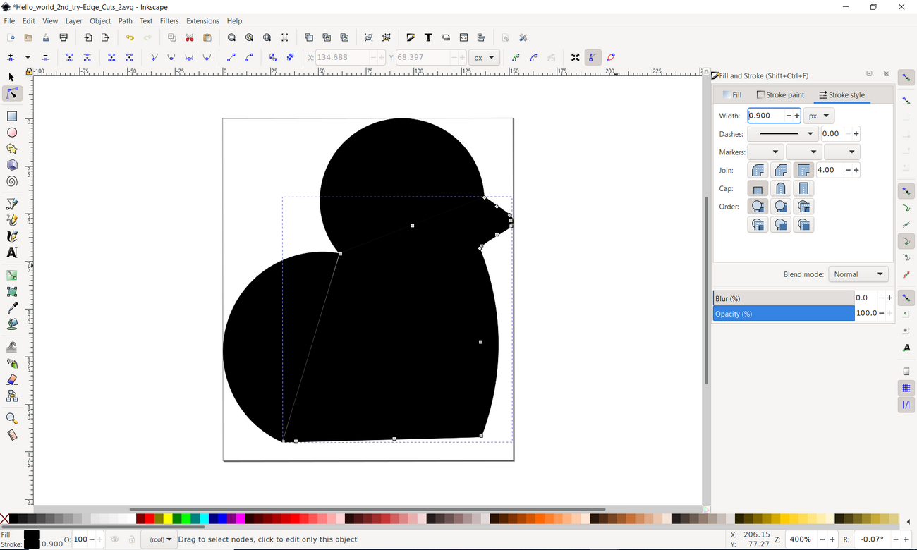
Another important point to keep in mind is for milling to work right, the trace and outline files should of the same size and able to be juxtaposed, so while saving it in Inkscape that is another factor to consider.
Preparing the G-code
G-code or NC-code (numerical control code) is the code needed for a CNC machine (a Roland SRM-20 milling machine in this case) to be able to mill the product.
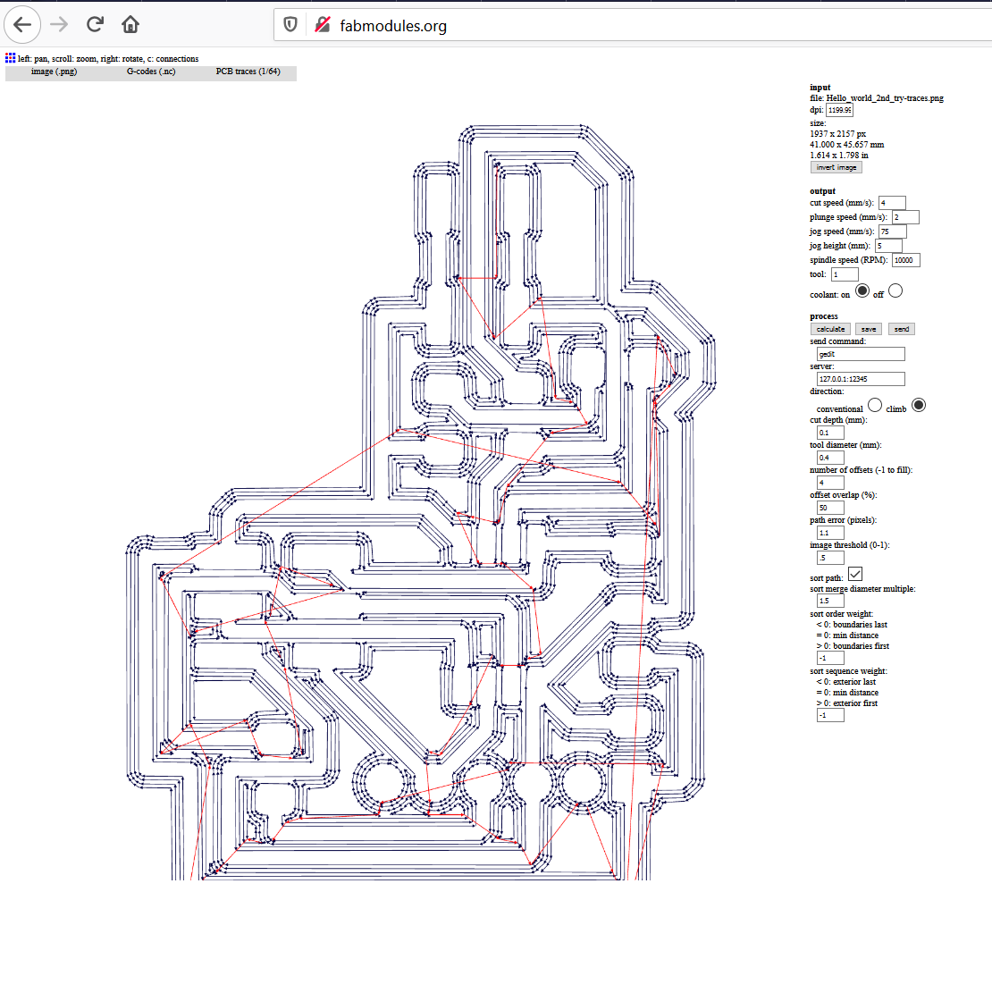
Once the .svg or .png files for the traces and outline are ready, the G-code containing the milling paths for the board can be generated using fabmodules.org, a website written by Neil Gershenfeld and others. It has later been replaced by mods.cba.mit.edu, but for this course it sufficed for me to use the older simpler version.
Once the .svg file is uploaded into fabmodules.org, the output format can be chosen as .nc (G-code), and then the process of milling identified as either PCB traces (1/64") which is used to mill traces of the board, or PCB traces (1/32"), which is used for milling the outline of the board. Once the process has been selected, number of offsets can be adjusted. This shows how many times the milling bit will go over the generated path; 4 is a reasonable number of times resulting is smoother edges along the paths. Another important option is the 'invert image' option which switches the black and white regions of the file.
Here's the toolpath of the traces of the board generated for my Hello World board using fabmodules.org:
Milling the board
Milling of the board was done using a Roland SRM-20 CNC milling machine available at Fab Lab Dilijan.
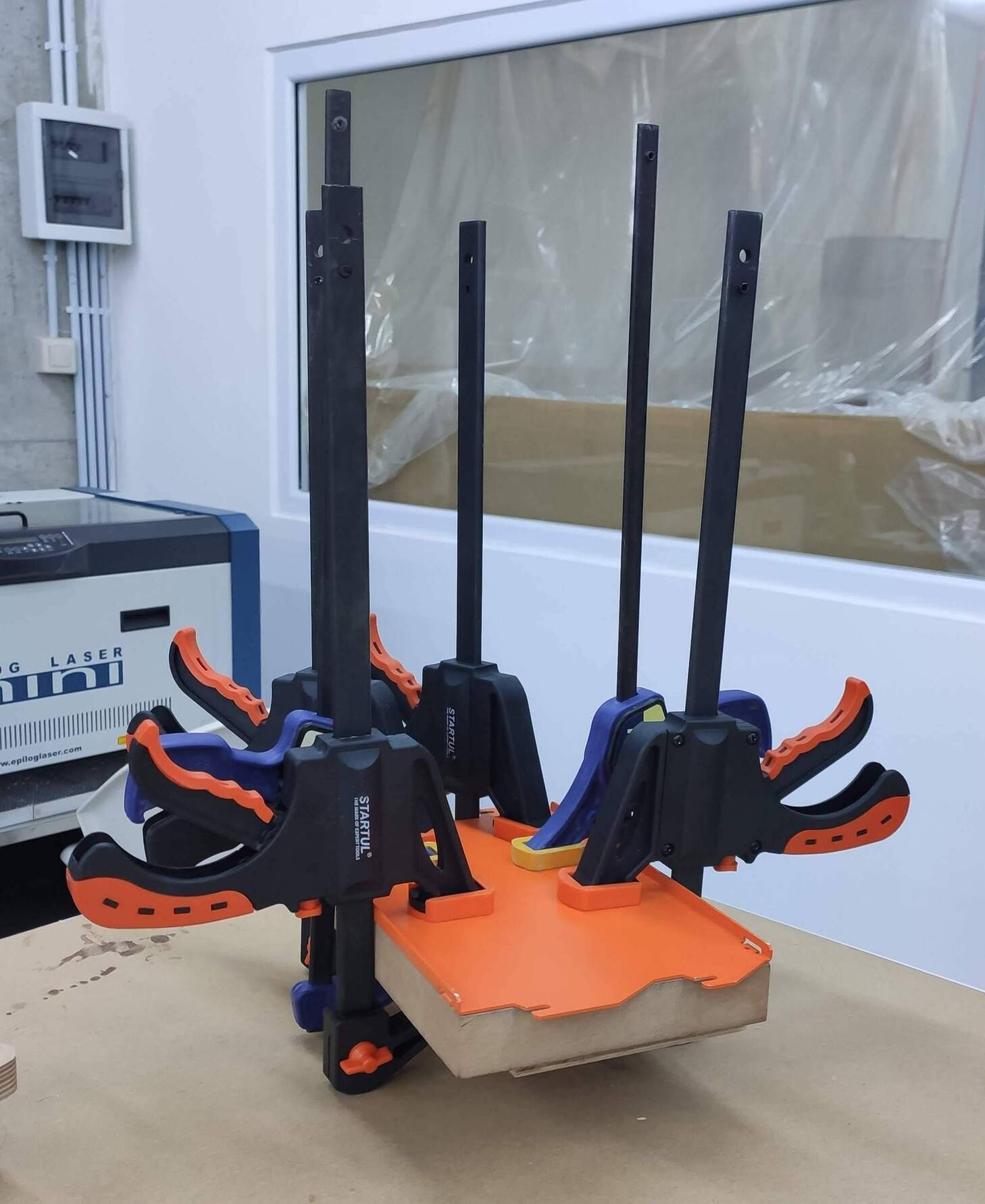
Before milling the board, an FR-1 PCB Blank had to be attached using a 2-sided tape to the platform of the Roland SRM-20. In order for it to be straightened out in case of any warps or bends, it had to be clamped down and left so for about half an hour, after which the clamps were removed and the platform was attached back inside the Roland SRM:
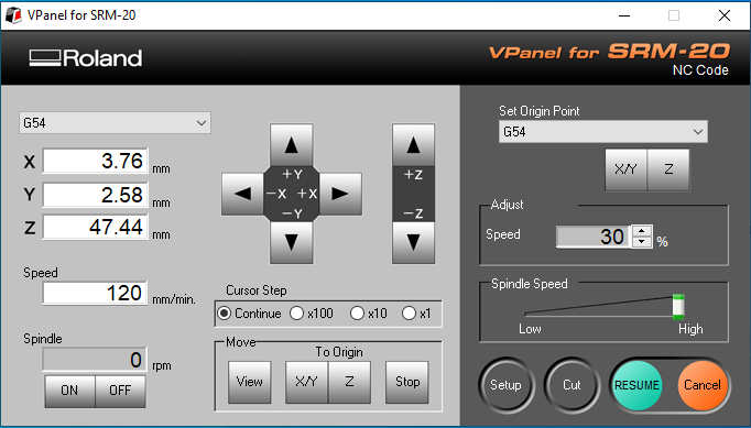
The relevant G-code can be selected from V-panel for SRM-20, which is the software controlling the machine, and the translational and spindle speeds can also be adjusted during the mill.
Here is the interface of the V-panel software controlling Roland SRM:
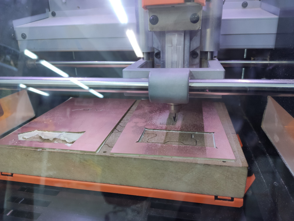
And here's the machine milling the board:
Here is the milling result for my first board (the penguin), which I didn't like due to the complication of the traces and had to redesign:
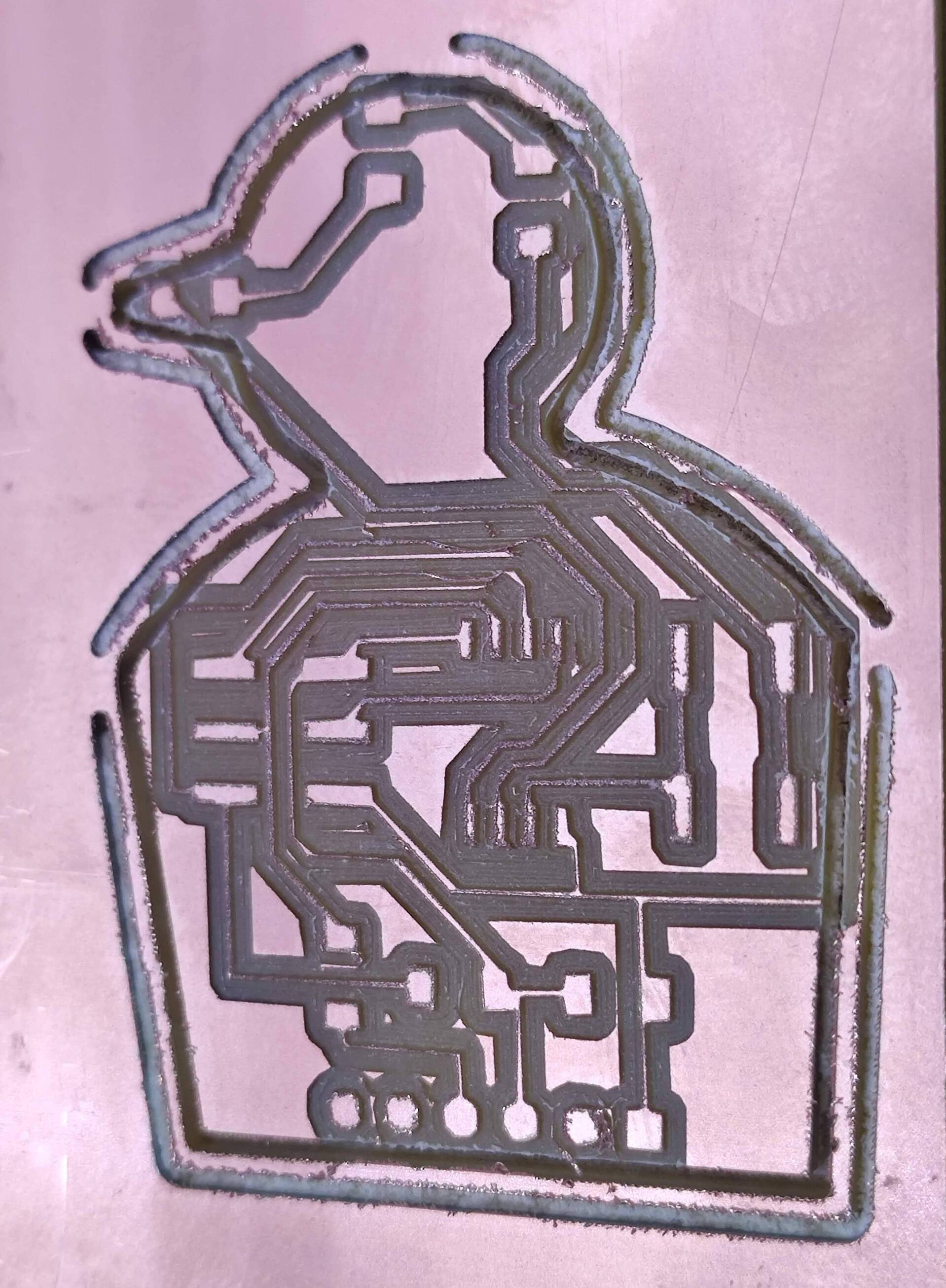
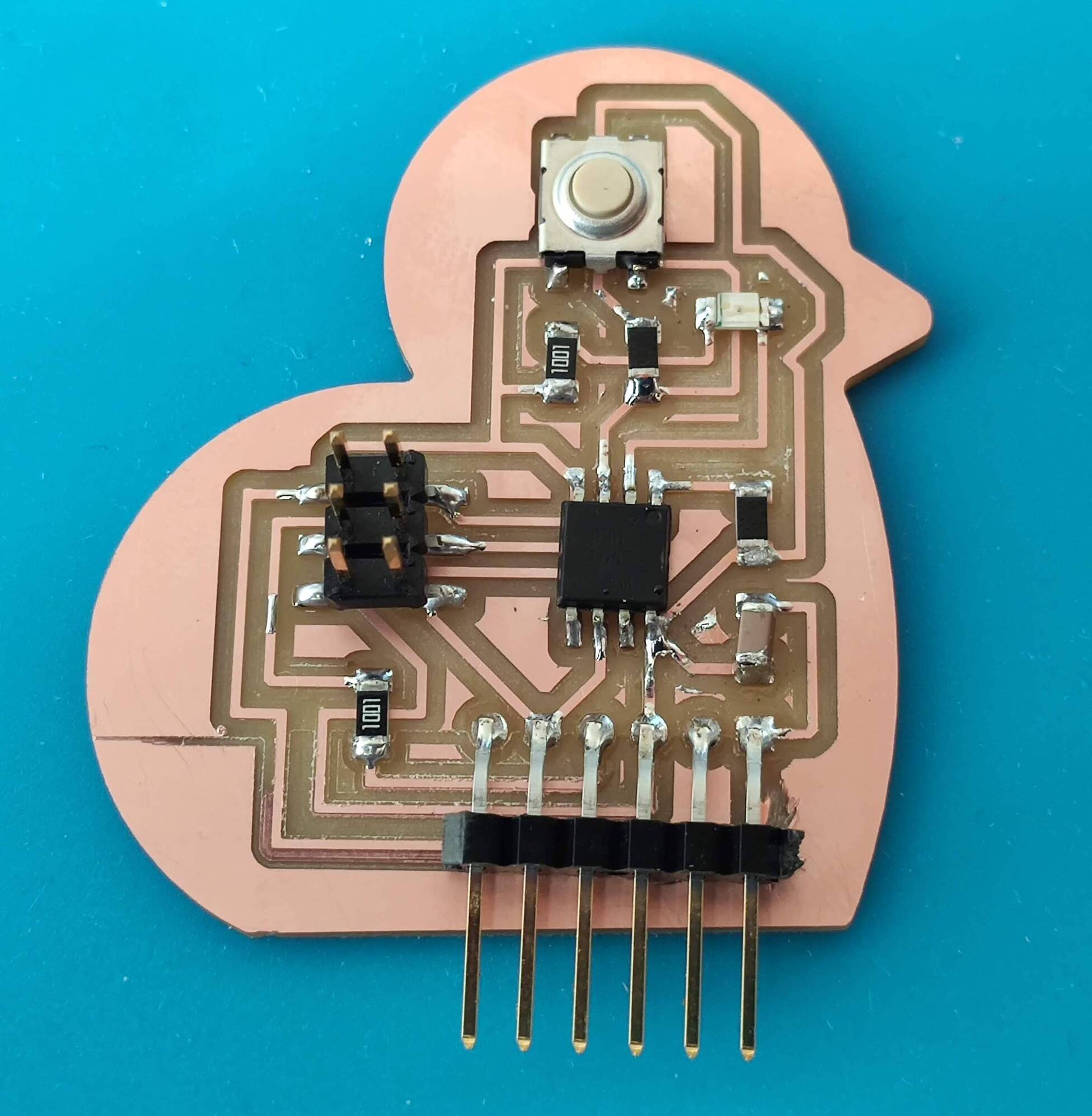
And here's the result of milling my second board (the chick):
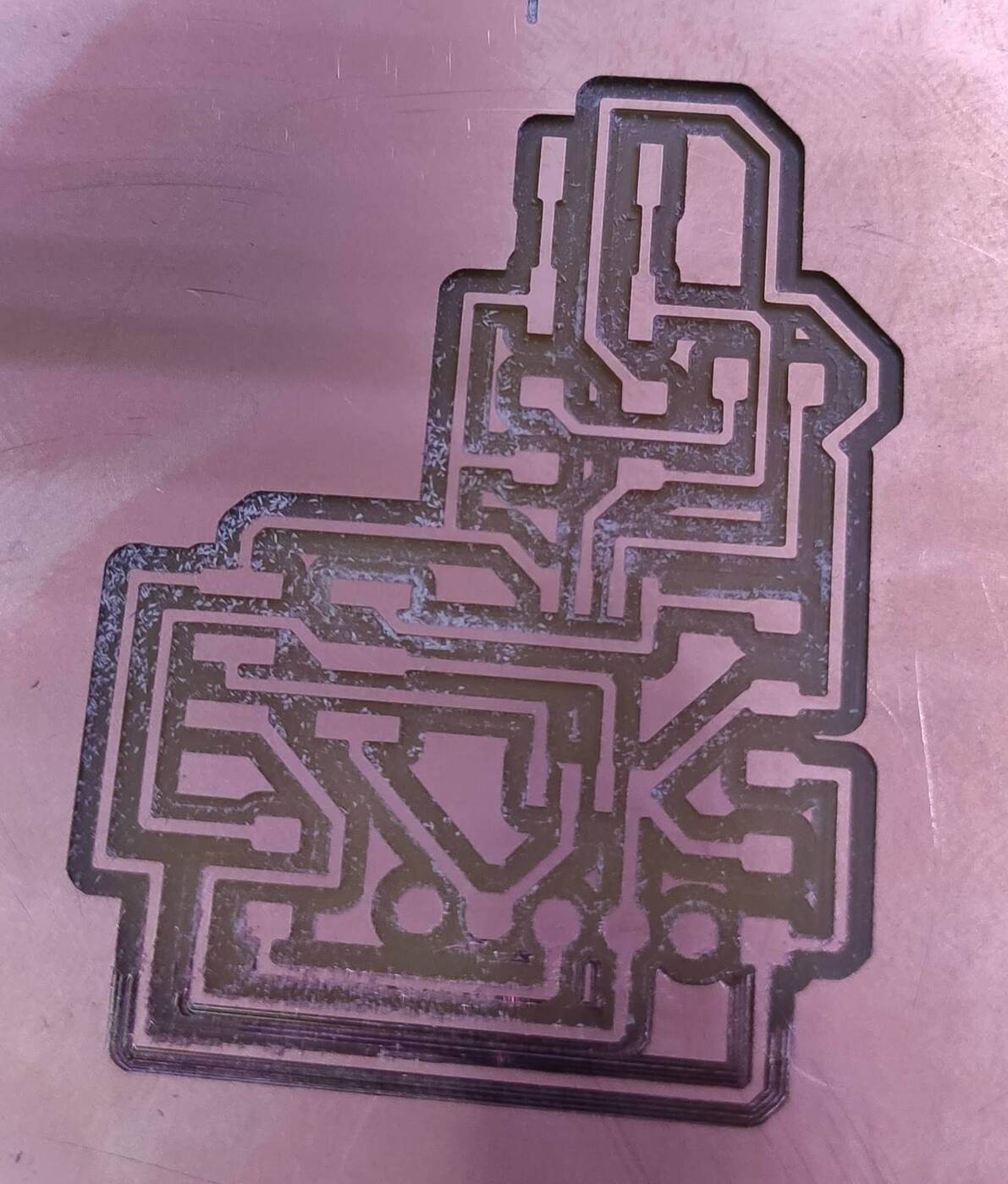
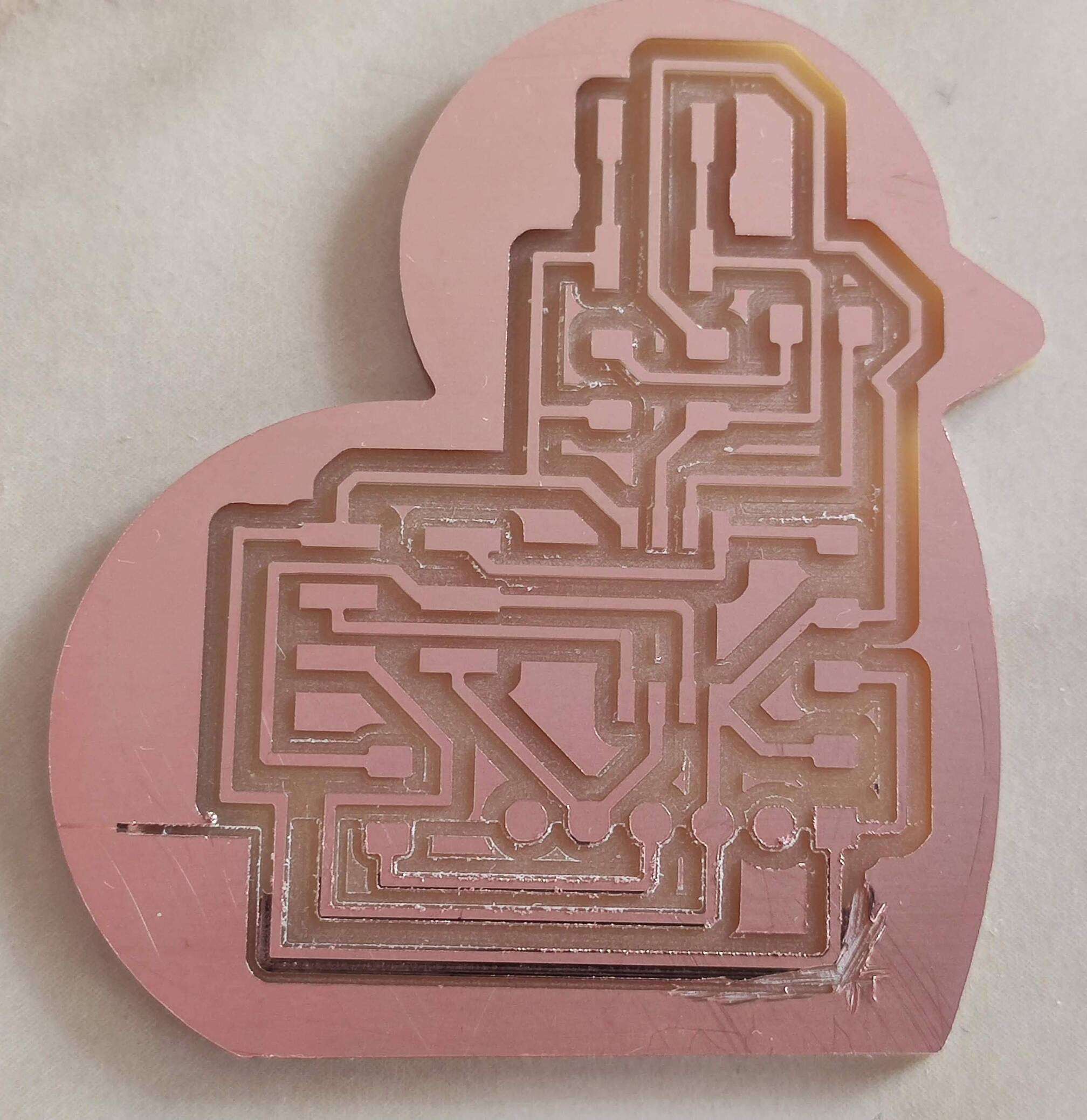
As can be noticed, the bottom part of the chick was not milled quite right. This was due to the fact that the PCB board was actually slightly warped, so the mill bit would go over the bottom part, but only polish it and not be able to mill a track. In order to fix it, I adjusted my file in Inkscape to only leave the bottom part to be milled over again. However, since the top part was cut off, the G-code generated based on the file treated the top of the image as an edge, and therefore at the end the milling bit went out of the bounds a bit (to the left), which was manually stopped. The right side was also manually adjusted later, as the milling bit still had not been able to mill the tracks there and only polished the copper.
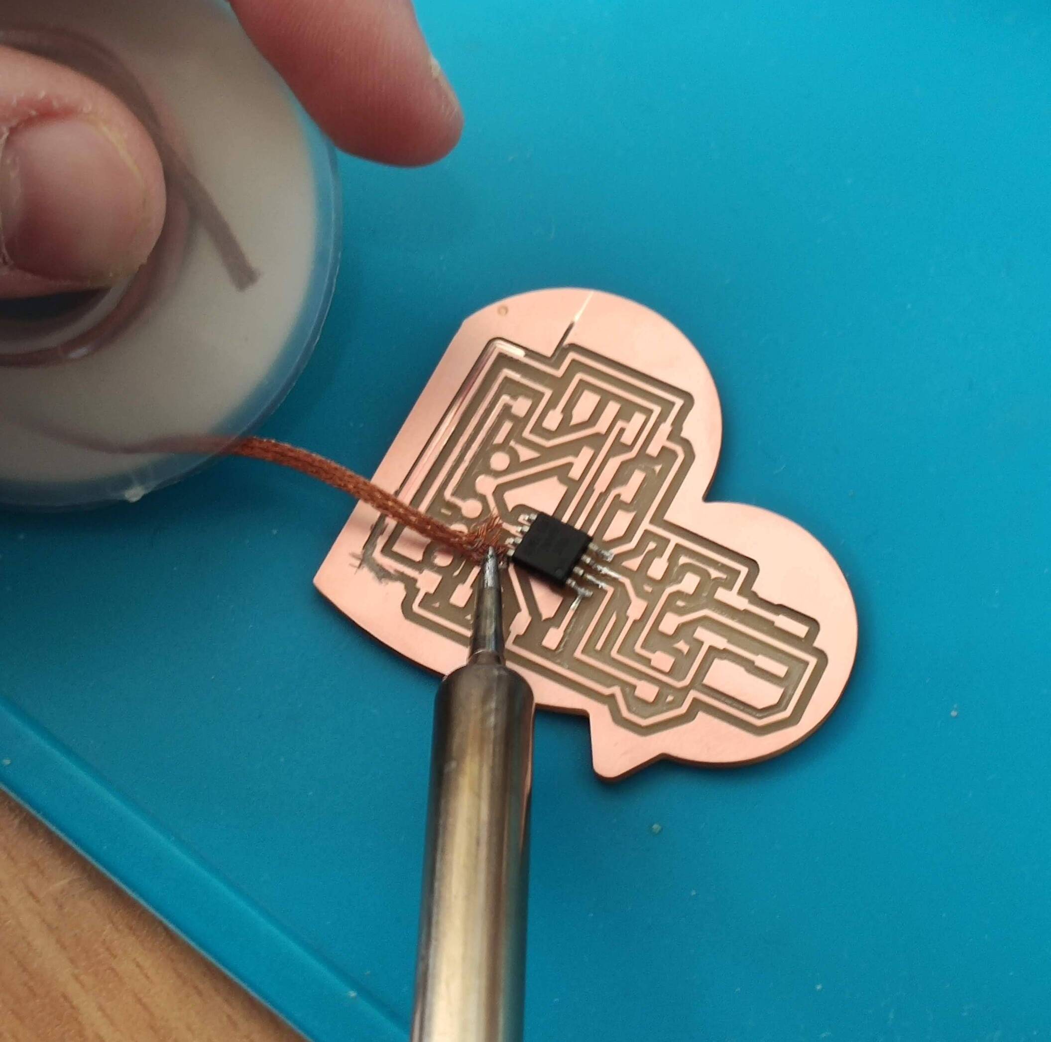
Soldering the components
The components for the board were then soldered on according to the design, starting with the ATTiny45 microcontroller. If I had too much lead on one pin, I could wick it off as so:
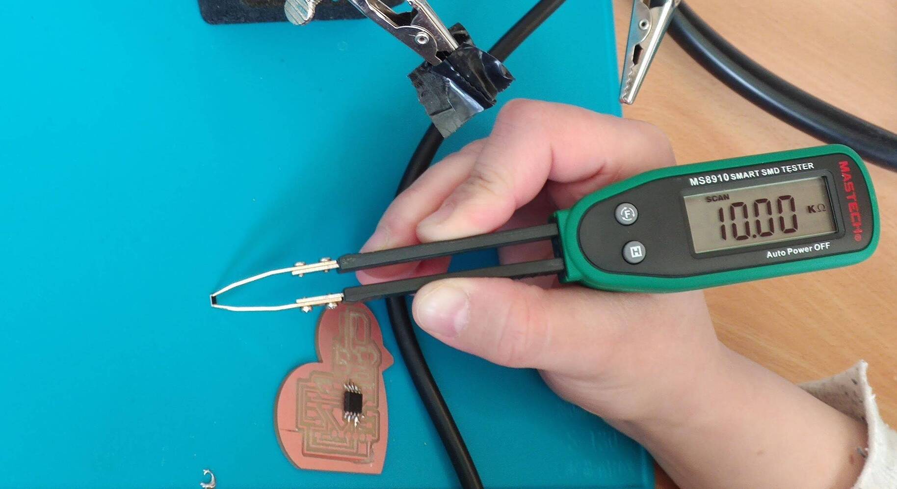
A great tool that I used this week was my husband's SMD smart tester, which allows one to measure the capacitance or resistance of a component by just picking it up with the tips of the tweezer test; a pleasure to use:
Here's what the final result looked like:
FAQ about the circuit
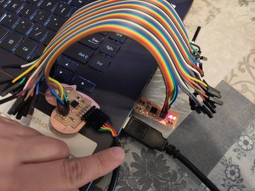
Programming the chick
Since I use Windows, I had to follow this tutorial by Brian to be able to use the GNU AVR toolchain on Windows 10. I used FabTinyISP to program the chick, which meant I followed the tutorial till the end. For that, I had to install a generic USB installer called Zadig (which by the way means Easter in Armenian with a Western Armenian pronunciation :) ). Afterwards, I was ready to start programming. Here I found out that the little arrow on the FTDI cable should be connected to the ground.
I lost a whole day because first, I specified the wrong path, and then I did not restart bash and didn't realize that paths don't get updated until restarting it. Very important!!!!!
Then make wasn't working and giving me this error: make: *** No targets specified and no makefile found. Stop.
I changed the name of the file to Makefile and removed all extension, and then it worked.
In any case, the programming was to be completed in the Embedded Programming week, which means the complete story of how it was done can be read there.
Downloading the files
The files for the 'hello world' board with a switch and LED designed with ATTiny45 can be downloaded from the following links:
- The entire project archived in KiCad (.zip, 13 kB)
- The schematic of the board (KiCad schematic file with .sch extension, 8.45 kB)
- The board design (KiCad board file with .kicad_pcb, 44 kB)
- Monochromatic image of the traces of the board (.png, 50 kB)
- Monochromatic image of the outline of the board -- should be inverted for milling (.png, 55 kB)


