Electronics Production
The group assignment for this week was to characterize the design rules for our PCB production process: the feeds, speeds, plunge rate, depth of cut (traces and outline) and tooling. The results can be read here.
This week Dilijan got dealt a generous load of snow. The roads were hardly accessible, but not for the unwavering souls who call Fab Lab Dilijan their Alma Lab. Hence, we had a warm weekend at Fab Lab Dilijan trying to make our PCB's work.

And just as a reminder that the best things in life are free, here's a scene from the weekend in Dilijan: a spontaneously-organized community affair to entertain the neighborhood children on a snow day, because, hey, life demands fun, even after an imposed war in the middle of a pandemic. Especially after that.

And just so my musings don't turn into snoozings, let's divert our attention to...
FabTinyISP
The assignment for week 4 was to make (not design) an already existing in-system programmer (ISP), in this case, a FabTinyISP.
Our instructor Babken recommended that we read Demystifying FabISP to have a better understanding of what the components are for. The page itself has a list of pre-requisites that are also useful.
Producing the ISP could be accomplished in multiple ways, including, but not limited to:
- Using a milling machine to mill the copper off of a copper-coated board,
- Printing the board on a transfer paper, transferring the print to a board with heat, and then etching the board,
- Cutting the circuit from a copper adhesive tape and transfering that onto a substrate.
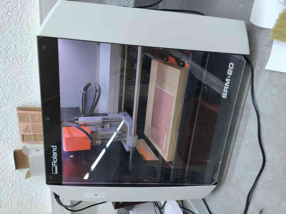
I chose the first method. Fab Lab Dilijan houses a Roland SRM-20, as can be seen below:
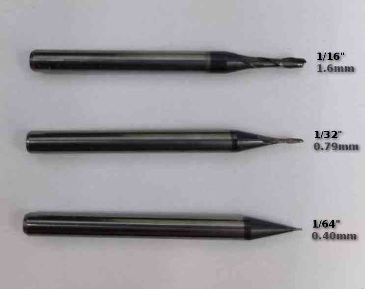
For engraving a PCB, we were recommended to use a 1/64" milling bit, and for cutting out the outline, it was recommended that a 1/32" milling bit be used. A milling bit is different from a standard bit in that its sharp edges extend all the way and the corners form a square on the foremost plane of the bit. The milling bit is capable of making planar cuts perpendicular to its axis as well, as opposed to axial cuts by a standard bit. The following image shows a comparison of the sizes of some milling bits:
Also, in milling a board, the motion of a milling bit can be divided into two kinds based on whether the tangent of the rotational motion of the bit is parallel to its translational motion when it touched the board, or perpendicular. So we get two different milling methods based on that: conventional milling, and climb milling.
- Conventional milling: This is when the tangent of the rotational motion of the bit is parallel to its translational motion when the bit touches the board. In other words, the mill bit touches at the etched part of the board and removed the material by moving to its edge. In this method, more heat is dissipated into the workpiece producing work hardening. Tool rubs more at the beginning of the cut causing faster tool wear and decreases tool life. The chips are carried upward by the tooth and fall in front of cutter creating a marred finish and re-cutting of chip. Also, upwards forces created in horizontal milling tend to lift the workpiece.
- Climb milling: This is when the tangent of the rotational motion of the bit is perpendicular to its translational motion when the bit touches the board. The heat generated from this is then generally dissipated in the cut chip. Climb milling creates cleaner shear plane which causes the tool to rub less and increases tool life. The forced created are hence downward, which help hold the workpiece down.
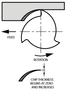
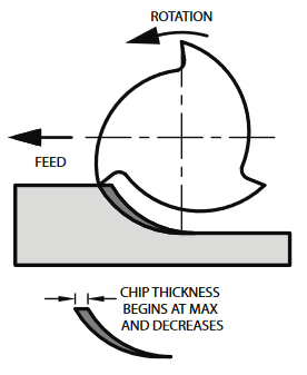 Source
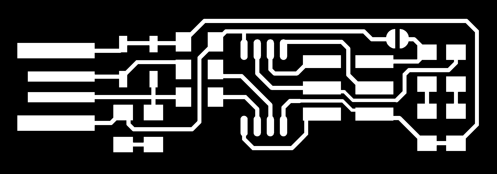
The traces of the FabTinyISP to be engraved were as follows. The image has been made into a .png where the white sections indicate the copper and the black indicates the rest of the board.
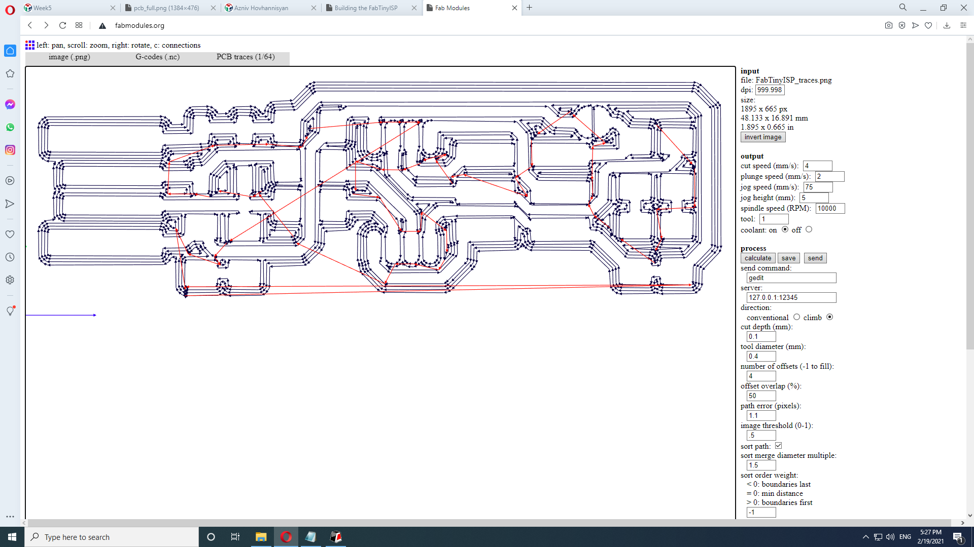
The Fab Modules software was used to turn the png image to G-code, with a .nc extension. The Modules software also shows the path of the milling bit that will be followed in order to create the PCB.
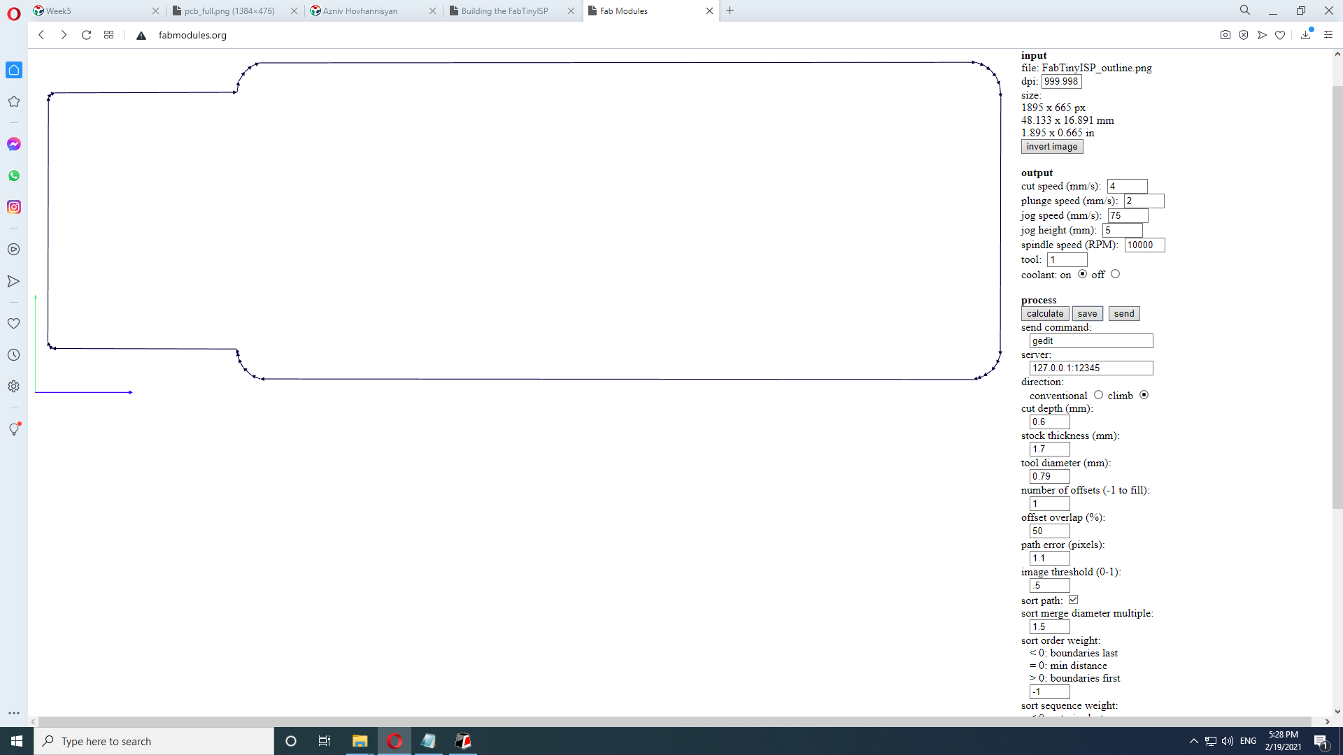
Once the traces of the board are created, the PCB itself has to be separated from the substrate board, which means the outline of it has to be cut out with a larger milling bit, 1/32" in our case. Here white indicates the area of the PCB and black indicates the outer parts.

Once again, the outline png is converted to G-code using the Fab Modules software:
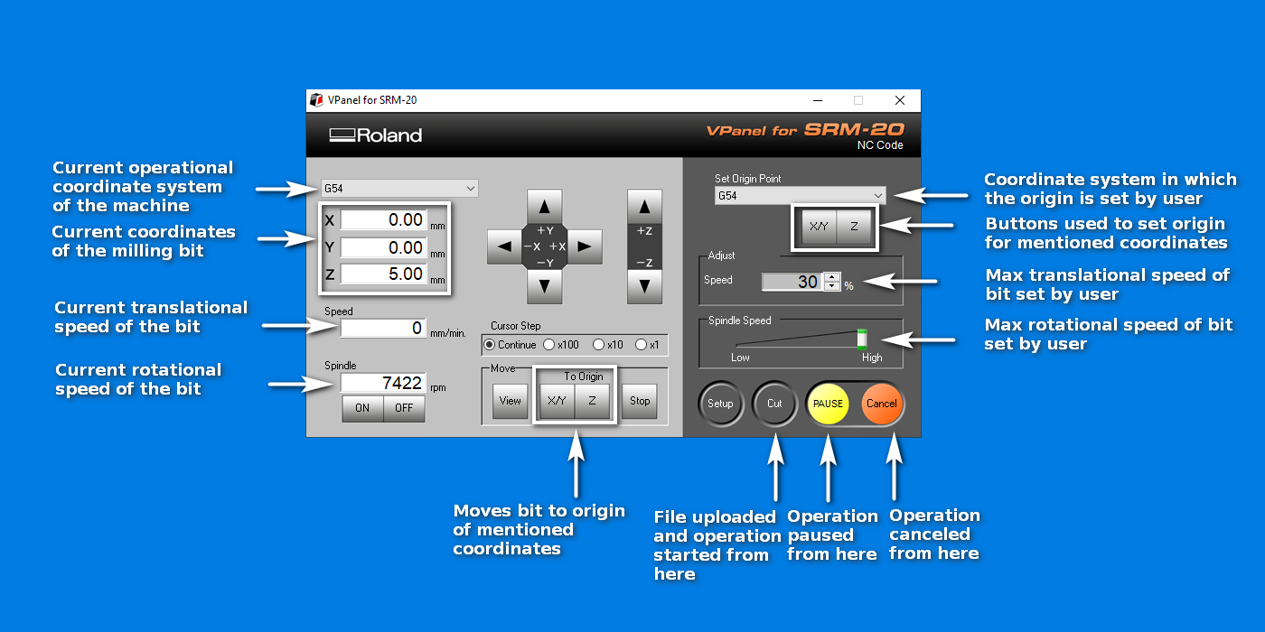
Here is an overview of the SRM-20 software interface, and what each section indicates and controls:
The board to be cut had to be fixed onto the sacrificial material, a wooden block glued onto a metal tray in this case, which had recently been completely flattened using a bit by the lab instructors. A two-sided tape was used to stick the board to the sacrificial block, then another wooden block was placed on top of the board, and two clamps were used to tighten the blocks together and the board was left for 20-30 minutes to get rid of any warps and make sure the board sticks well and flat.
Again, before cutting, the correct milling bit has to be placed in the collet and adjusted. This was the part of the assignment this week that was most prone to accidents, namely, dropping the milling bit on its tip that could break the tip, and could hurt the budget of the lab. In order to avoid that, while inserting or removing the bit with the hex in one hand, the other hand should be used to gently guide the bit by one finger. The same goes for placing the bit on the board to set the z-axis to zero: It should be gently lowered to the surface with a guiding finger. The screw on the collet should be tightened with the long end of the hex to avoid too much torque and dethreading of the screw hole that will make changing the bit very hard if not impossible. Once the z-axis zero is set, the z-axis should be immediately raised using the software control buttons.
The x and y axis zero is set to correspond to the lower left corner of the image that will be printed. It was recommended that the initial translational speed of the bit be set at about 30%, and once it was ensured that there were no problems, then gently raise that during cutting, preferrably when the bit was in the air.
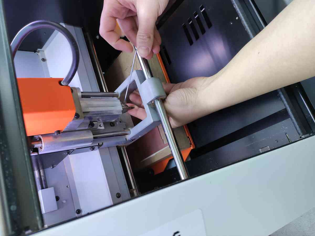
Here the SRM-20 is engraving the board from the front and the side. Considering what material the board is made of, inhaling the dust generated from cutting can present different levels of danger. All materials from FR-1 to FR-4 consist of a thin layer of copper over a non-conductive substrate, with FR standing for Flame Retardant, so the boards can extinguish themselves if set on fire. The substrates are as follows:
- FR-1:Hard paper impregnated with phenolic resin binder,
- FR-2:Hard paper impregnated with phenolic resin binder,
- FR-3:Hard paper with epoxy resin binder,
- FR-4:Woven fiberglass cloth with epoxy resin binder.
Phenolic resin is known for emitting small amounts of formaldehyde and phenol. And glass dust from milling of FR-4 is most dangerous of the four for breathing. So as long as one doesn't blow on the dust, and is careful to avoid ingesting it, one should be fine. More about the different materials and their differences can be read here and here.
The boards at the lab are from Bantam Tools and are made of FR-1, which makes their dust safer than FR-4, the dust of which can have fiberglass and be especially dangerous to ingest.
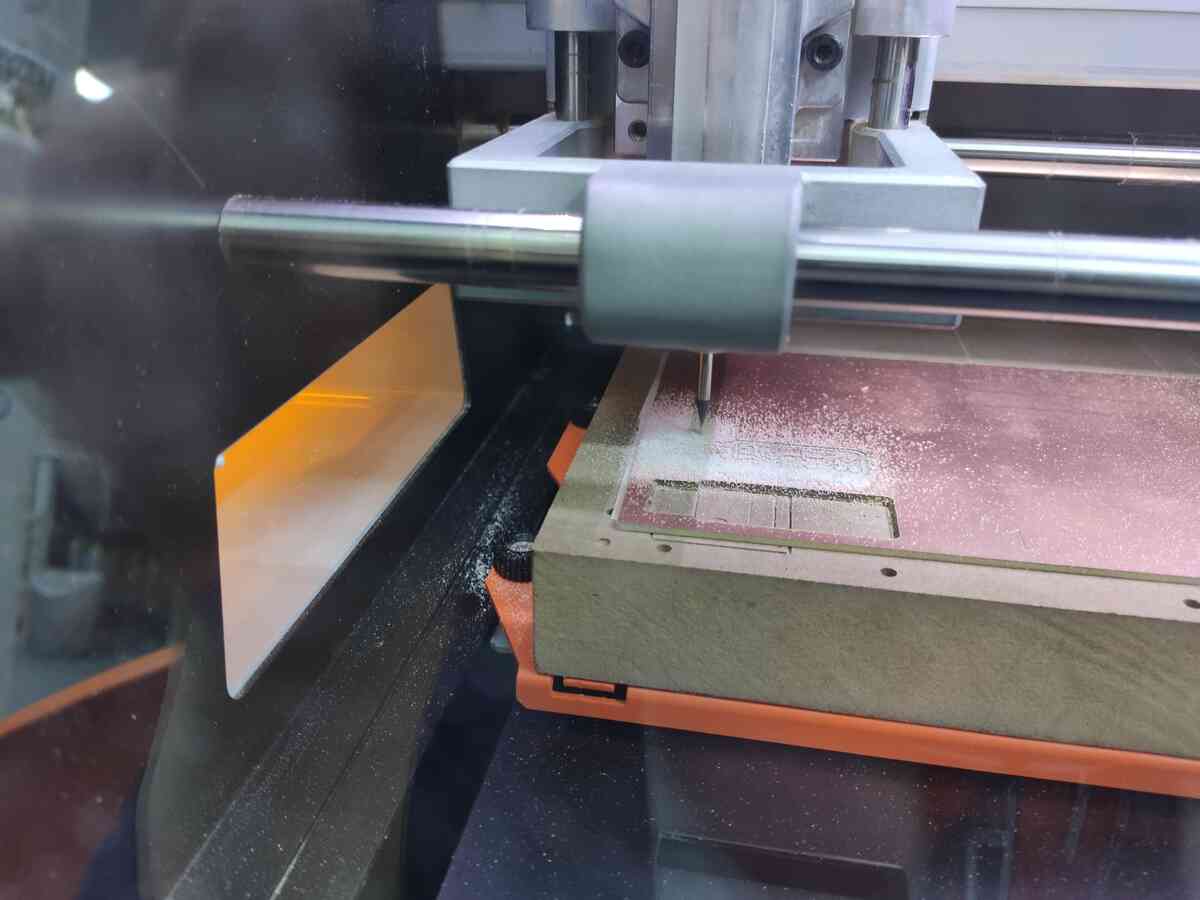
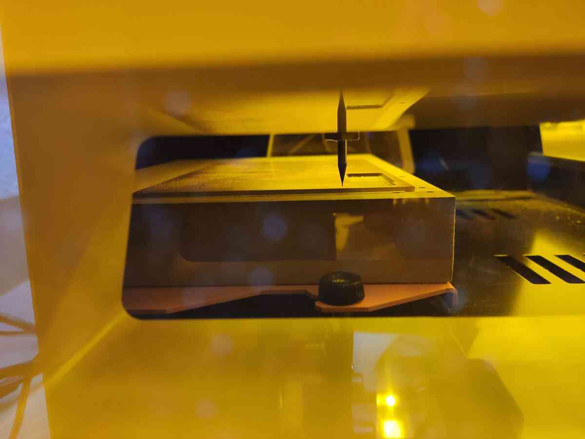
In Fab Lab Dilijan, there is a designated hand vaccuum cleaner for the SRM-20 machine to clean off the dust so that it is not inhaled by brushing it off or blowing on it.
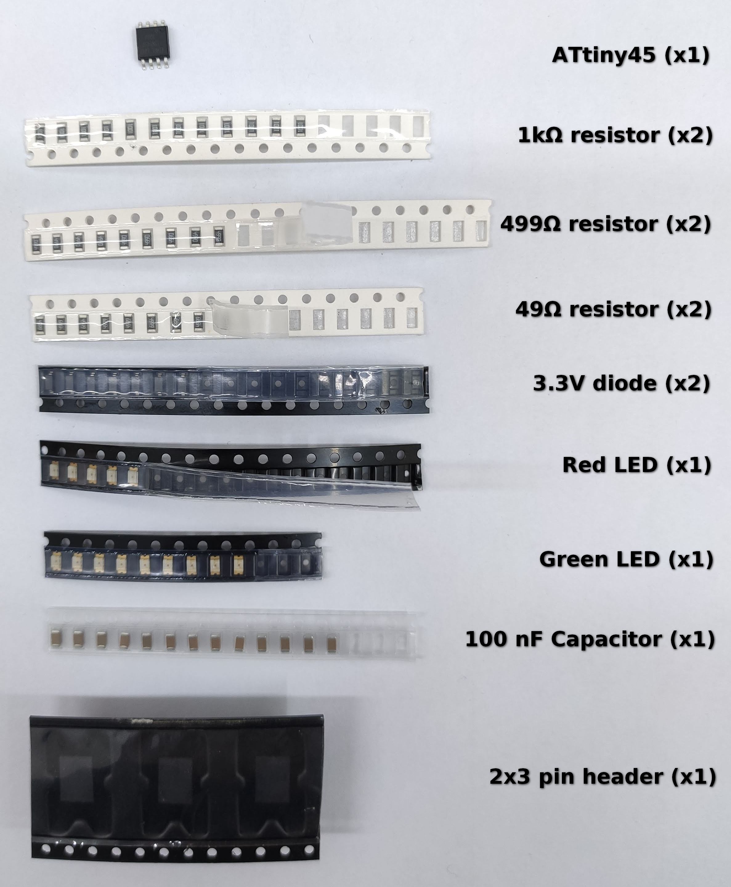
After the circuit traces were engraved and the outline cut out, it was time for soldering on the components. The board was washed with dish detergent and water to get rid of any fingerprint and other debris that would make the solder not stick. Here is a view of the surface-mount devices (SMD's) in their packaging that would be used for the FabTinyISP:
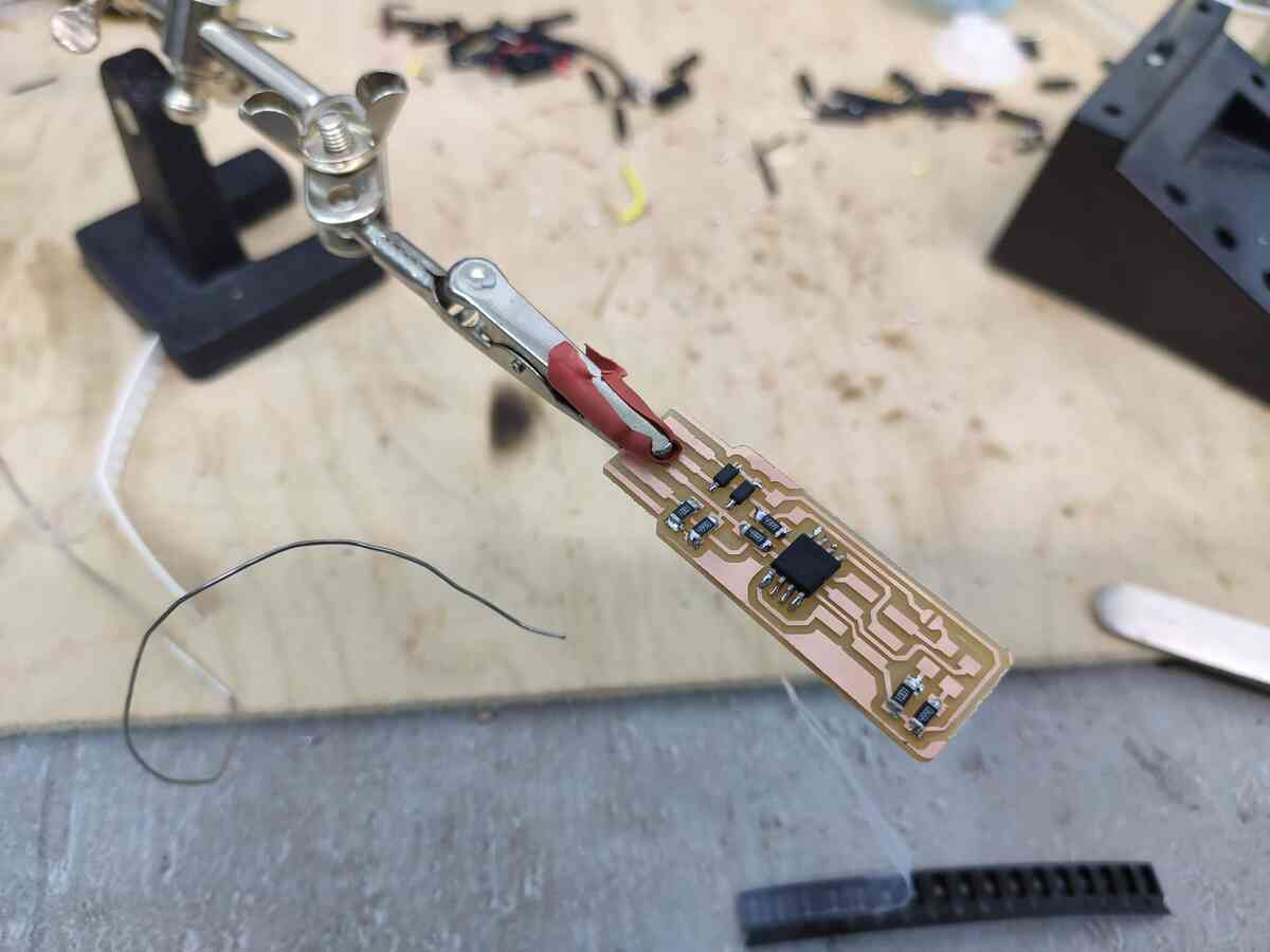
In order to stabilize the board for soldering, I used a holder with a piece of wire cover under the clip to avoid scratching the board. I didn't use any flux and used a traditional manual solder to solder on the components using a lead-based solder.
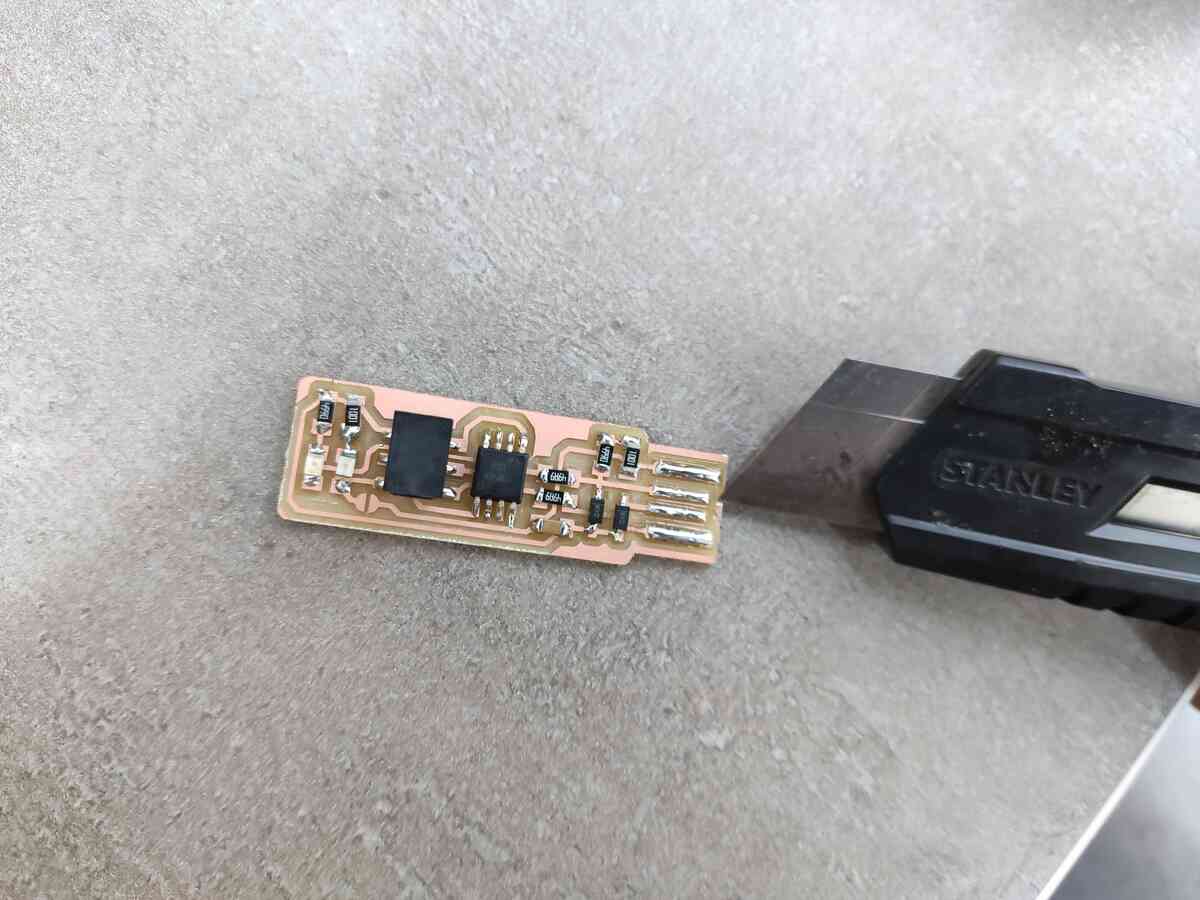
Once the soldering was done, the extra patch of copper was removed from the USB connection section not to cause any inadvertent shorts. I used a box-cutter for that:
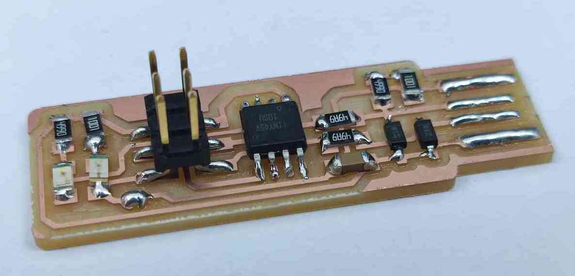
Lo and behold, here's my finished up FabTinyISP in all its glory including the bridge that connects VCC to Vprog minus the final programming:
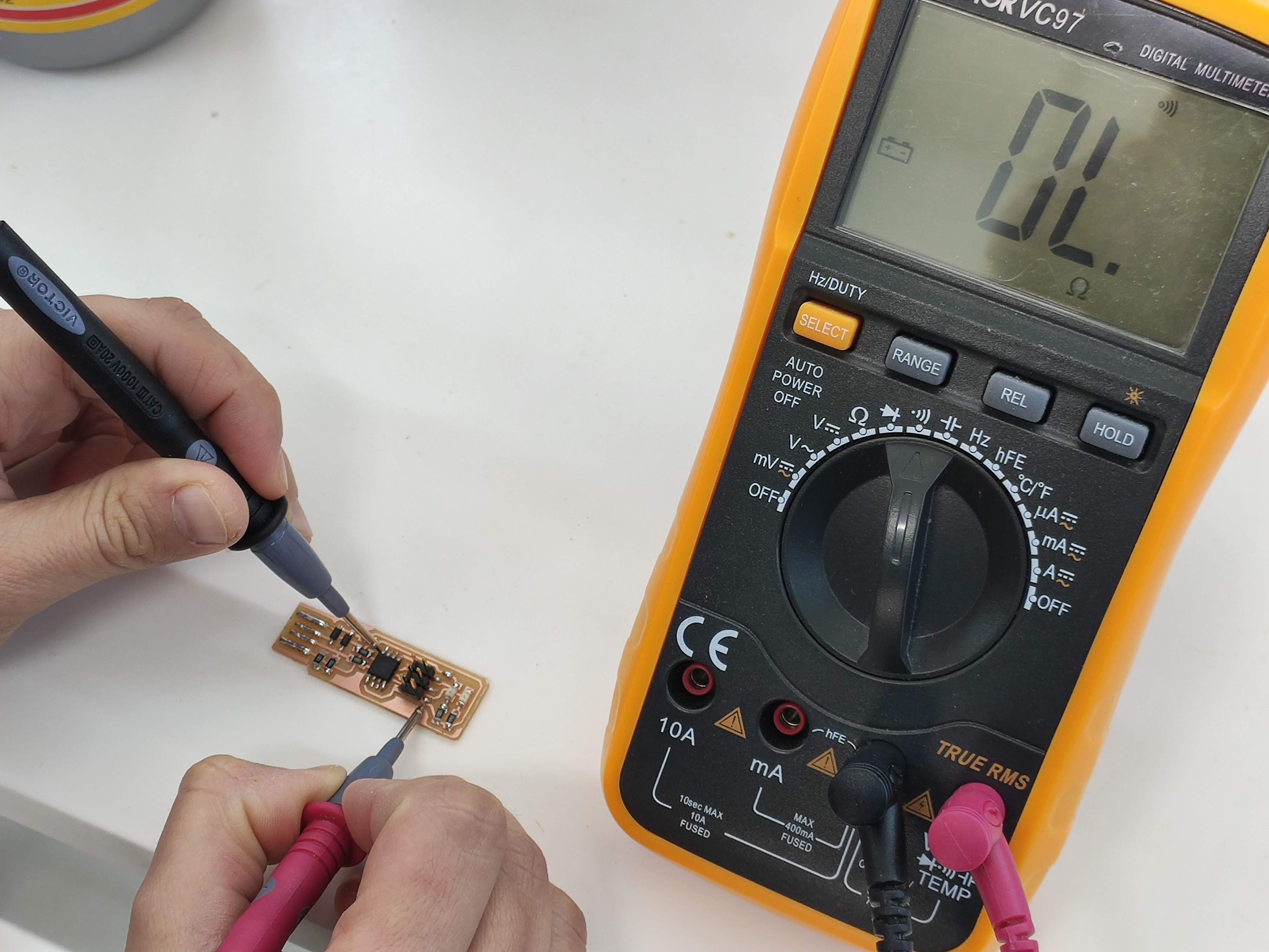
Before testing the board, I made sure that the VCC and GND were not shorted:
In order to program the FabTinyISP, I used the small transluscent blue programmer (as referenced in Brian's wonderful documentation).
The FabTinyISP had to be plugged in to a USB 2.0 port not to potentially damage the port, preferrably through a USB cable. I skipped the latter but used a USB 2.0 port. I must add that the USB connection was not very tight and if I plugged it in all the way, the red light would turn off, and the best spot for the connection was somewhere midway. After finishing the programming I added an extra layer of tape behind the board to give it slightly more thickness for a better USB connection.
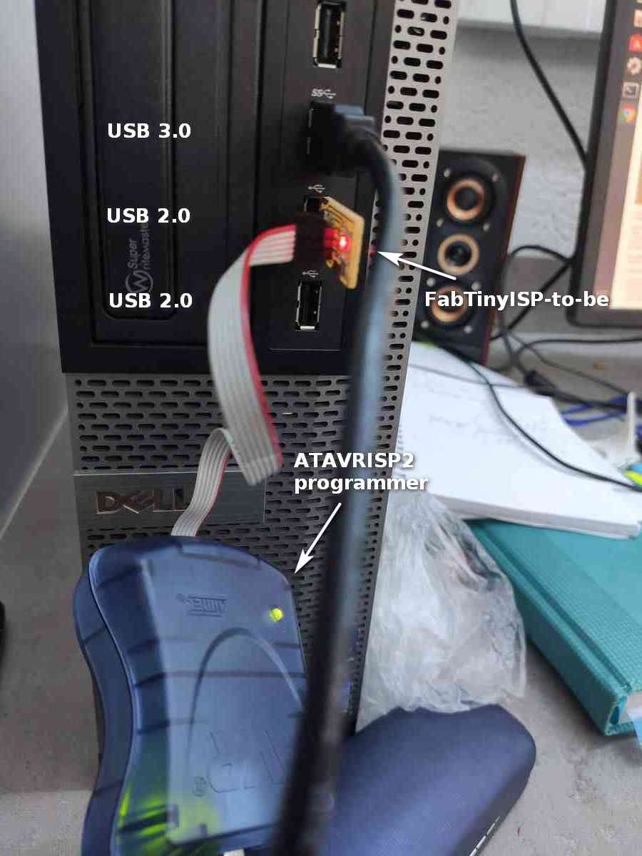
I used nano to edit the Makefile and input the programming device I was using. Initially, there was a hiccup in programming
as I input avrisp for the PROGRAMMER per what was printed behind the programmer itself. However,
I had to change that to avrisp2 per Brian's documentation for it to work:
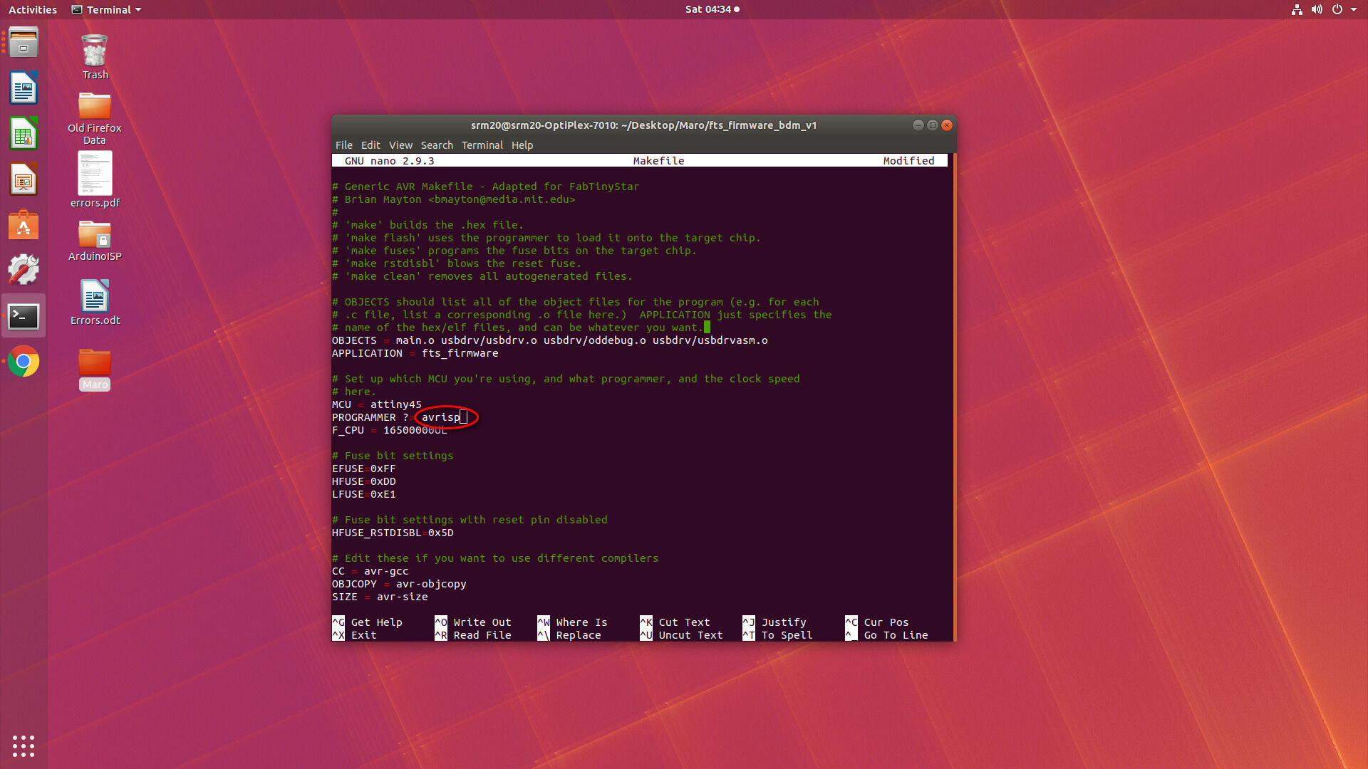
The programming, setting up the fuses, testing the USB functionality, and blowing the Reset fuse went smoothly.
After programming the board, the bridge connecting VCC to Vprog was removed using a copper wick and the solder. Here's a video showing how the programming bridge was removed using a wick and solder after the ISP was programmed and could be used to program other boards:
[In order to reduce the size of the video, the ffmpeg command was used to trim and then reduce the bit rate of the
video (the bit rate can be obtained by dividing the size of the target video in bits by the length of the video in seconds):
ffmpeg -i input.mp4 -ss 00:00:00 -to 00:00:18 -c:v copy -c:a copy output.mp4
ffmpeg -i input.mp4 -b 500k output.mp4
]
One problem the ISP had was that the board did not have enough thickness to provide a tight connection when the ISP was inserted into USB. I of course tried to solve it by using a tape in the back of the ISP and putting soldering lead on the USB tracks. However, according to Neil Gershenfeld the latter is not really needed, and in order to solve the thickness issue the best solution is to stick a piece of old credit card at the back of the USB connector section of the ISP.
The images for this week were once more processed with ImageMagick and the in-picture captions for this week's assignment were added using FastStone Image Viewer, which I'm slowly getting to know and enjoy.
Design rules
In order to assess the closeness of the traces that the machine can mill using the 1/64" milling bit, the following image was milled on a board to perform a line test:
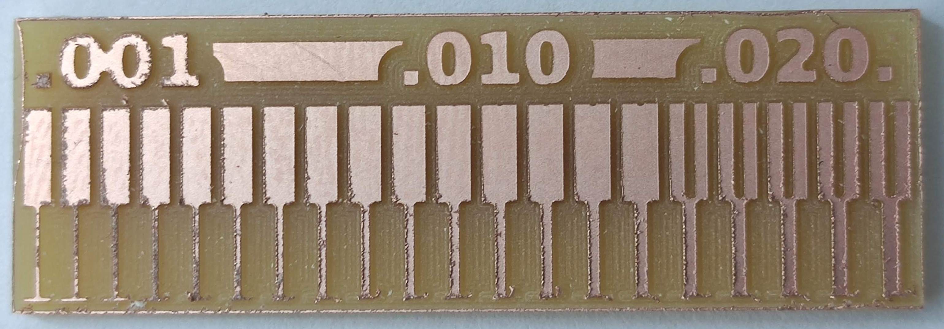
As can be seen from the test, when milling lines that are thinner than 0.001" from two sides, the mill can erase the line. See the jageddness around the thin lines to the left of the image.
And also the 1/64" mill cannot cut lines smaller than 0.016", which is to be expected as 1/64"=0.016". This can be seen in the fact that only the rightmost five lines are visible at the top half of the image, and the same line has failed to be milled in the rest using the 1/64" mill bit.
More about the test and the PCB design rules can be read at the Dilijan Fab Lab's 2021 website.
The G-code for the traces of the line test can be downloaded from here and for the outline can be downloaded from here.
Chirp
Emboldened by my experience with FabTinyISP, I attempted to make a capacitive humidity sensor PCB as described in the Chirp open project. This sensor is placed in the soil and starts to "chirp" (make a sound) when the soil humidity is low, reminding one to water their plants.
All the schematics and codes for the project are available on github.
I downloaded the files, opened the board with Eagle (which apparently comes with the same educational license as Fusion 360), and this is what I got:
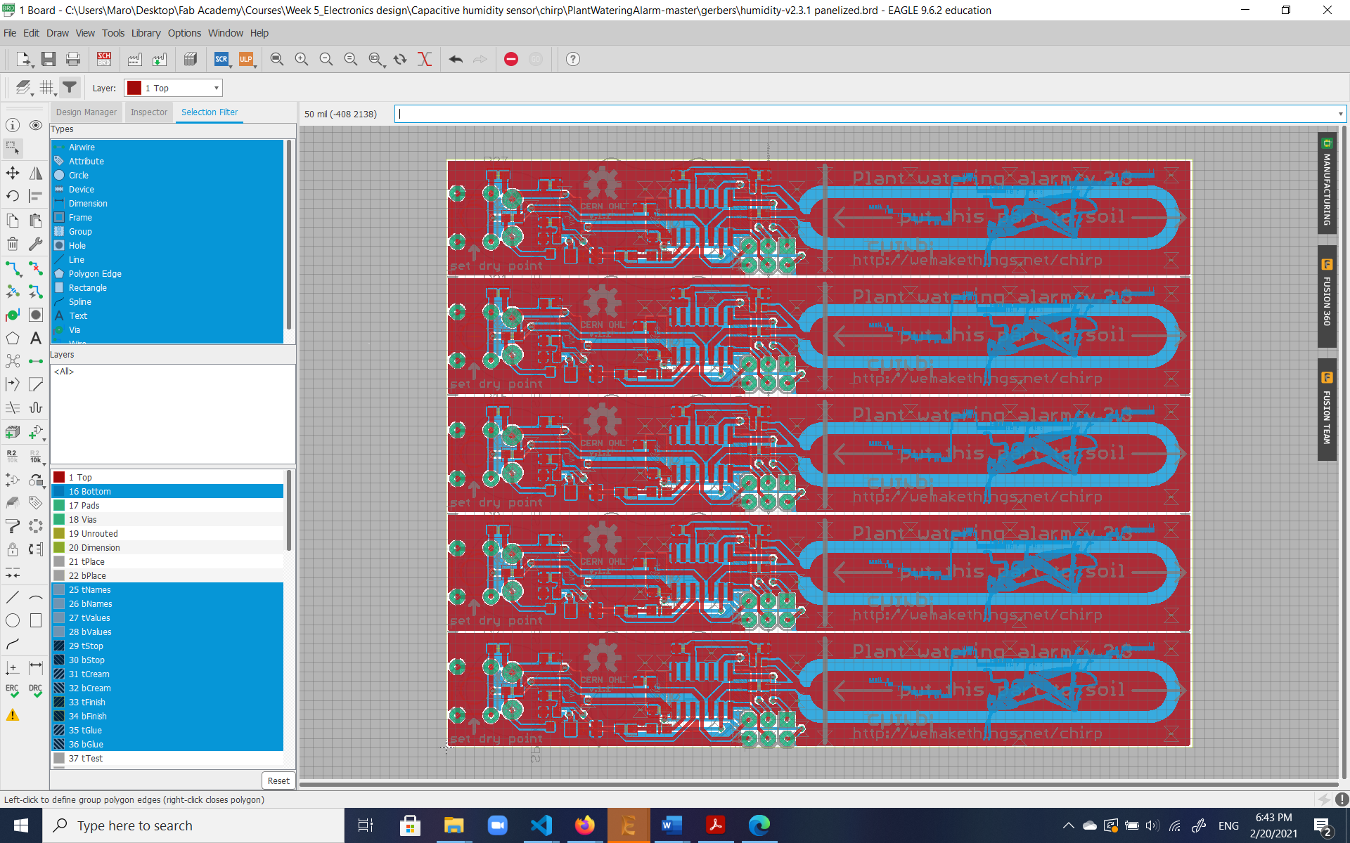
Confused by all the layers, I wanted to separate those belonging to the top and bottom of the PCB, and make individual png images of each. In order to made monochromatic png's for printing from the multilayer Eagle files, I used the following script that I found online:
DISPLAY ALL

                        RATSNEST

                        DISPLAY None

                        DISPLAY Top Pads Vias

                        EXPORT IMAGE C:\Users\Maro\Desktop\pcb_top.png MONOCHROME 1200;

                        DISPLAY None

                        DISPLAY Bottom Pads Vias

                        EXPORT IMAGE C:\Users\Maro\Desktop\pcb_bottom.png MONOCHROME 1200;

                        DISPLAY ALL
The script helped me to create the following:

Printing that resulted in the following:

Which was so off I started doubting I should've inverted the image. But one try later, and looking at the incomplete traces, my guess is that the spacings must be the problem as the bit is not able to reproduce the close/narrow traces, so ends up not engraving some of them at all.
This is a problem I'd like to revisit sometime in the coming weeks, especially after some tutorials in either KiCAD or Eagle and find out what went wrong.


