Individual project:
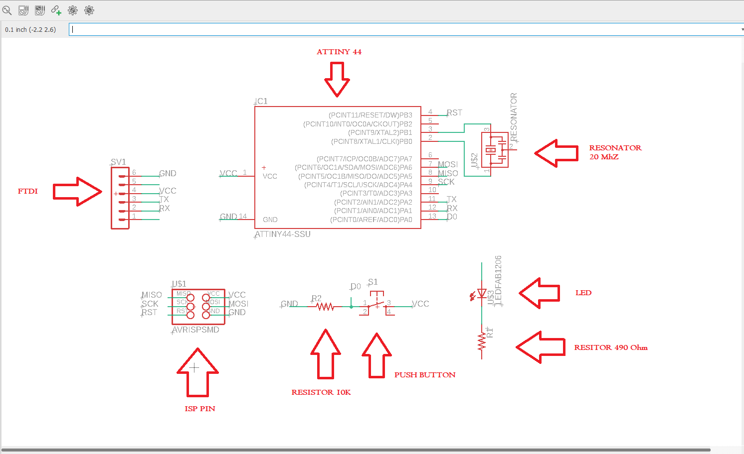
Redraw an echo hello-world board, add (at least) a button and LED (with current-limiting resistor) check the design rules, make it, and test it.
For this assignment I use Eagle software from autodesk which is an automated electronic design application.
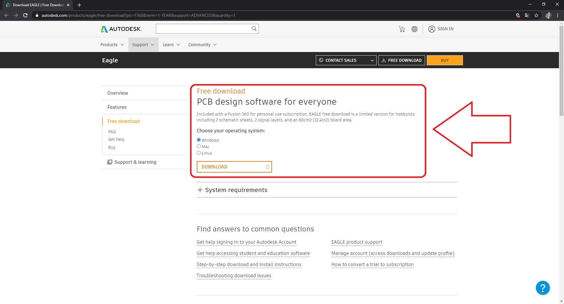
To start the practice first it is important to prepare the work environment for which we will initially download the software from the official Autodesk page. To download press Here
The installation process in the Windows operating system is very simple, you just have to run the installation file and follow the instructions.
Once the EAGLE software is installed, we have to import the libraries of the required components. For this we first download the library file in the following Link
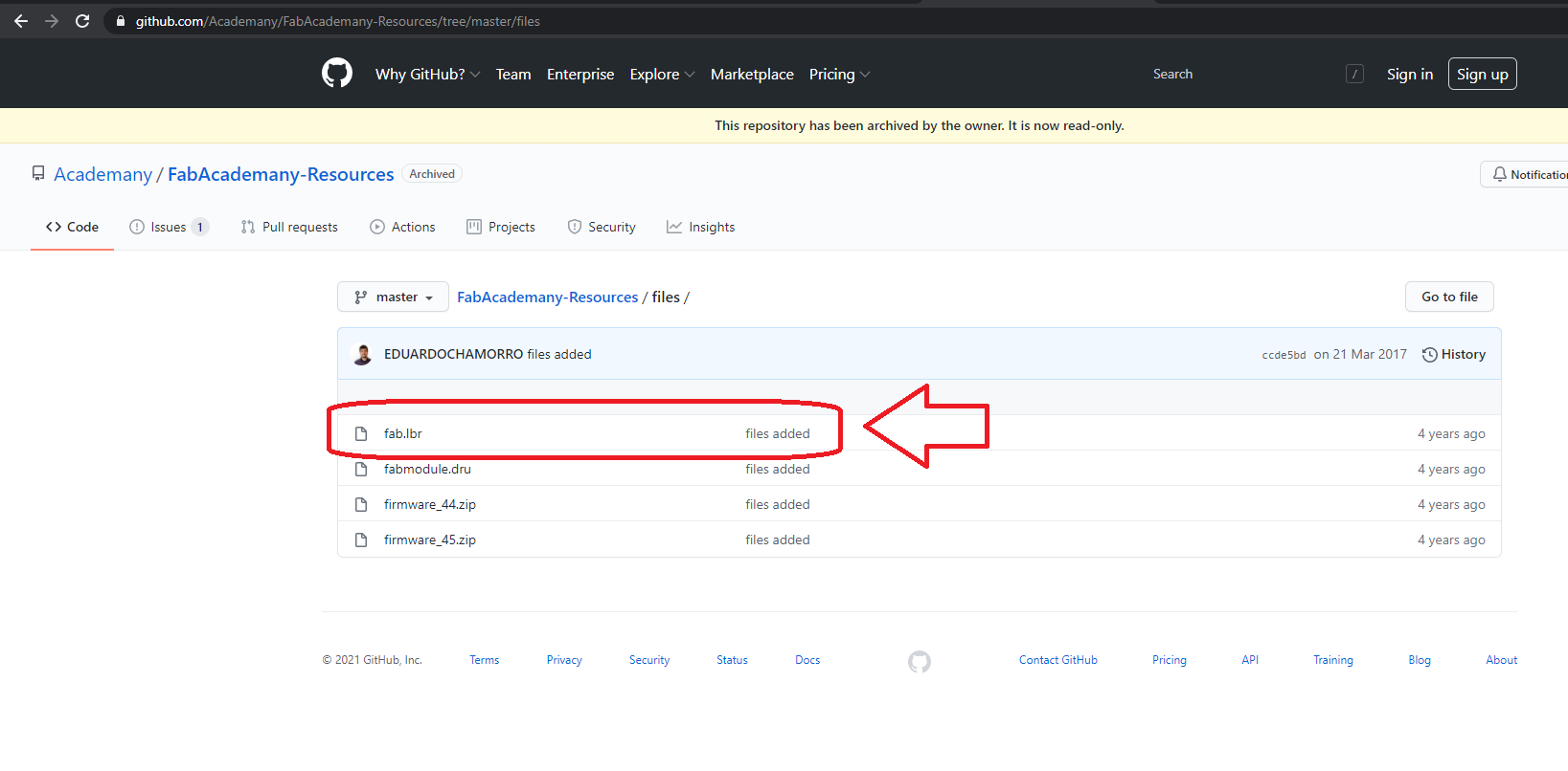
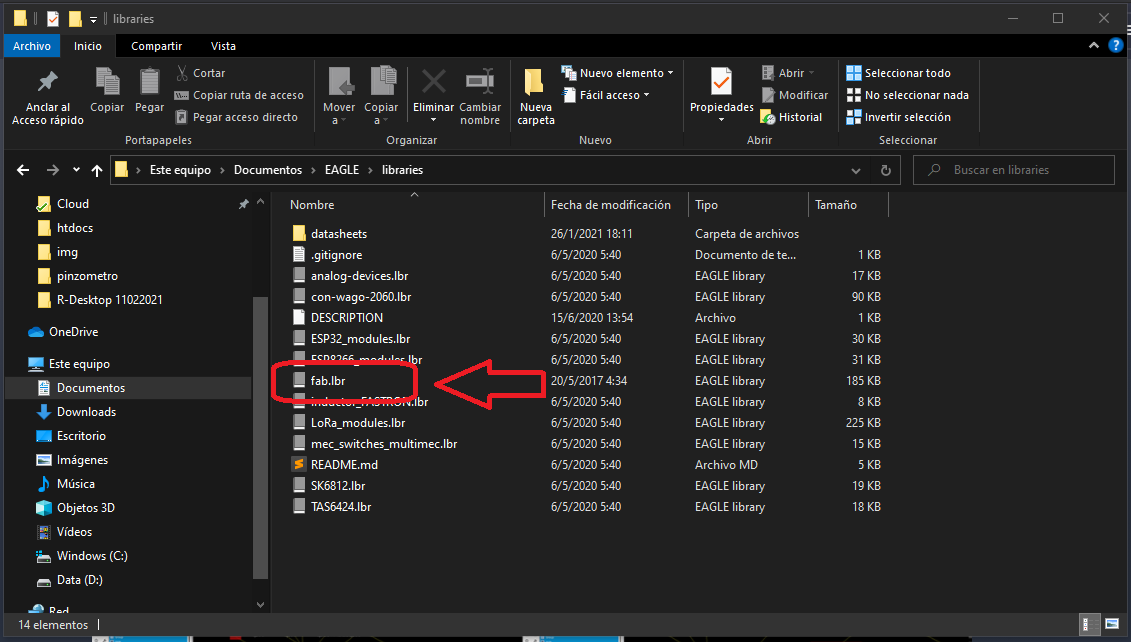
Once the file has been downloaded to install the library in our software, it is only necessary to paste the file in the following location ..\Documents\EAGLE\ libraries
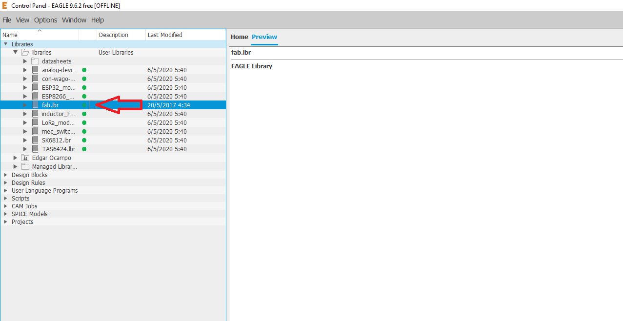
It is important to check that our library is activated before starting with the circuit diagram
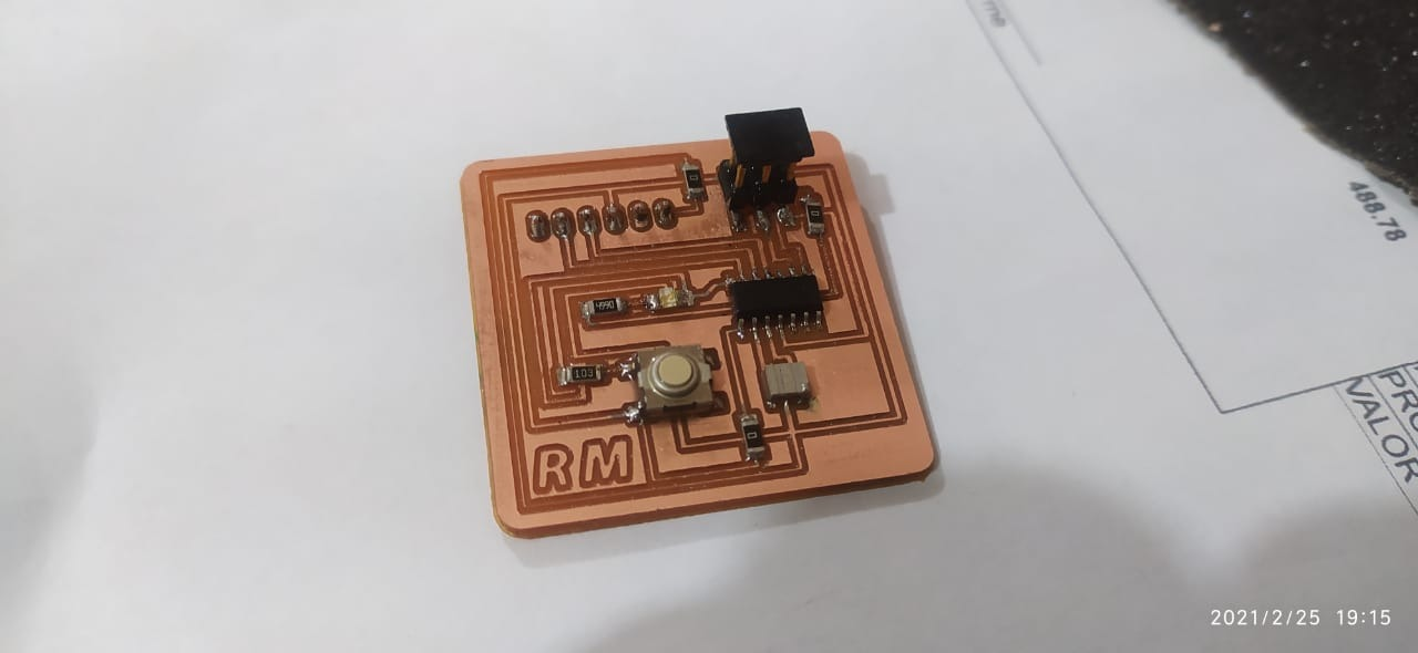
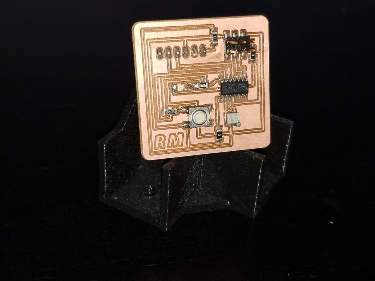
The following electronic components were used for the circuit
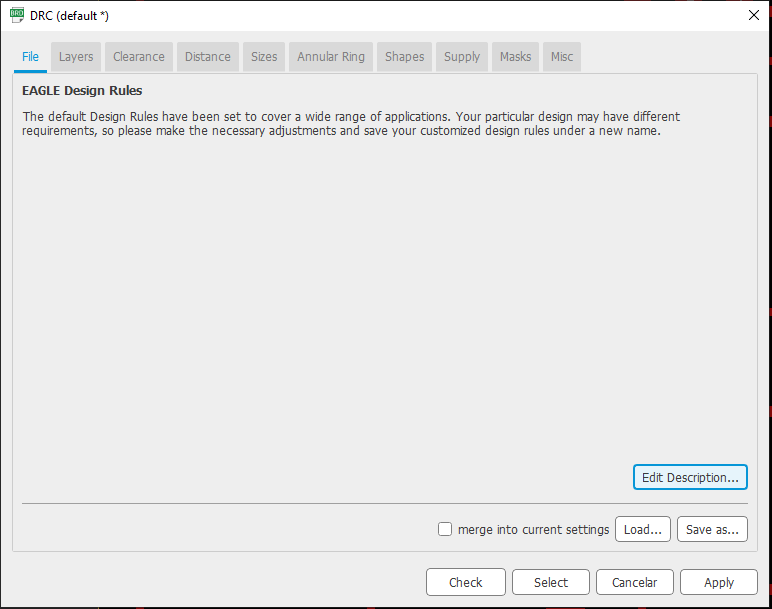
Design rules configuration
It is very important prior to the routing of the circuit tracks to configure the design rules, these allow us to verify that our design is within the production limits. For this, EAGLE offers us a tool that will inform us of any problem area to carry out production.
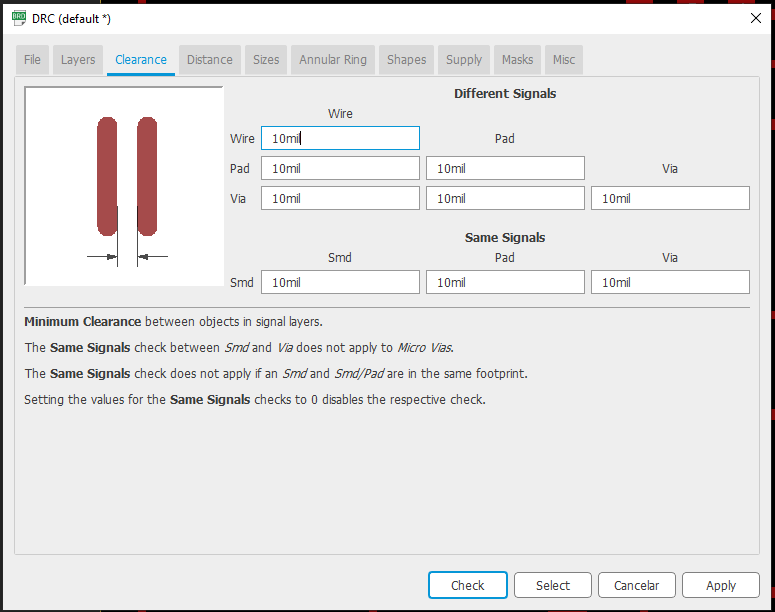
Spacing rules (clearance)
In the "clearance" tab we can enter the spacing that must exist between the "through hole" pads, SMD pads, vias and the tracks themselves.
Typically, PCB manufacturers working with small batches or individual printed circuits require a minimum pitch of 8 mils.
It is not necessary to explain much why the same software is showing us an image that illustrates the setting that we are going to modify.
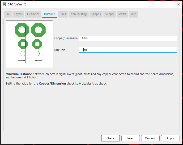
Distance rules (distance).
In this tab we can define the distance between the copper elements in the design (pads through hole, SMD pads, vias, tracks, etc.) and the outer edge of the PCB. For example, we can define if we do not want tracks less than 20 thousand from the edge (remember that the edge of the PCB is defined by the line in the "dimension" layer).
We can also configure the minimum distance between holes (holes) located within the PCB area.
Size rules (sizes).
In this tab there are two main settings to modify. For double-sided PCBs the settings that interest us are:
- “Minimum Width” that modifies the minimum size (thickness) of the copper tracks
- “Minimum Drill” that specifies the minimum diameter of the tool to make holes in the PCB.
The other two options presented on this page apply only to PCBs with more than two layers and will not be covered for now
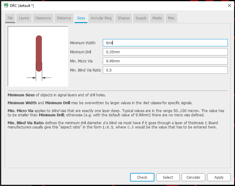
Again, here we must consider the maximum width of the track that we are able to achieve with the homemade method for manufacturing PCBs and also the minimum size of the perforations according to the tools we have.
Other settings.
- Shapes: Allows you to adjust the shape of the SMD and Through-Hole pads. For example we can round the pads of surface mount components or assign pads in different ways for the first pin of DIP packages.
- Supply: This tab allows us to make settings that define how the pads are connected to the power distribution layers, for example how the pads are connected to the GND or VCC polygons.
- Masks: In this tab we can configure how the program will generate the anti-weld mask layers. The default solder mask does not apply to tracks or pads.
- Misc: Here we will find various options on how the program performs the revision of the design rules, for example we can force the program to throw errors if the components are not aligned to the grid.
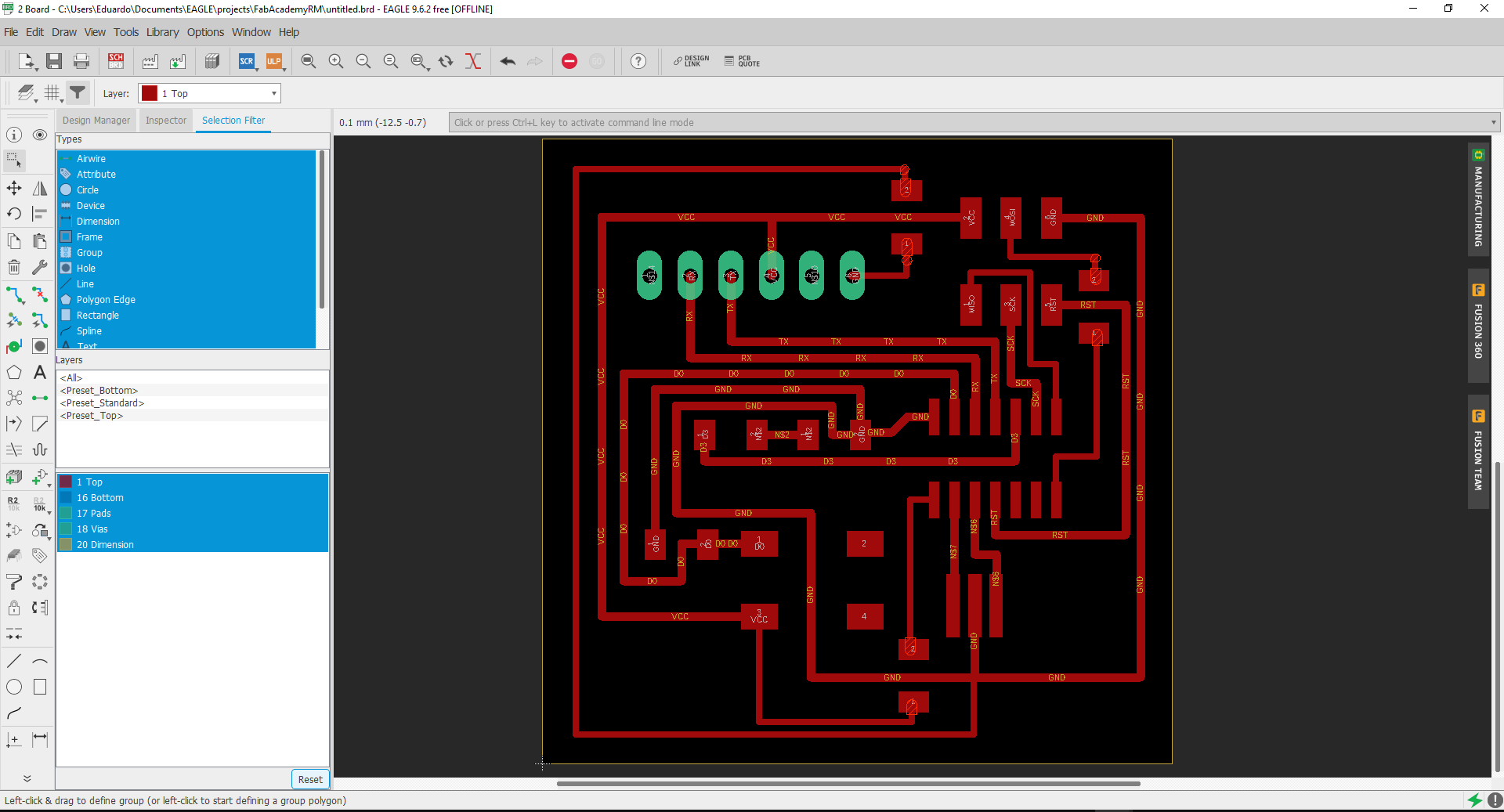
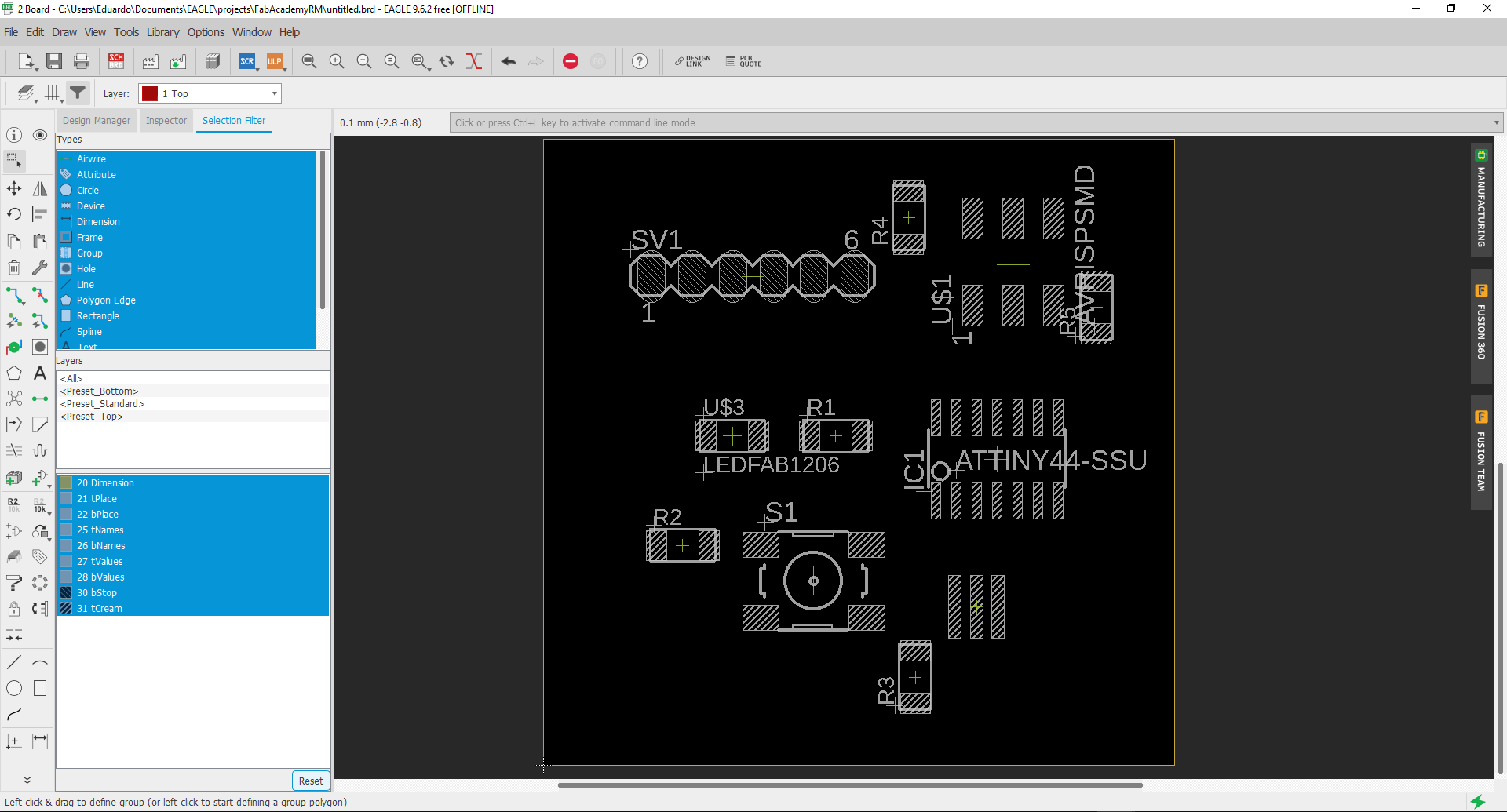
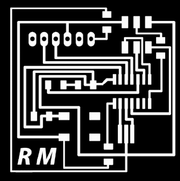
PCB layout
machining process
Due to the pandemic, it was not possible to attend the laboratory, however I was able to borrow a model 1610 CNC machine with which I could manufacture the PCB for this practice.
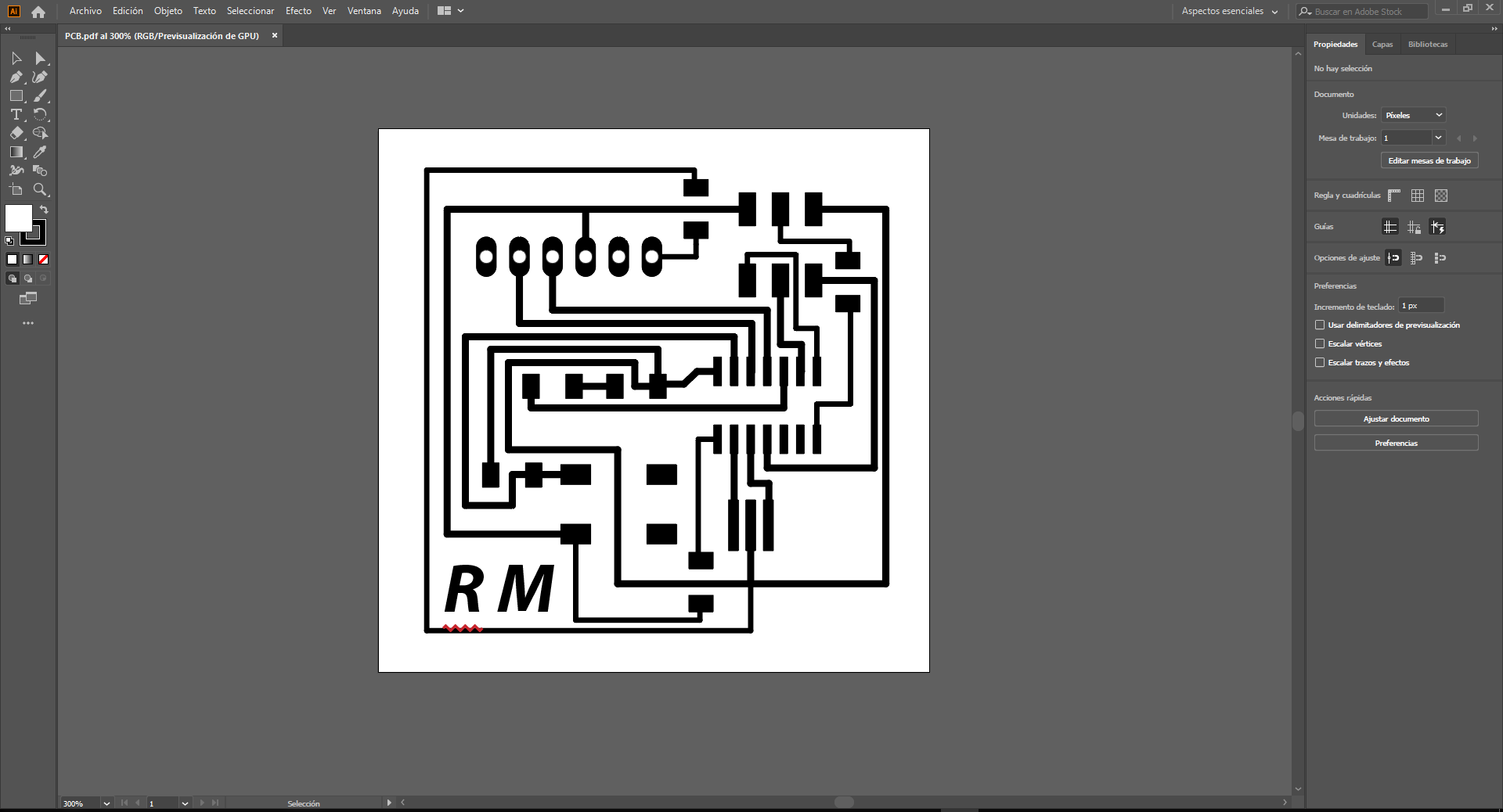
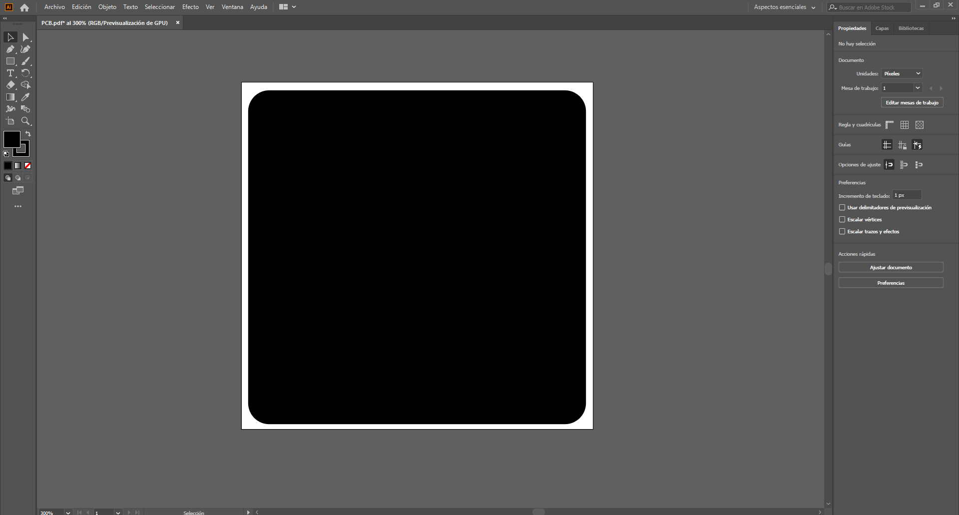
Once the design is done in the EAGLE software, download it in PDF format and then make some modifications in the Adobe Illustrator software. After this save the files for both cut and raster in PNG format.
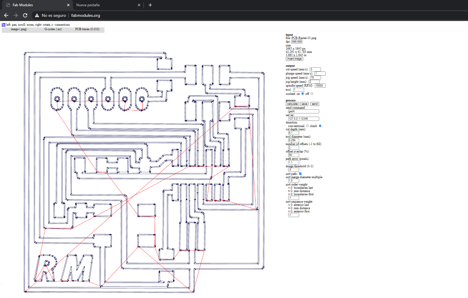
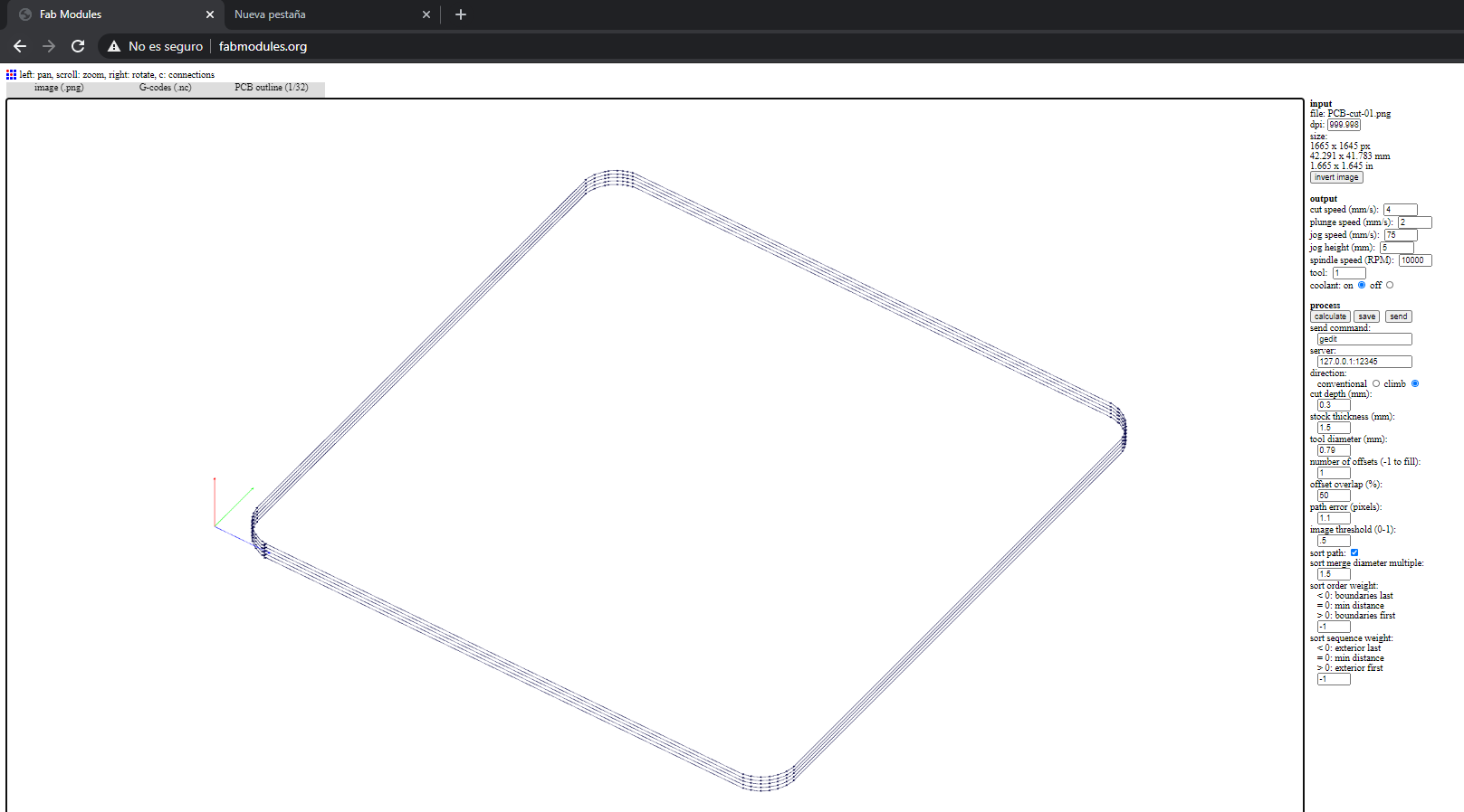
Raster and cutting file generation
Once the PNG files were obtained, the fabmodules tool was used to generate the cut and raster files in G-CODE format.
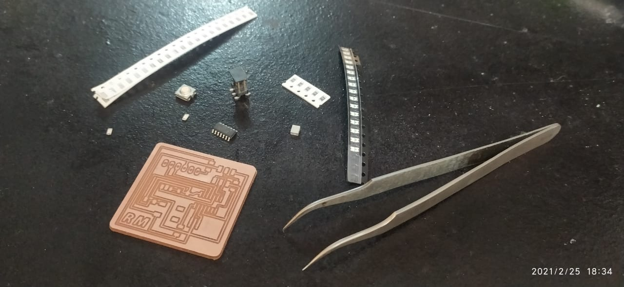
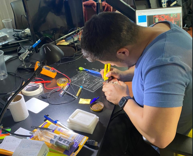
PCB manufacturing process and component soldering
For the manufacturing of the PCB, I used a replica of a Roland MDX-540 benchtop milling machine. It was loaned to me by a friend due to the pandemic. The milling machine was of great help in carrying out the manufacturing process accurately and efficiently.
Programming
int count;
// the setup function runs once when you press reset or power the board
void setup() {
  // initialize digital pin LED_BUILTIN as an output.
  pinMode(3, OUTPUT);
  pinMode(0, INPUT);
}

// the loop function runs over and over again forever
void loop() {

int button= digitalRead(0);

if(button == 1){
  delay(300);
 count = 1 - count;

  }

  if (count==1){
    digitalWrite(3,1);
    }else{
      digitalWrite(3,0);
      }

}
Test run
HERO SHOT
Conclusion
- Double check PCB tracks before applying power.
- When designing the tracks on the computer it is necessary to take it easy, for me this was one of the biggest drawbacks in this process.
- It is not necessary to be an expert in the use of digital tools, it is advisable to review the information of previous students who had similar problems.
- To make the cut in the CNC milling machine the best option is to do a test before applying the cut, especially if you have never used this machine before.
- After having several problems with programming I took the option of doing the programming in the Arduino simulator and this made the process much easier.