Exercise 14. 📱 Networking and Communications 💻 📝 📲
At the end of this exercise, I should be able to:
1. Send a message between two projects.
2. Design, build and connect wired or wireless node(s) with network or bus addresses.
3. Implement and interpret networking protocols and/or communication protocols.
4. Demonstrate and document workflows/processes used in network design.
In the previous exercises like input devices and ouput devices , I have used serial communication between MCU and the target devices.
To gain a better understanding on serial communications especially UART, I2C and SPI Serial communications I spend some time watching these videos
1. Overview of UART - I2C - SPI.
2. I2C communication and how to use it with Arduino.
3. SPI basics for beginners.
4. I2C protocols between 2 Arduino boards.
After watching these videos, I have better understanding on the serial communication and decided to use the I2C for this exercise.
Some key information on how I2C works are listed below:
a. An I2C bus has two signals, along with a power and ground connection. The two signal lines are: 1) SDA – This is the bidirectional data line and 2) SCL – This is the clock signal.
b. There are two types of devices that can be interfaced to the I2C bus – Masters and Slaves.
c. The Master device controls the bus and supplies the clock signal. It requests data from the slaves individually. There can be more than one master device on the bus but only one can be the active master at any given moment. The master devices do not have an address assigned to them.
d. Slave devices do have an address, and this address needs to be unique on the bus. Multiple slaves devices can be on one I2C bus.
e. Arduino IDE has a built-in library for working with I2C called the Wire Library. It can configure the Arduino to become either a master or a slave.
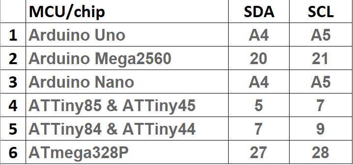
f. The SDA and SCL connections for I2C are different between MCU models. Below are some of the pin connections for some of MCU/chips:
📱Send a message between two projects (Group assignment)
For this exercise, we decided to use various types of communications using Arduino boards such as:
1. SPI using 2 Arduino Uno boards.
2. UART using 2 Arduino Uno boards.
3. Bluetooth between Arduino board with bluetooth module and mobile phone.
The details can be seen HERE.
📝Design, build and connect wired or wireless node(s) with network or bus addresses💻
For this individual assignment, I did 2 attempts:
1. I2C bus communication using my own board, ATMega328 and an Arduino board.
2. I2C bus communication using my own board, ATTiny45 and an Arduino board.
1. I2C bus communication using my own board, ATMega328 and an Arduino board.
I started to use the board that I have made for MY FINAL PROJECT that uses ATMega328 and connect it to Arduino UNO board to communicate using I2C bus.
To recall, below is the schematic and board design that I have made.


The SCL pin is PC5 and SDL pin is PC4 which are exactly the same as Arduino board.
to download the EAGLE schematic .sch file
to download the EAGLE board .brd file
to download the .png file of the traces.
to download the .png file of the board cutout.
I followed this tutorial on arduino site which is quite simple.
The ground for the arduino must be connected to the ground of the ATMega 328 board.
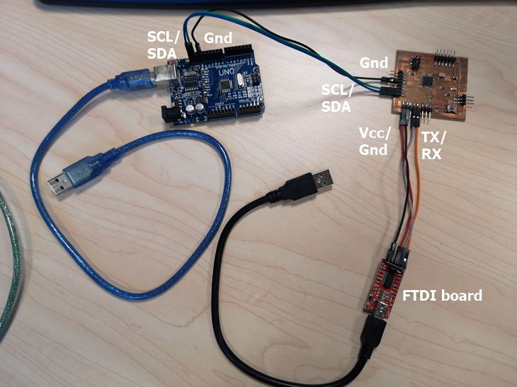
The ATMega 328 board is connected to an FTDI board to display the serial monitor by using the TX/RX pins on the board connected to the RX/TX pins of the FTDI board. At the same time the VCC and GND of ATMega 328 board is connected to the VCC and GND of FTDI board for power supply where the FTDI board will be connected to a PC via USB connection.
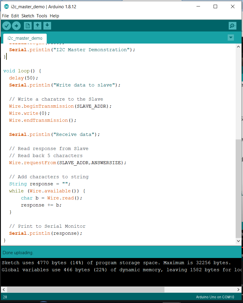
Here, ARDUINO board will act as a master that will be programmed to request and then read data from slave.
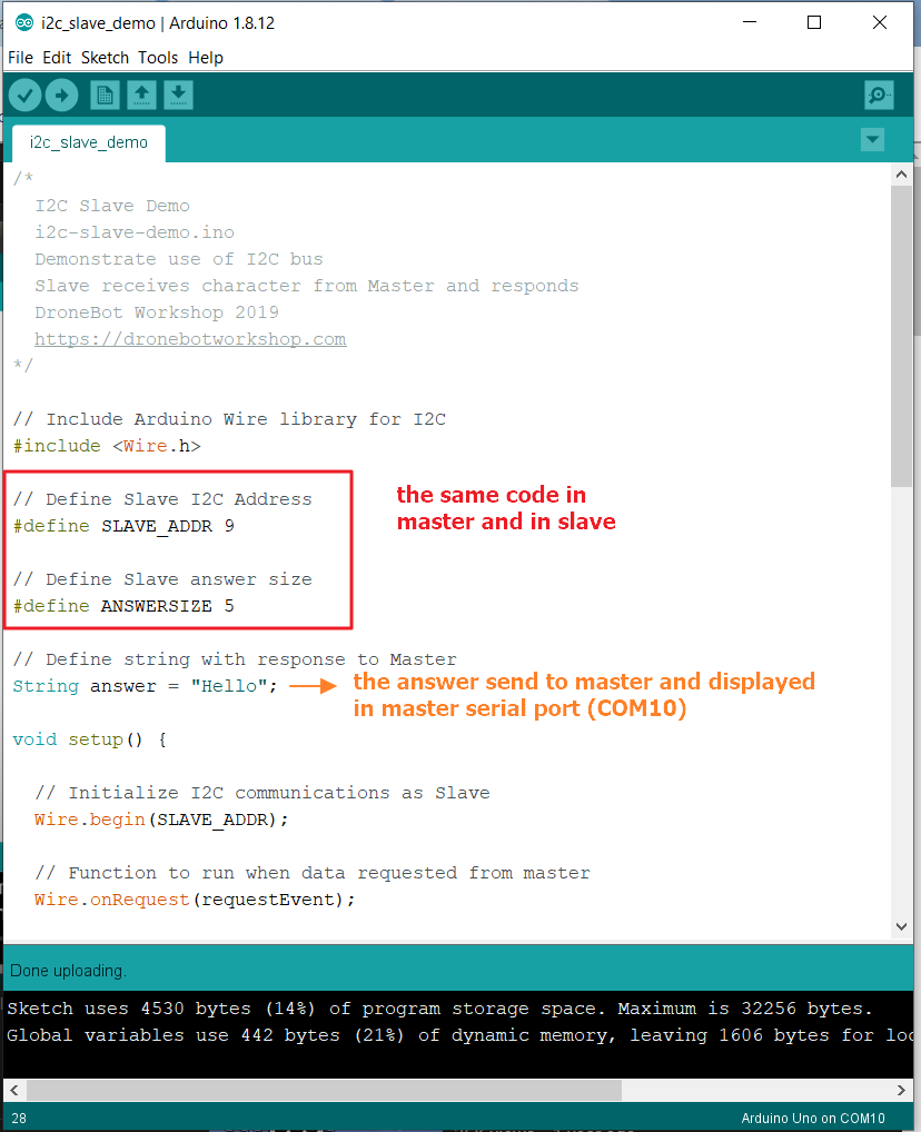
While my ATMega328 board will act as a slave.
The slave will receive the request from the master and send the data "Hello" to the master.
The Arduino sketch code use for the Master is shown below:
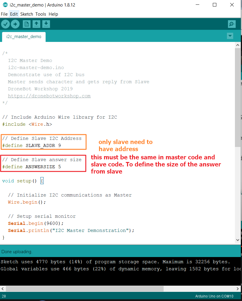
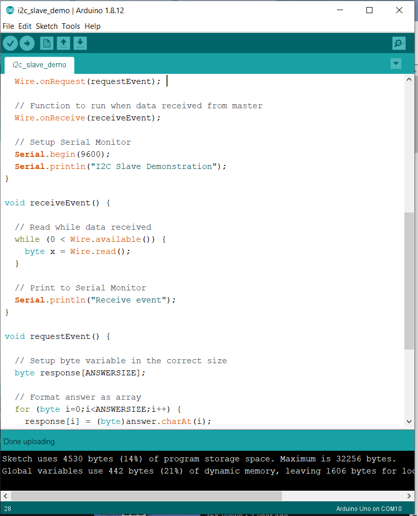
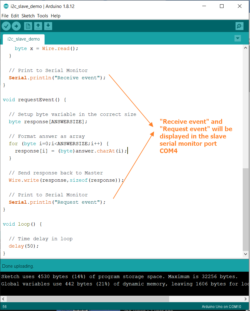
While the arduino sketch code for the slave is shown below:
to download the "MASTER" sketch code
to download the "SLAVE" sketch code
The data sent from slave can be read in the serial monitor of the master (In this work, the master serial port is COM 6)
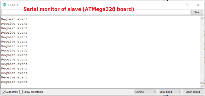
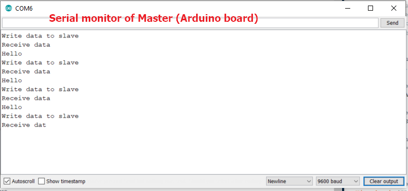 The 2 pictures above are the serial monitor of the slave (ATMega328 board) and the serial monitor of the master (Arduino board).
Below is the short video when the 2 boards communicates via I2C bus.
2. I2C bus communication using my own board, ATTiny45 and an Arduino board.
With this gained confidence, I started to use the board that I have made for Exercise 6. Electronics Design that uses ATTiny45 and connect it to Arduino UNO board to communicate using I2C bus.
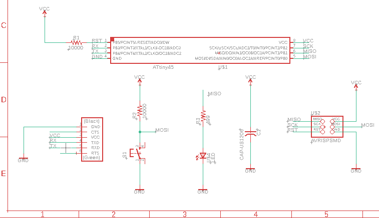
To recall, below is the schematic of the board that I have made.
to download the schematic file drawing in EAGLE
to download the board file drawing in EAGLE
to download trace.png file
to download cut.png file
I used ATTiny 45 as the MCU on this board and the dedicated SDA is pin 5 and the dedicated SCL is pin 7.
I design the board as such that pin 5 is connected to push button and the 10k pull-up resistor. While pin 7 is not used after programming (It is only used as SCK during programming when connected to ISP programmer).
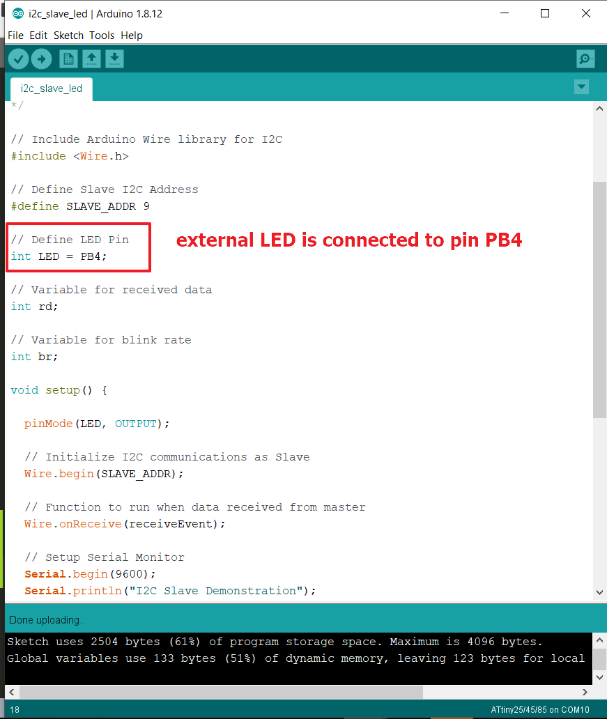
While the LED is connected to pin 6 (PB1)
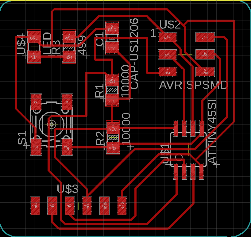
And below is the board design.
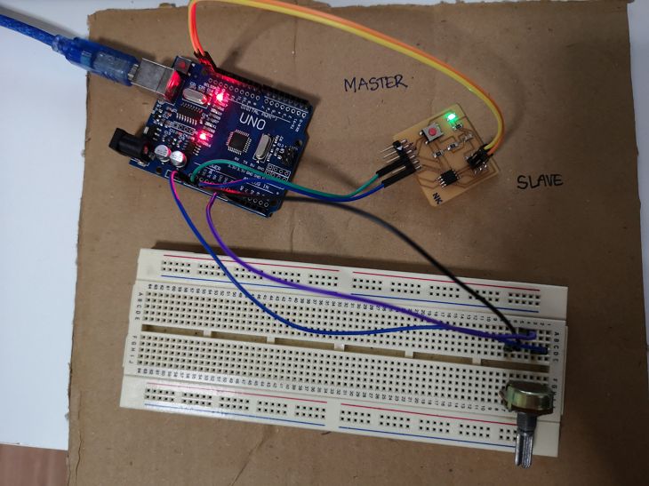
For this experiment, I want to hook a potentiometer to the master Arduino board and the LED on the ATTiny45 board will blink accordingly. I will use the potentiometer to control the blink rate of the LED.
Here's how I connected the potentiometer to the arduino board and connect the SDA/SCL pins on Arduino board to the SDA/SCL pins on ATTiny 45 board. I power the ATTiny 45 board using the 5V pin from Arduino via the FTDI pins.
Below are the arduino sketch code uploaded to the master (arduino board).

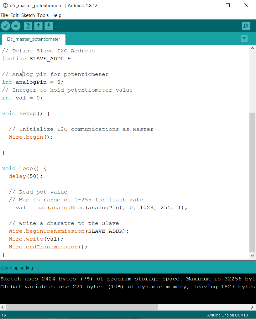
The sketch for the master side is simpler than the previous one. This is because I am just sending data to the slave.
Below are the arduino sketch code uploaded to the ATTiny 45 board (slave). For this, I set the clock speed of the ATTiny45 to be 16 MHz instead of usual 8 MHz.
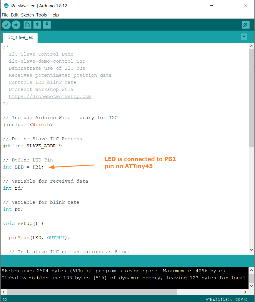
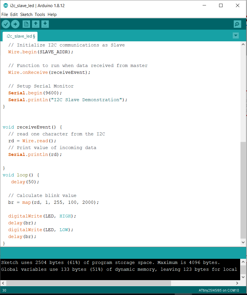
The slave side needs to receive data from the master and use it to flash the LED.
to download the master sketch code for Arduino board
to download the slave sketch code for the ATTiny45 board
After uploading the master and the slave code to Arduino uno board and ATTiny45 board respectively, I connected the 2 boards and powered them. But I observed that the blinking rate of LED is not affected by the potentiometer as shown in the video below.
I suspect it's the SDA/SCL connections that were not working properly.
I also tried to connect an external LED to pin 3 (PB4) of the ATTiny45 and control the blinking of that LED via the potentiometer connected on Arduino uno board and communicate this to the ATTiny 45 board via I2C. Below is the connection and the modification in arduino sketch code for the slave.
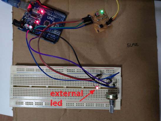
But the same thing is observed where the blinking rate of this LED is not affected by potentiometer too as shown in the video below.
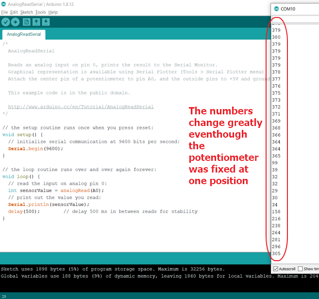
I tested the potentiometer using this simple arduino code and connections following this tutorial and it turned out that the potentiometer is spoilt as shown below where I should see a steady stream of numbers ranging from 0-1023, correlating to the position of the potentiometer. When the potentiometer is not turned, the number must remain constant, which is not the case as shown here, the numbers changes greatly. With this, I learnt that we need to check all the electronics parts individually before integrating all of them together.