A5
Electronic Production
Nowadays, the electronic components are almost everything for interaction, movement, and automation.
New and improved circuit layers are found everywhere, the most important thing in here, is HOW TO CREATE, HOW TO IMPROVE AND HOW TO PROGRAM THEM.
With this week assignment, we used a common png file to mill/engrave, solder and test a piece of board.
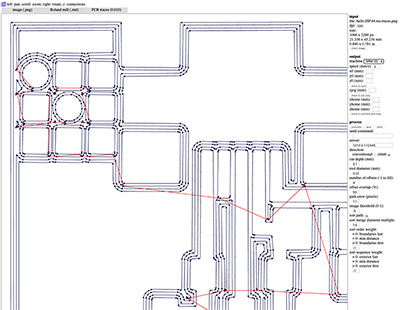
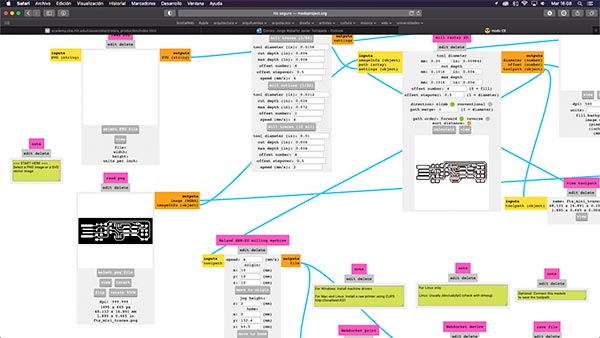
Using Fabmodules.org, and mods to figure out the actual process, to understand how the engraving works to ensure the leanest product.
After understanding the engraving paths, i realize about how to put the board.

With Fabmodules, is quite easy to assign the image, the process and the machine.
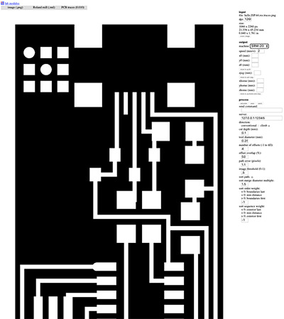
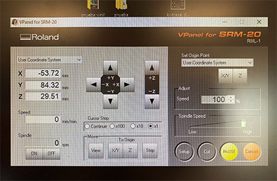
Now, for the calculation, we used 4 oofset steps, at speed of 2, with just 0.1mm depth.
X,Y,Z is on zero.
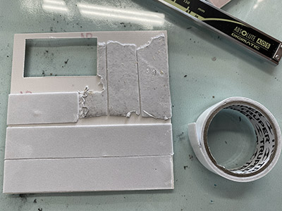
I had to calibrate the board to set the floor and have a better starting point.
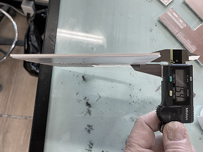
I used a recycled board to optimize material and avoid waste.
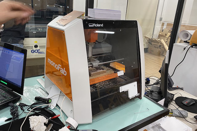
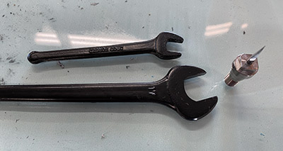
The wrench and drill to set the engraving machine.
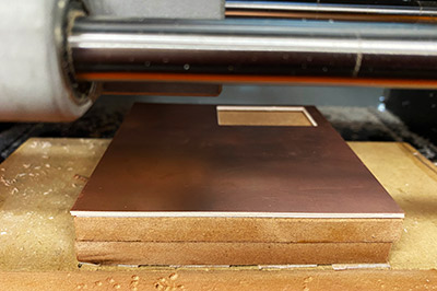
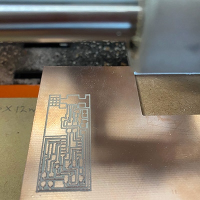
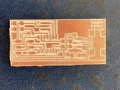
The board set in place, ready to be engraved.
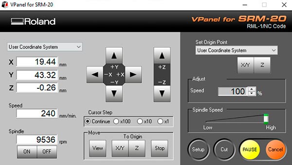
The V-Panel ready to "print".
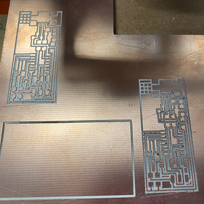
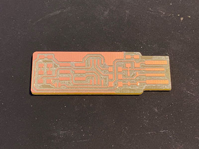
The piece already finished
A second piece correcting certain angles and joints.
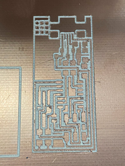
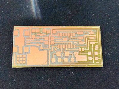
A close up form the board ready to be trimmed for the electronic production.
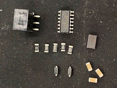
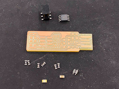
Next, following the png file with the soldering and setting instructions, y took all the necessary pieces to be atached to the board.
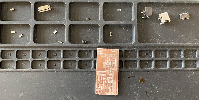
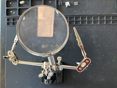
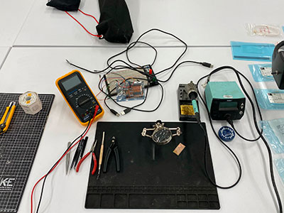
With a little help from mechanical tools, i started soldering this next pieces:
-Atiny44
-Crystal
-10k res
-1k res
-499 res
-10pf capacitor
-C3 Diode
-J1 ISP
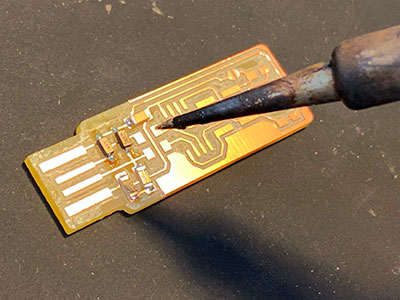
This is the process of soldering
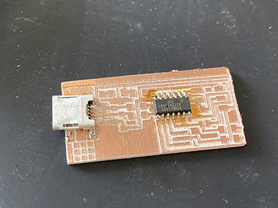
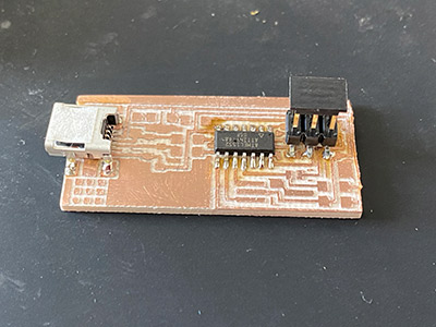
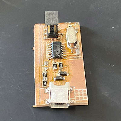
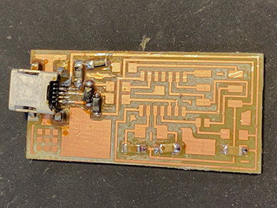
This is the finished PCB (first attempt)...
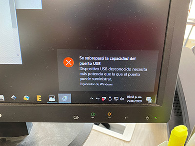
Finally, a test... bad test, beacuse we need some improvements, the PCB is NOT working.
Then, pandemic hit the world and i decided to start all over again, now in 2021... finding time to do a new PCB and use our brand new FabLab.
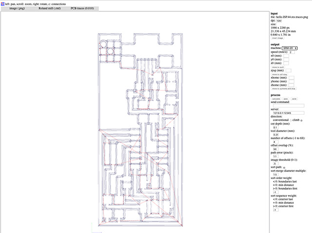
So, with a regular set with MODS (the new one that looks awesome).
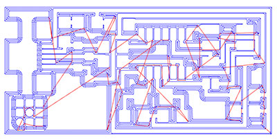
The new traces has been set and ready to be milled.
Second chance and a better place to work with it, cleaning a little bit the copper and settings parts.
Again, choosing the pieces:
-Atiny44
-Crystal (flat new one)
-10k res
-1k res
-499 res x2
-10pf capacitor x3
-C3 Diode x2
-J1 ISP (solder)
Dealing again with soldering and trying not to do a mess.
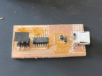
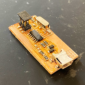
The "finished" product v 2.0, however, i found out that needed improvement, so i started all over again with another PCB...
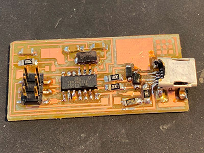
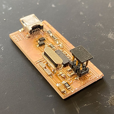
This is version 3... a USB type PCB, to see how it works.
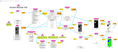
Again, using the new http://modsproject.org program, is quite easy to find and create the inputs.
Traces in orther to be sent to the milling machine, and the tolerances used to mill it in the Roland.
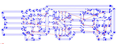
A cleaner better traced board.
An here i have a new PCB board, a little bit neat and with different components:
1x ATtiny45 or ATtiny85
2x 1kΩ resistors
2x 499Ω resistors
2x 49Ω resistors
2x 3.3v zener diodes
1x red LED
1x green LED
1x 100nF capacitor
1x 2x3 pin header
Now soldering with a lot more care.
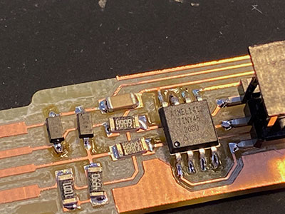
Little by little the pieces got together with a better quality
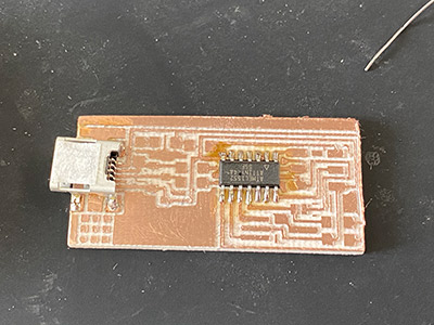
A close-up of how pieces fitted greater than before with the right orientation
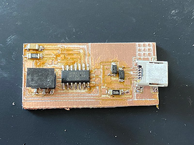
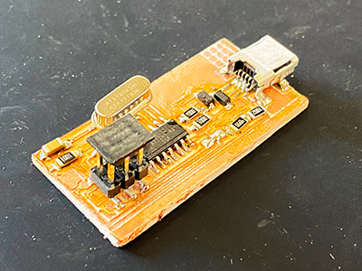
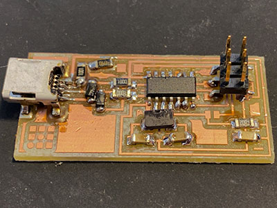
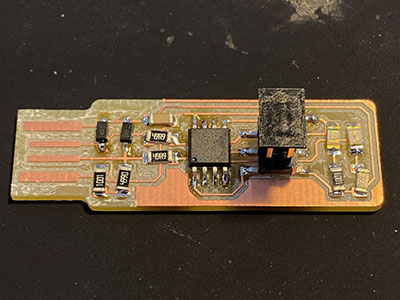
The finished PCB
And with a sad little secret... i put the first processor with wrong orientation, so i have to redo the whole PCB, but i achiveved a better excersise and a better finished product.
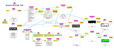
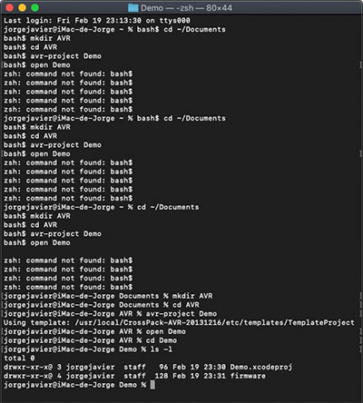
Then, i had the chance to do some further reading to understand once and for all how to program the PCB
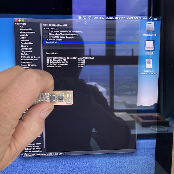
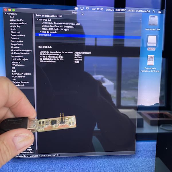
Testing the connectivity in-between USBtiny and computer
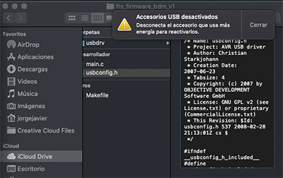
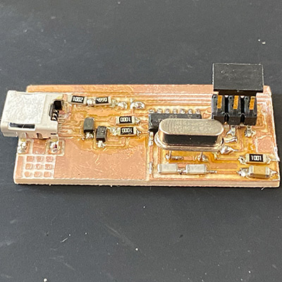
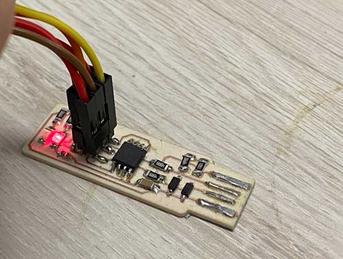
Finally i had the chance to debug and create files for programming in a working PCB!
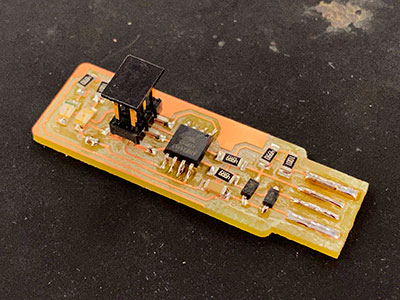
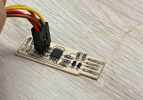
A working PCB!, took me a while, but it's done
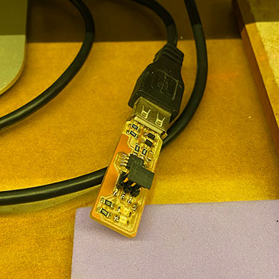
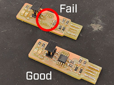
This PCB's are variants of the original to see the proper connectivity and electric flow... thanks to this process, i had the chance to see how things work with an ATTINY 45
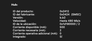
And finally, after so much struggle (at least for me) the ISP is recognized by the computer