Jose Alegria - Fab Academy
![]()
![]()
![]()
![]()
Electronics
Design
Assignment
wHAT iS THE ASSIGNMENT ABOUT?
Redraw one of the echo hello-world
boards or something equivalent, add (at least) a button and LED (with
current-limiting resistor) or equivalent input and output, check the design
rules, make it, test it. Optionally, simulate its operation.
GROUP ASSIGNMENT:
Use
the test equipment in your lab to observe the operation of a microcontroller
circuit board.
What did I learn:
-
The most important part of electronics
production is electronics design.
-
There are a few options to make the
design, this is the simplest part. Once you get used to design in the chosen
software the process is straightforward.
-
The difficult part is to connect all
the pins, ports, and pads correctly and getting to know the function of each
one of those.
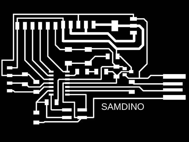
1st Step. Getting
a design
For this
assignment we are not making a board from scratch. So, I used the board that
Adrian Torres (Leon, 2020) uses as a SAMDINO,
to have a starting point and proceed with the modifications needed.
This is the
board I will be modifying:
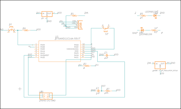
2nd Step.
Modifying the board
To modify the
board, I used the Eagle module embedded within Fusion 360. I made a list of the
components needed according to the first board, and then added the components
needed to install two sets of button and LED. The first one using the
microprocessors internal resistor and a second one using an external resistor.
|
Description |
Part |
Value |
Device |
Package |
Qty. |
|
Capacitor 1 micro F |
C1 |
1uF |
CAP_UNPOLARIZEDFAB |
C1206FAB |
2 |
|
Regulator 3.3 V |
IC1 |
VR_REGULATOR-SOT23SOT23 |
SOT23 |
1 |
|
|
Regulator 5 V |
LM2940 |
VR_REGULATOR_SOT223 |
VR_REGULATOR_SOT223 |
SOT223 |
1 |
|
Resistor 100 K |
R1 |
100 K |
RES-US1206FAB |
R1206FAB |
1 |
|
Resistor 0 |
R2 |
0 |
R1206FAB |
R1206FAB |
2 |
|
Resistor 1 K |
R3 |
1K |
R1206FAB |
R1206FAB |
2 |
|
Resistor (US Symbol) |
R7 |
10K |
R1206FAB |
R1206FAB |
1 |
|
Button 6 mm |
S1 |
6MM_SWITCH6MM_SWITCH |
6MM_SWITCH |
2 |
|
|
LED |
U$2 |
LEDFAB1206 |
LEDFAB1206 |
LED1206FAB |
2 |
|
Programming Pin 2x2 |
U$1 |
PINHD-2X2-SMD |
PINHD-2X2-SMD |
2X02SMD |
1 |
|
Microprocessor |
U1 |
ATSAMD11C14A-SSUT |
ATSAMD11C14A-SSUT |
SOIC14_SL_MCH |
1 |
|
USB Connectors |
X1 |
CONN_USBPCB |
CONN_USBPCB |
USB-A-PCB |
1 |
I changed
some of the component’s footprints to the ones in the Fabacademy Library to get
bigger footprints that are easier to fix to.
Then, the
next step was to create a board schematic with all the connections needed for
the board to work.
This is the
result:
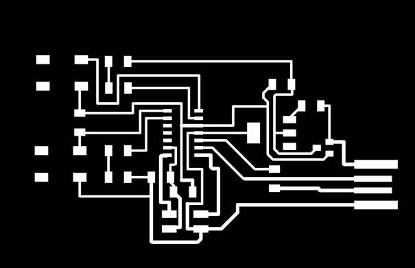
At last, I
had to locate all components in the PCB Board and make the routes needed to
connect them.
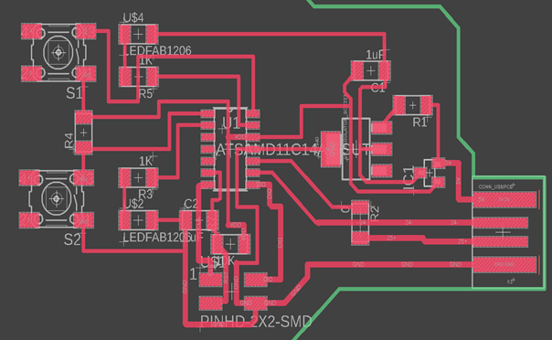
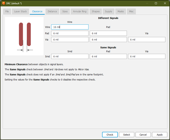
To
make the new routes I followed a few design rules such as:
1.
Minimum wire width: 24 mil (made this
way to avoid wire breaking up)
2.
Clearance: 16 mil (this is the tool
diameter)
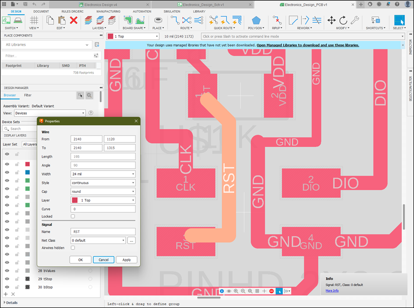
This
design rules that I followed by myself had to be set into the program in a
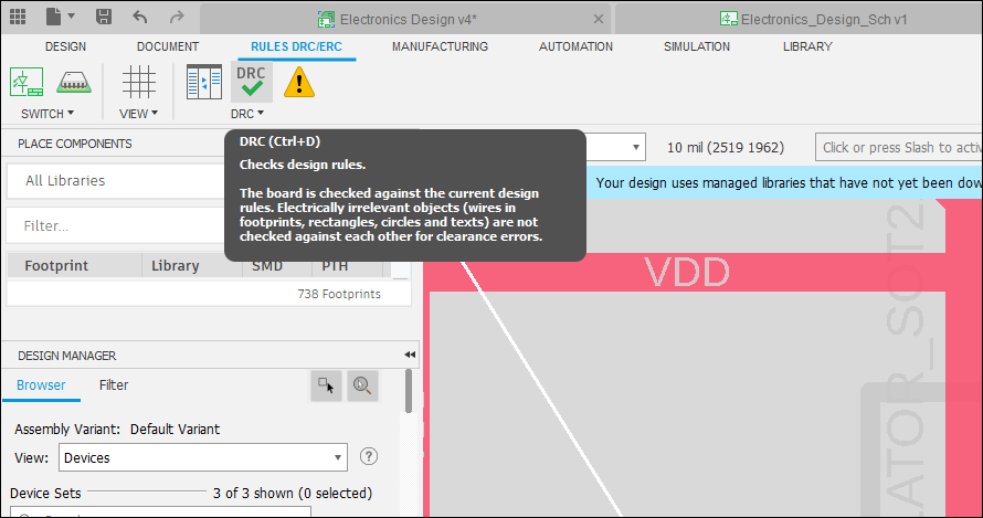
toolbox called DRC, to get there you should go to the upper bar, select the DRC
/ ERC tab, and click in the DRC button (or press Alt + F4).
There
you can set the different rules which will be followed as a preset when you
design, although they can be overrun if needed for your design. Due to this
possibility, you can make mistakes that will lead to certain design flaws
within your board: wires being too thin, small clearances that difficult the
wielding of components or wires being too close to the board limits.
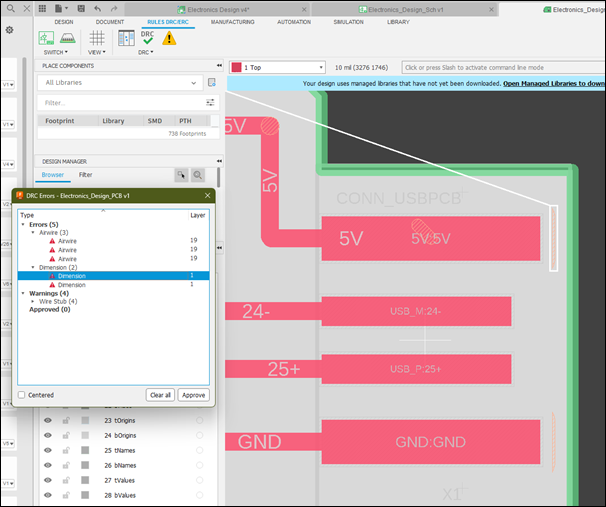
So,
if you want to know beforehand if you have made this mistakes, there is an
Error check button that will display the problems within your design, then you
can decide whether or not they are allowable.
For
example, in my design there were some design errors displayed when using this
feature, there were a couple of wires too close to the board limit, but once I
checked them out, they were the USB connector pads and it was part of the
design I needed, so I disregarded them.
Finally,
exporting them to png files that will be readable by
the Mods Program:
3rd step.
Electronics production
To send the milling and cutting files
to the machine we used a different method than the one used during the group
assignment. Now, the computer was directly sending the file to the machine from
mods, and we did not used the processor program. The parameters where the same
that we were using before.
Here are the parameters I used for
milling:
-
Tool Diameter: 0.0156 in
-
Cut depth: 0.004 in
-
Max depth: 0.004 in
-
Offset number: 6 (used this to create
a cleaner area to work with even though it needs more time to be done)
-
Speed: 2 mm/s
And these are
the parameters I used to cut:
-
Tool Diameter: 0.0625 in
-
Cut depth: 0.024 in
-
Max depth: 0.072 in (made in 3 steps)
-
Speed: 3 mm/s
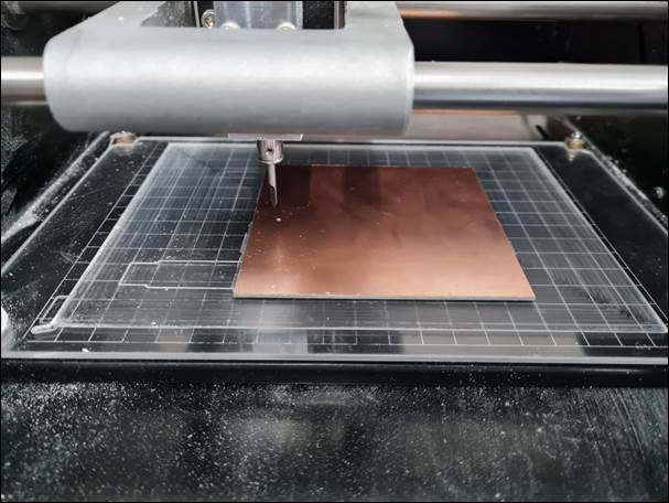
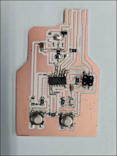
Finally, after a few tries, getting
the work done correctly. Next step is to fix the components and set up the
board for programming. This is how it looked like after fixing everything in
place.
4th step.
Programming
For this stage I had to create a programmer board used exclusively for
programming my different boards I was going to use for the different
assignments. This was also created from Adrian Torres SAMDINO
page, and programmed with EDBG as follows (Windows):
-
Download EDBG software to the PC in
any folder, it is in: https://github.com/ataradov/edbg
-
Download EDBG Free
Dap Bootloader file and save it in the EDBG folder.
-
Open Terminal.
-
Go to EDBG Folder.
-
Type the next command: <<
edbg-windows-r38.exe -b -t samd11 -epv -f
free_dap_d11c_mini.bin >>.
-
If everything is plugged in correctly
and working your board is now a free dap programmer.
This works to
only to create a programmer board. Next, I had to program my new board. For
that we need to download a bin file for a SAMD11C14A
from Mattairtech page. Save it to the EDGB Folder,
open Terminal and go to EDBG Folder. Type the following command: <<
edbg-windows-r38.exe -b -t samd11 -epv -f
sam_ba_SAMD11C14A.bin >>.
Now we should
download the Arduino IDE and change a few parameters to let it control our
board:
-
Open Arduino IDE.
-
Open Preferences
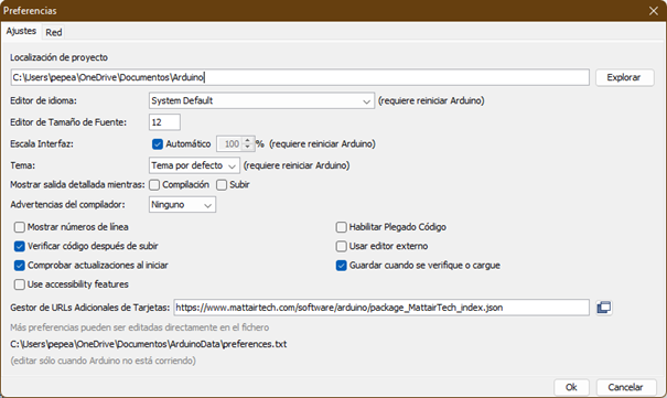
-
Open Additional Boards Manager URLs
and type: << https://www.mattairtech.com/software/arduino/package_MattairTech_index.json
>>
-
Go to Tools - Board Manager and install the Generic
D11 board Manager:
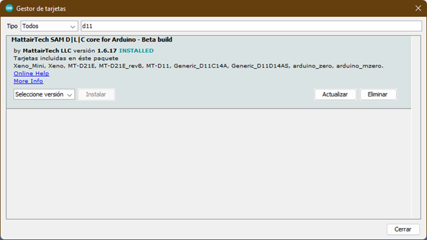
After this, you will be
able to use your board as an Arduino Board for programming purposes.
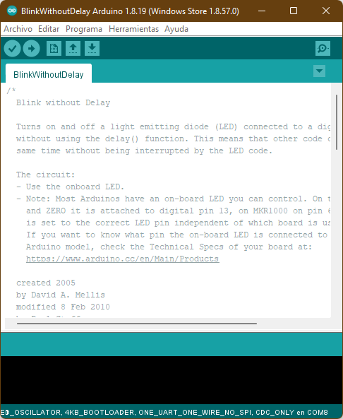
To test the board I
uploaded a << BlinkWithoutDelay >>
program that I found within the Arduino precharged
files.
Conclussions
This assignment importance was to
learn how to modify the existing schematics to take advantage of the work that
already has been done within the FabAcademy universe.
We must have an understanding of what do we need and how this components work
to be able to modify them.
Original
Files
1. Original
Files (f3z, brd, sch, png)
Nueval
Checklist
-
Linked to the group assignment page.
-
Documented what you have learned in
electronics design.
-
Explained problems and how you fixed
them.
-
Included original design files.
-
Included a hero shot of your board.
-
Loaded a program and tested if your
board works.
2022