Jose Alegria - Fab Academy
![]()
![]()
![]()
![]()
Electronics
Production
Assignment
wHAT iS THE ASSIGNMENT ABOUT?
Make an in-circuit programmer that
includes a microcontroller by milling and stuffing the PCB, test it to verify
that it works.
GROUP ASSIGNMENT:
What did I learn:
·
We had a few issues with the
characterization and tried different ways to link the files we were trying to
mill and cut and the machine. Once we solved them, our process was easier.
·
The different ways had different ways
to achieve the same parameters, you must have a correct comprehension of the
meaning of each of the settings and only then you will be able to use a machine
that works in a different environment.
·
The most important settings are
speed, tool diameter and cut depth.
1st Step.
Introduction to electronics
As we are going to make an electronic
board for the first time, we should get familiar with the names for the
different materials and equipment we are going to be using:
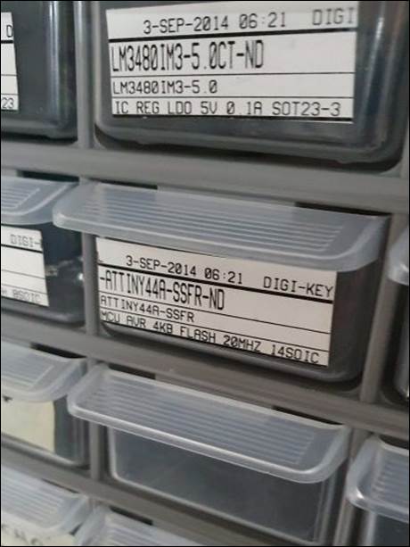
Materials:
-
Copper board: Here in Fablab Mexico City, we are using two kinds of copper
boards, both work similarly but are made of different
materials. The first one is a single sided glass epoxy board covered with a
copper sheet that is conductive, and the second one replaces the glass epoxy
with phenolic paper (also known as bakelite). We are
using them indistinctly and the main difference will be the resistance when
milling. We have various sizes, but the most common one is 4X4” (10 mm X 10
mm). If you need to mill a smaller size board, it is recommended to previously
cut the board to work with a smaller area (this is different from the cutting
we are going to do further ahead with the machine).
-
Welding: The basic material used to
get the electronic materials attached to the board, there is not too much to
worry about it.
-
Resistors: They limit the amount of
current going through the conductors, therefore protecting other components.
-
LED: We will be using them to signal
us if something is working or not, mostly they are optional. You must identify
the cathode because they will not work if installed incorrectly; usually in the
schematics it is marked with dots or thicker lines, within the LED it could be
marked with a green or black line.
-
Capacitor: They are used to store
energy and their measures are expressed in Farads (F).
-
Header: Pins used to plug the board
to any other component for programming or transmitting information.
Equipment
-
PCB Cutting and milling machines.
-
Welding equipment.
-
Voltimeter.
2nd Step. Getting
a design
To make an electronic board we have
two main paths to follow:
-
Find someone within the Fabacademy
universe who has made the same thing we want to do and use their board
schematics
-
Find someone who has made something
that kind of does what we have to do and make the
appropriate modifications to get it where we want.
Either way we
must get two or three images (we are using png files)
to get the following:
-
Traces
-
Holes drill
-
Outline
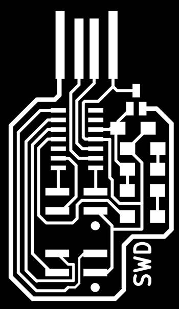
Here, we will
be using the following images to make our programmer board:
-
Outline:

-
Traces:
3rd step. Cutting
This step is, perhaps, the most
time-consuming of the entire process. We will mill and cut using our Roland
Modella MX-20 and the appropriate Mods Program to create a file from our png image and send it to the machine. For more information,
please refer to the group assignment page.
Here are the parameters I used for my
own board for milling:
-
Tool Diameter: 0.0156 in
-
Cut depth: 0.004 in
-
Max depth: 0.004 in
-
Offset number: 6 (used this to create
a cleaner area to work with even though it needs more time to be done)
-
Speed: 2 mm/s
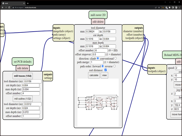
And these are
the parameters I used to cut:
-
Tool Diameter: 0.0625 in
-
Cut depth: 0.024 in
-
Max depth: 0.072 in (made in 3 steps)
-
Speed: 3 mm/s
4th step. welding
and fixing all the components
Welding was the most difficult task
to accomplish, that is because it requires a manual ability and to get some
practice before doing it well.
Here are some recommendations that we
followed during this process:
-
There are two ways to work, starting
with the microprocessor to have plenty of space to work with, or leaving it
towards the end because to avoid excessive heat to damage it. Either way will
work, I started with the microprocessor and had difficulties with the headers
(I have not found a perfect way to weld).
-
LEDs and Regulators have a correct
position, you have to be aware of where the cathode is
and work accordingly.
-
The other components are easier to fix
because there are not heat related risks or space related issues.
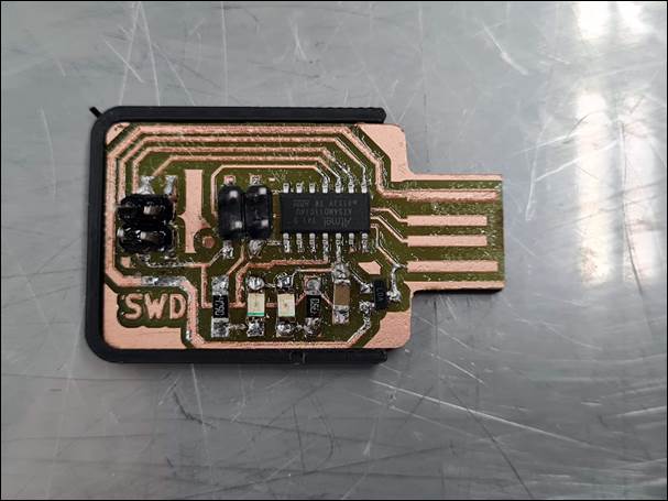
Once you finish
fixing all the components you should check for discontinuities with the voltimeter, that will help you find any mistakes done and
correct them before proceeding to board programming.
5th step.
Programming the device
For this stage I
had to create a programmer board used exclusively for programming my different
boards I was going to use for the different assignments. This was also created
from Adrian Torres SAMDINO
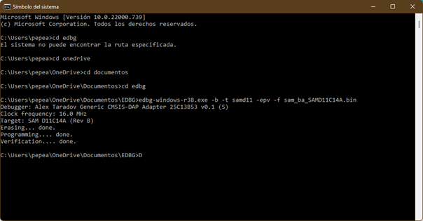
page, and programmed with EDBG as follows (Windows):
- Download EDBG
software to the PC in any folder, it is in: https://github.com/ataradov/edbg
- Download EDBG Free
Dap Bootloader file and save it in the EDBG folder.
- Open Terminal.
- Go to EDBG
Folder.
- Type the next
command: << edbg-windows-r38.exe -b -t samd11 -epv -f
free_dap_d11c_mini.bin >>.
- If everything
is plugged in correctly and working your board is now a free dap programmer.
This is a
picture of the SWD programmer being plugged to be programmed:
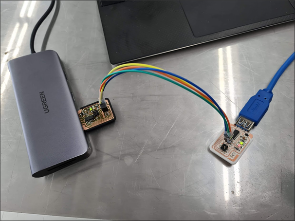
As
you can see, the best way to plug the connectors between the programmer and a
board is by signaling somehow where the GND pin is. The programmer board has
two sets of pins, one is designed to get the board programmed and a second one
to program different boards. For that part you should have the correct
bootloader file, for my board is the sam_ba_SAMD11C14A.bin file, which should
be stored in the same folder we are working on and then use the same command to
call it: << edbg-windows-r38.exe -b -t samd11 -epv
-f sam_ba_SAMD11C14A.bin >>.
Once the programmer is ready, you can
use it to program any other board:
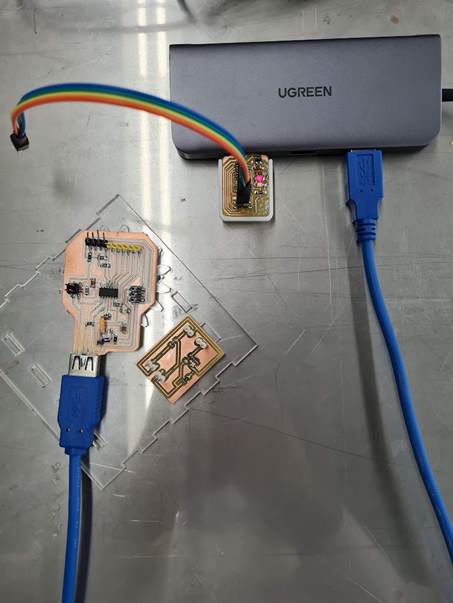
In
this video we can see how you have to plug the
connectors to program a new board:
Conclussions
This assignment importance was to get
used to what we were going to be doing for a few weeks. I got to learn the
different components and what are they for. And most important, the principles
and basics of electronic boards where I should get my design ready as soon as I
can, because there are too many mistakes I could make in the process, so if I
do not have enough time to repeat the processes, I am going to be having more
problems than I should, during the next weeks.
Nueval
Checklist
ü
Linked to the group assignment page.
ü
Documented how you made (mill, stuff,
solder) the board.
ü
Documented that your board is
functional.
ü
Explained any problems and how you
fixed them.
ü
Included a hero shot of your board.
2022