Electronics Design (WEEK 7)
Individual Assignment:
- Redraw an echo hello-world board,
add (at least) a button and LED (with current-limiting resistor) check the design rules, make it, and test it extra credit: simulate its operation
Group Assignment:
- use the test equipment in your lab to observe the operation of a microcontroller circuit board
IMPORTANT NOTE : ALL OF MY IMAGES ARE POP UP IMAGES , IF YOU HAVE ANY PROBLEM READINGS THOSE IMAGES , PLEASE CLICK ON THEM AND THEY WILL ENLARGE AUTOMATICALLY AND YOU CAN READ THEM EASILY
Individual Assignment:
For this week we were instructed to Redraw an
Hello echo-world board using PCB designing software
with clear instruction that it should have atleast
- * it should be programable it
* It should have 1 LED
* It should have button as well
Software i used to design the PCB
Autodesk EAGLE

EAGLE contains a schematic editor, for designing circuit diagrams. Schematics are stored in files with .SCH extension, parts are defined in device libraries with .LBR extension. Parts can be placed on many sheets
and connected together through ports.
The PCB layout editor stores board files with the extension .BRD. It allows back-annotation to the schematic and auto-routing to automatically connect traces based o n the connections defined in the schematic.
You can the download the original software by clickinh on this link and it will guide you to their official site from where you can easily download it
Getting started with software
STEP : 1
1. Once the software is succesfully installed you need to login first to your AUTODESK account
STEP : 2
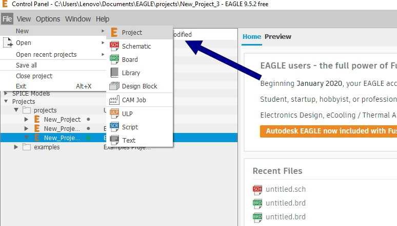
2. Then open the EAGLE and then click on 'FILE' option on the top right connor of the screen and then click on 'PROJECT' option
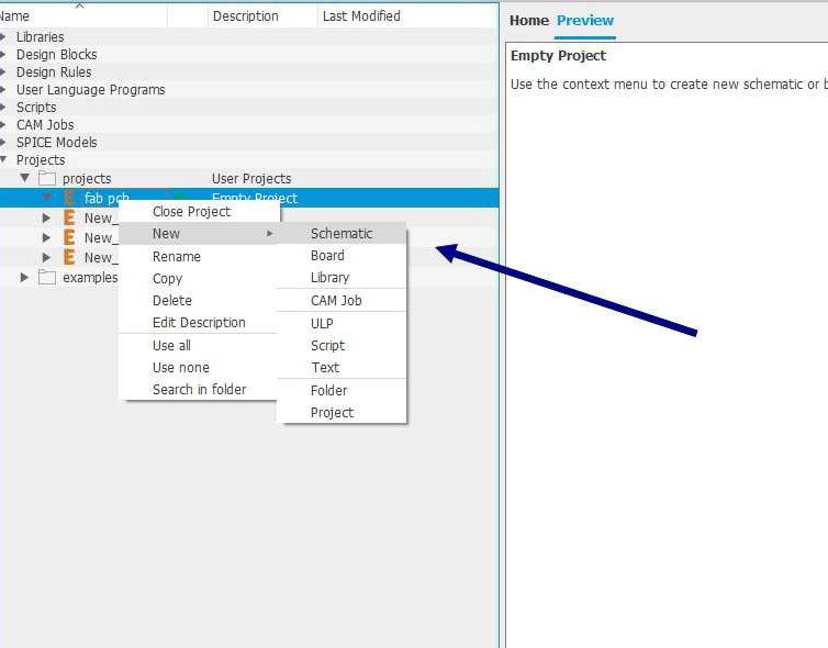
STEP : 3
3. Then Right click on the newest project which pop on the list of projects then select 'NEW' then select 'SCHEMATIC'
STEP : 4
4. before we can start working we are required download some libraries , so or that purpose please follow these steps
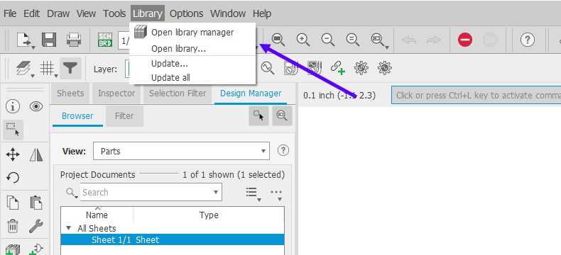
4.1 Click on the 'LIBRARY 'option situated on the top right corner and then select 'OPEN LIBRARY MANAGER'
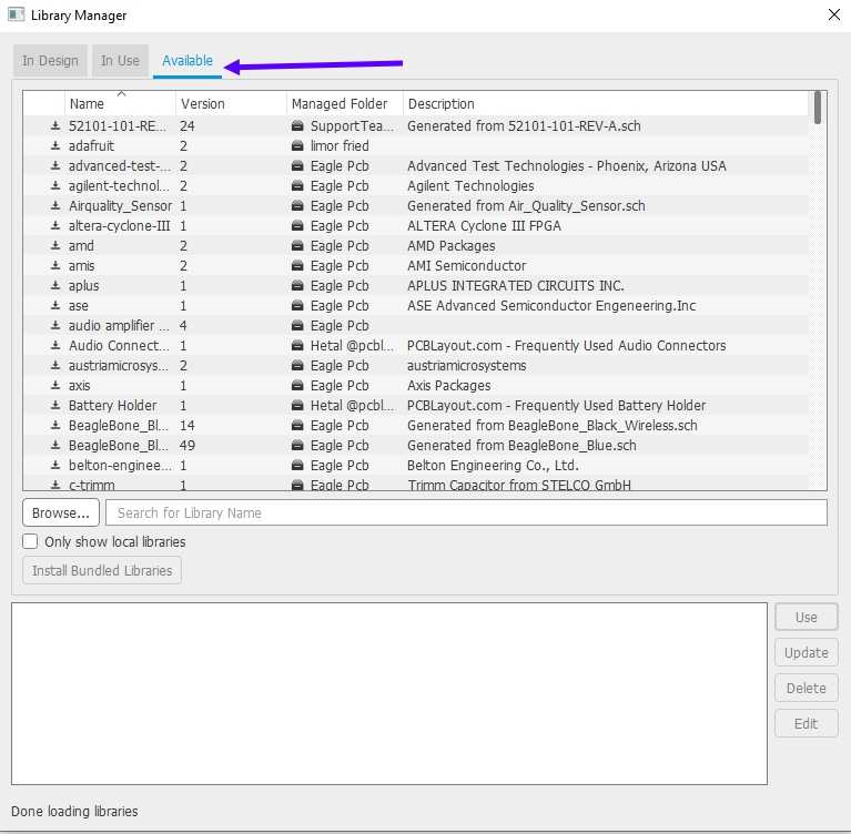
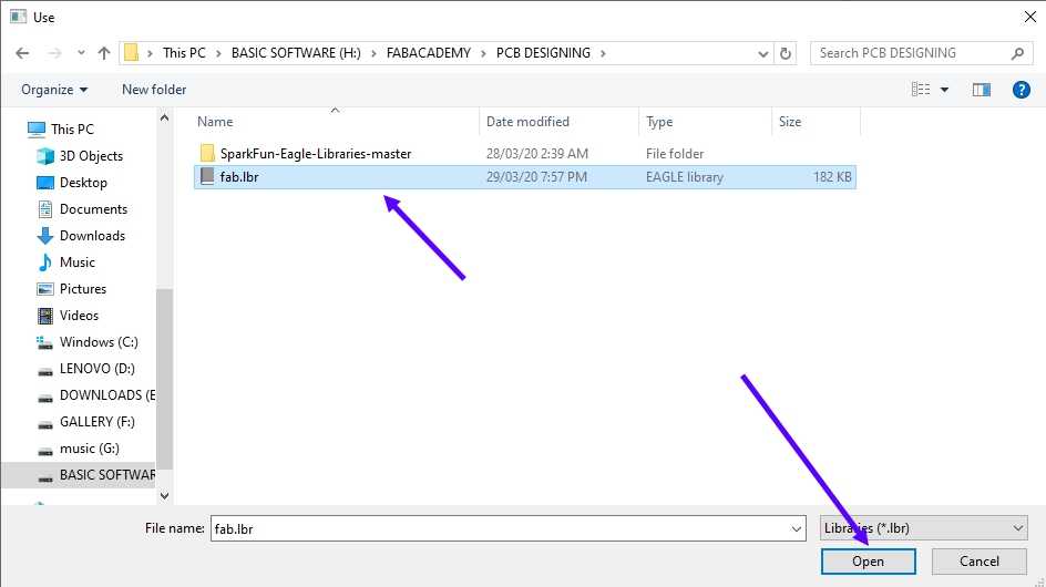
4.2 After that an small Selection box will be appeared on the screen , select the 'available' option and then on the 'BROWSE' option to add new libraries
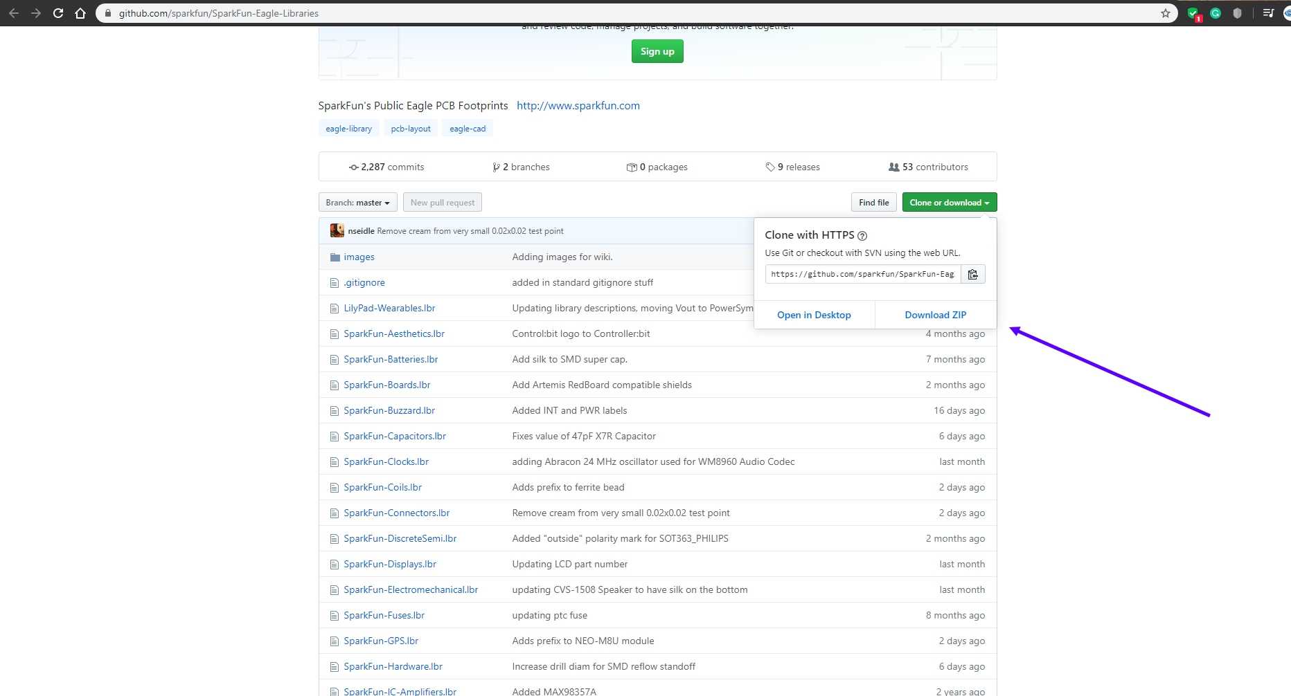
4.3 You can download the required library by clicking on this link and i am also listing one more library here you should also download in case there is any components missing in the above library
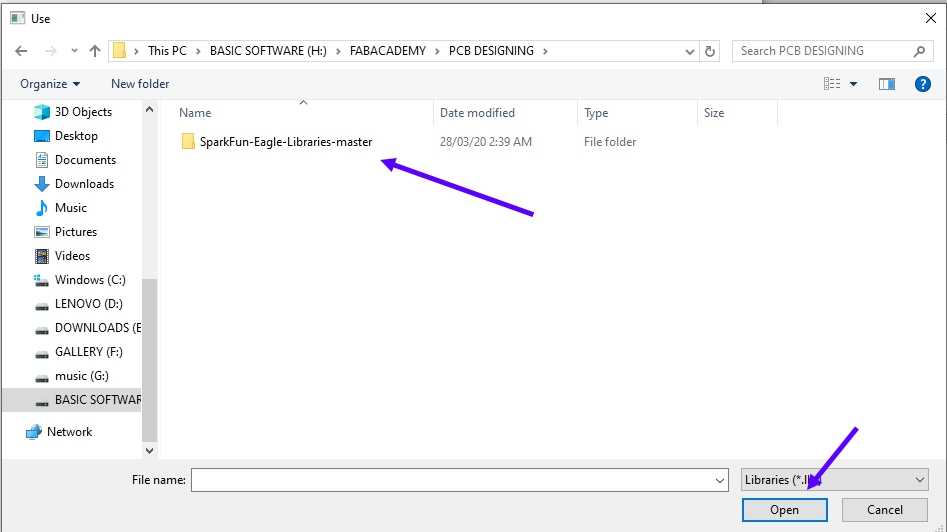
4.4 After you downloaded these library please add those to EAGLE 1 by 1
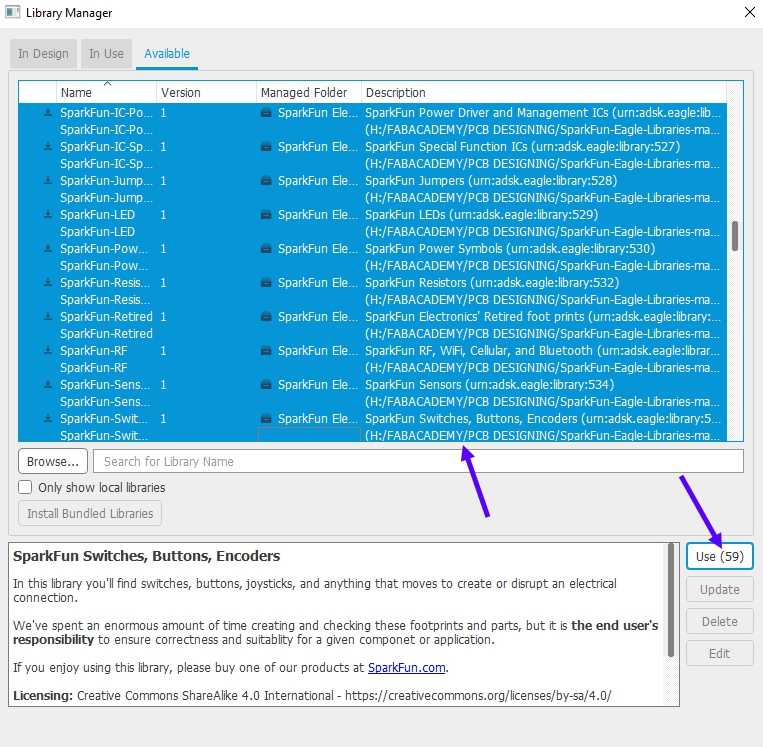
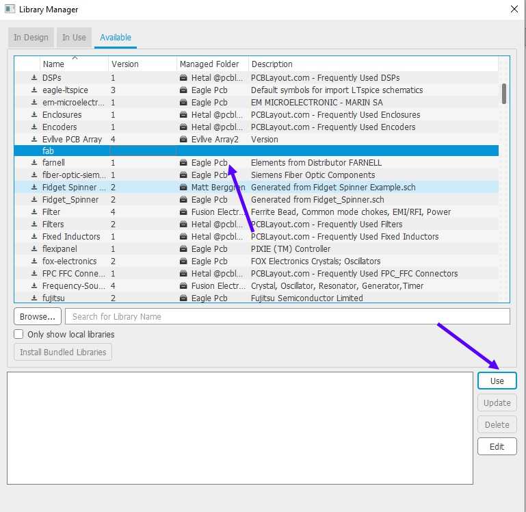
4.5 Select all the components listed in that library and then click on "USE" command and do same for both library
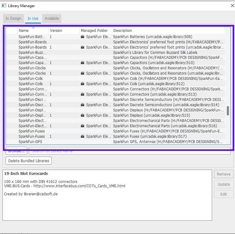
4.6 After that check that did those components are added or not
STEP : 5
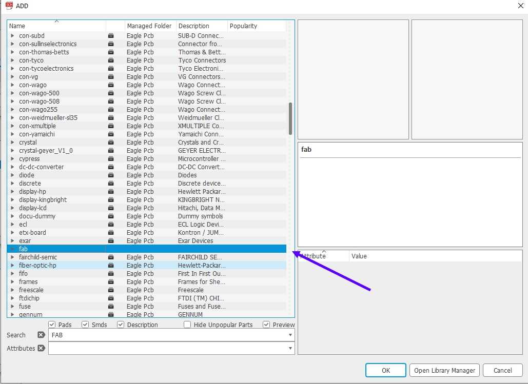
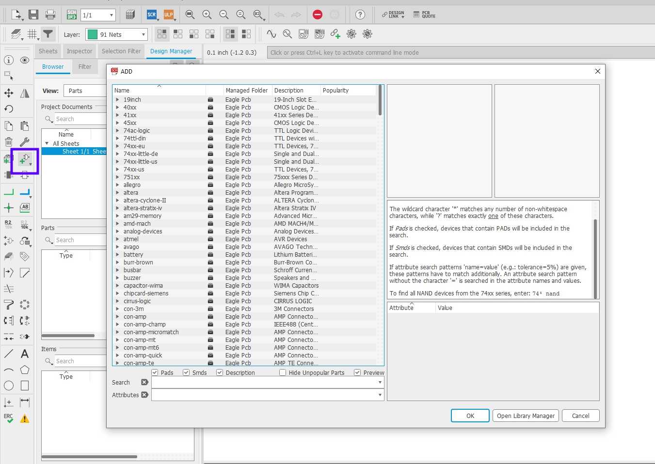
5. Now after all the libraries have been added we can start working on the PCB , so click on the add parts option given in the left tool menu
STEP : 6
6. But before you start Designing PCB you need to understand about the components you are going to used and this may vary Lab to lab , like some labs have 1 component nother lab that may or may not have that component
example : IC or the microchip which is the brain and most important component of any circuit can vary like my lab have These IC
-
* ATTINY 44
* ATTINY 45
* ATMEGA 16U
* ATMEGA 328P
please be free to click on any of the microcontroller to know about them more or you can also google them
So first you need to know what inventory your lab have and what it won't because it is meaningless to work on anything
best way to know about this is , go and catologue the things in lab
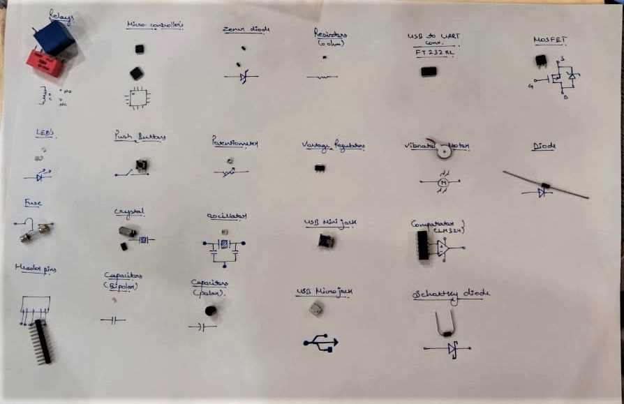
This image was taken by my teammate AFSHA RANA but this as usefull for all of us and this made us aware of differnt components we have in our lab
STEP : 7
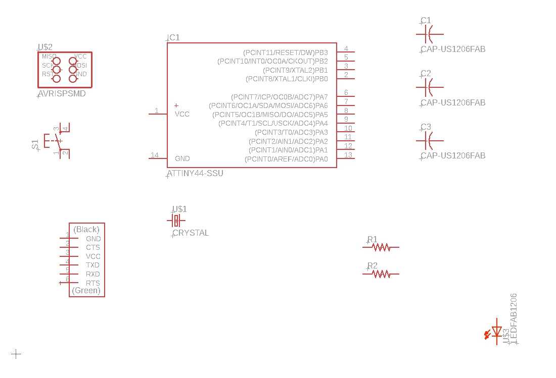
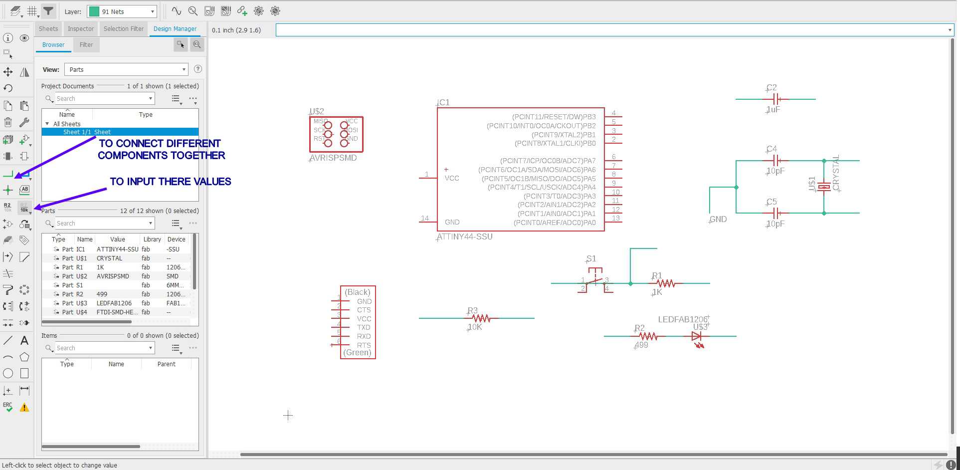
7. After you have choosed the desired IC or the available one , we need to start working on the schematic for the board , so pls dd all the required components from the libraries which we added previously , like i dd in this image
STEP : 8
8. I have also labelled the components so you can easily understand the names of components so you can take an reference
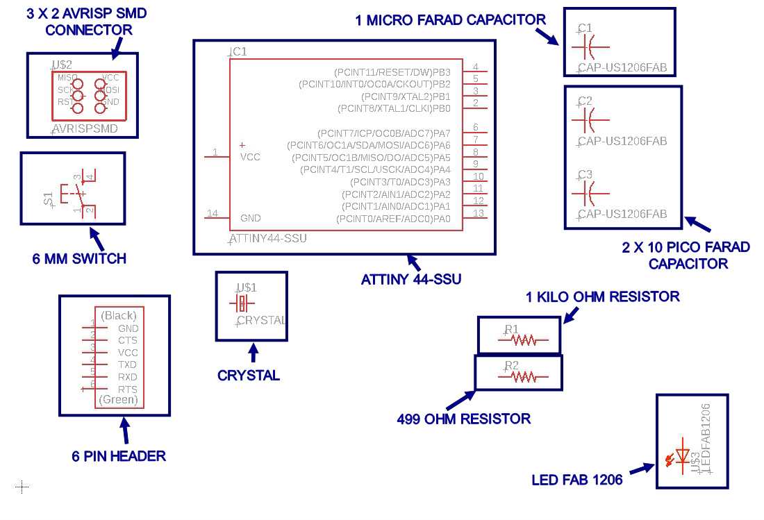
STEP : 9
9. After all the componentsare selected you need to give the values and you can do that using the tools i have mention in the above images
STEP : 10
11. Now we need to make connections btw different componenets so we can form an working circuit btw them and for this purpose there are 2 ways
1 Connecting them Manually using 'Net' tool using which have mention in above image
This is how you can connect them Manually
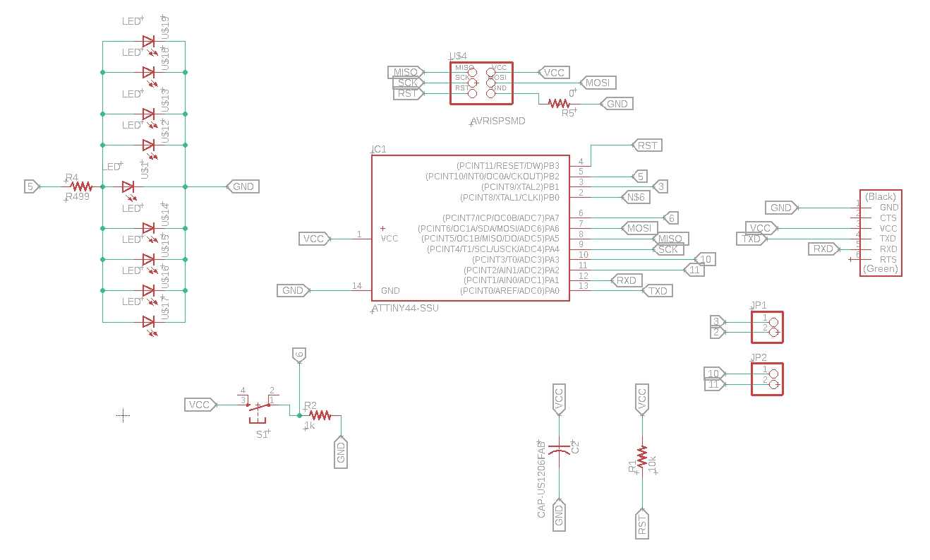
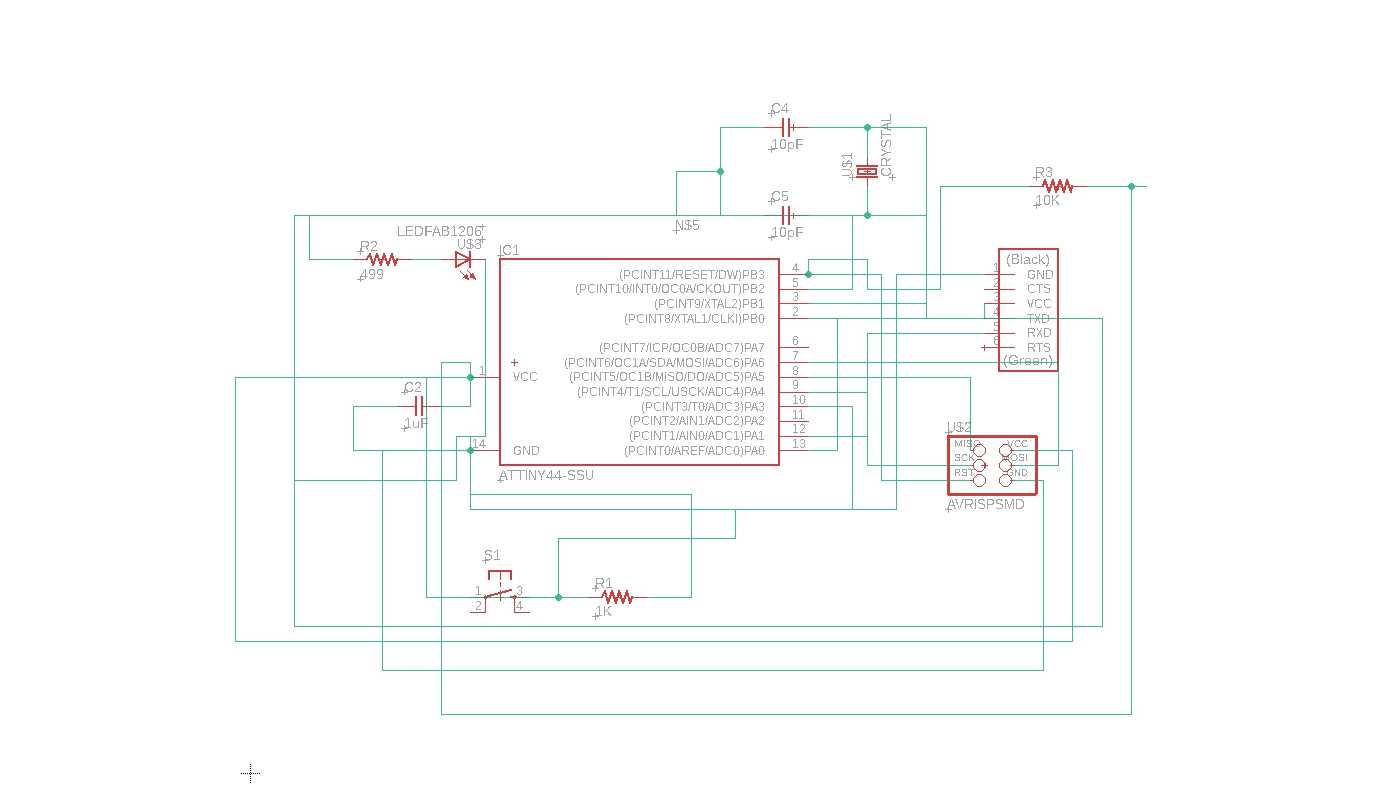
Second way is to connect them using "LABEL" tool ,you can have a look from the above design (Personal note: both the images are of 2 different pcb)
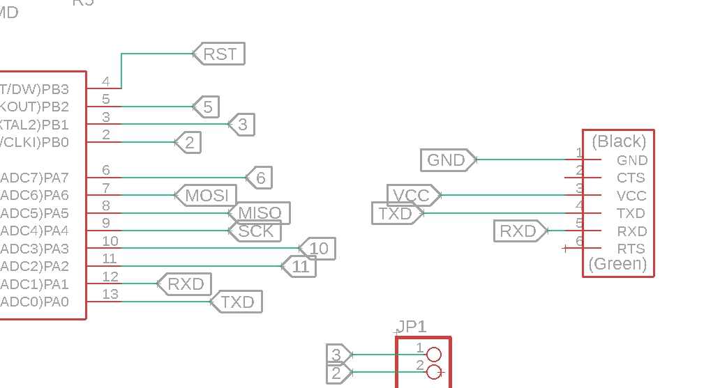
Through this image you can easily see this that both parts are easily connected by labels and there is no need of NET / lines to connect each other
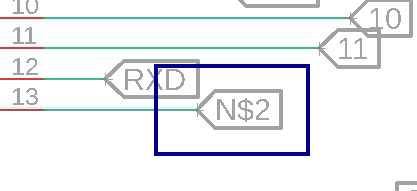
The above image represent an label
I have created an video showing how to correctly use a label so if you want to know how to use it please look to this video
PERSONAL NOTE : Well i like "NET" tool more as compare to "LABEL" tool because it was easy for me to trace back the connection rather than finding the position of correspondant label , but its all on the
                                                    user as both my teammate prefer "LABEL" for designing their PCB
STEP : 11
Check for ELECTRICAL RULE CHECK (ERC)
If this is your first time designing a schematic then the term Electrical Rule Check might be a bit new. This is a handy little tool that you’ll always want to keep in your engineering toolbox, as it helps to point out common errors in your schematic. An ERC will check for the following issues:
* Are all of your nets properly connected and labeled on your schematic?
* Do you have any conflicting outputs/inputs on your schematic?
* Are there any open or overlapping pins and ports on your schematic?
You can think of an ERC as a second pair of eyes; it will always be there to help you find the missing details that you may have overlooked! Of course, an ERC is not meant to be a replacement for reviewing your schematic manually, so don’t rely on it as your first level of defense.
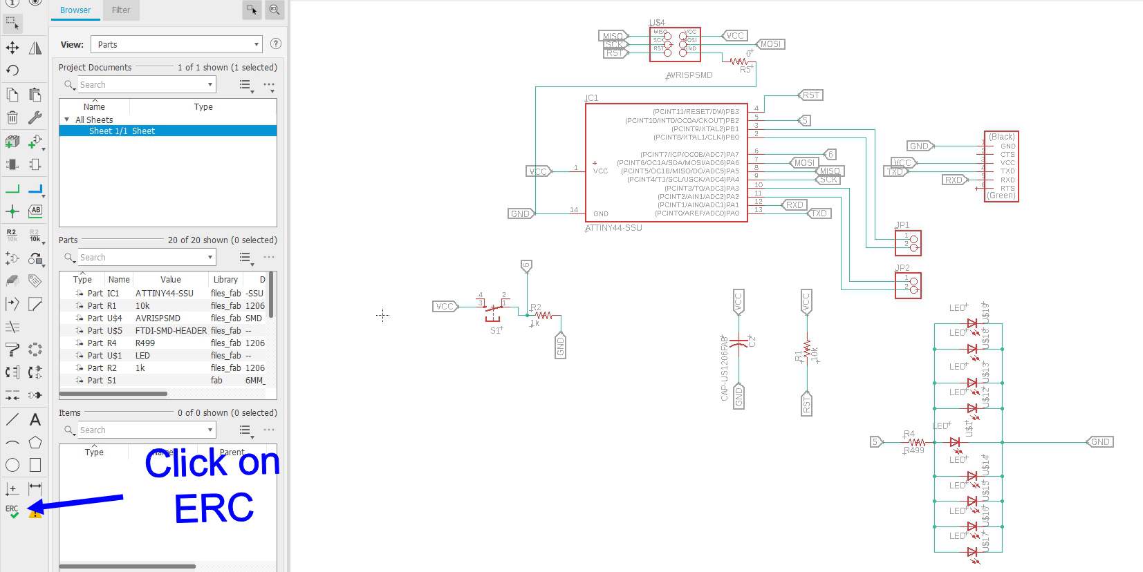
For checking ERC please click on the ERC option , as i have mentioned in the image
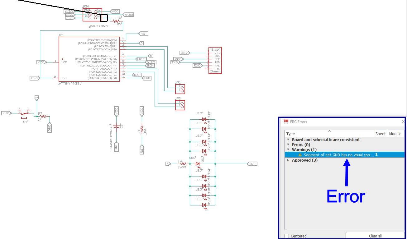
Once you click on this option a menu will be pop up and if your design have any problem it will be showed in this menu and clicking on the problem system will automatically guide you to problem and ask you to correct hat problem before moving ahead , it is really important that you resolve hta problem before moving to converting board into schematic.
STEP : 12
Upto this point you have completed 50% of your PCB and the Schematic part is about to finish and now you have to start working on the actual board
Please go through this video and you can learn how to convert your SCHEMATIC into board
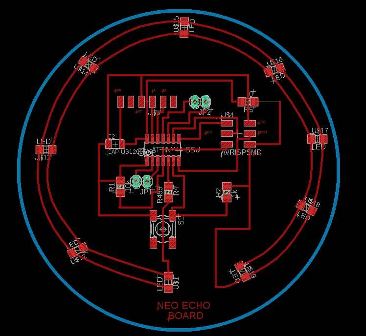
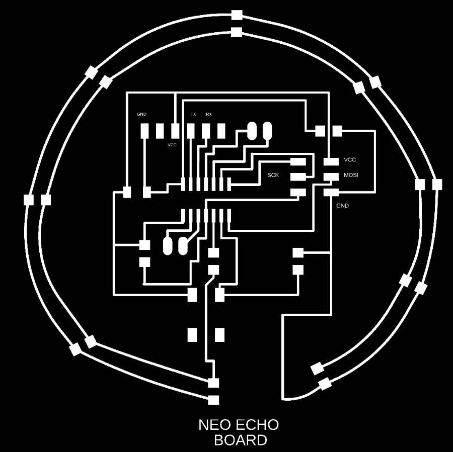
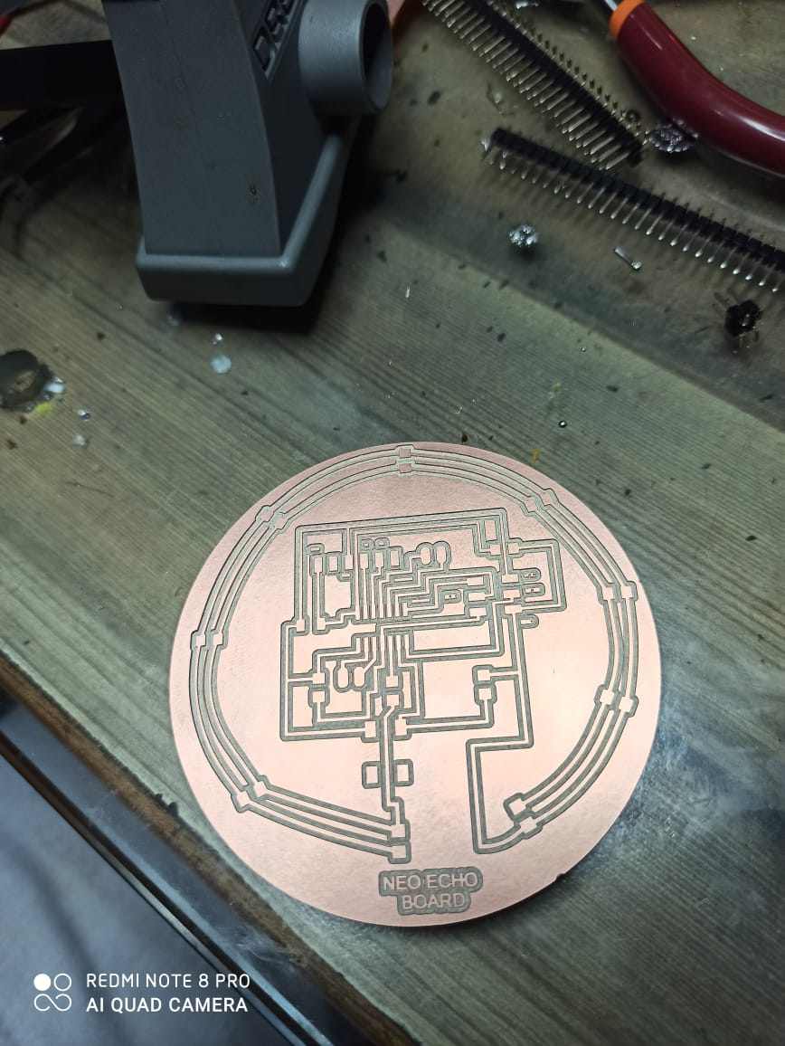
This is an fully ROUTED/completed board and i have named this pcb as "NEO EHO BOARD" because i realy love NEO PIXEL LED and speacily those LED rings , thats why i made it in the same image of those ring LED
Neo echo Schematic and board
STEP :13
Checking for DEDIGN RULE CHECK (DRC) error's
This stage is all validating your work through the use of a Design Rule Check (DRC). We will then add some much-needed copper pours. Once that’s complete, we can then move onto putting some polish on your board layout with the use of silkscreen text. Once those challenges are accomplished, it’s time to get that design of yours manufactured! You’ve come so far, let’s wrap up your PCB design once and for all.
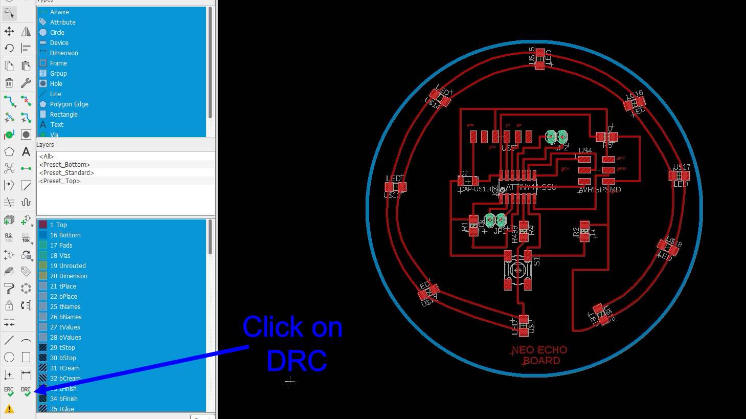
Like ERC , DRC is also very important before we can move to cutting Pcb , this step validate what we we have made or routed , it is correctly made , so for that pls click on the option given in left tool bar
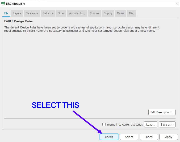
Once this option is opened click on the Check option so you can check that what we previously given
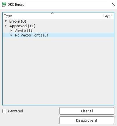
You require to temove all the air wire's and overlapping , plus the error DRC will show you before you can move to cut this pcb
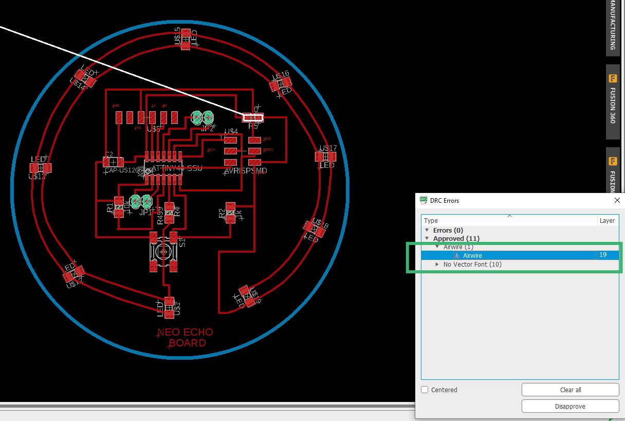
As you can see i have an air wire in my design , which was appeared because i required to add an 0 ohm resistor as there was an air wire in the circuit , so to eiminate that i required to do so , but DRC will recognise it as a failure and will ask me to remove that wire , but it wont effect the circuite as it is 0 ohm , so you can ignore these type of Air wire
STEP : 13
Now you need to convert you PCB into PNG image so you can generate G-code and M-CODE for your milling machine
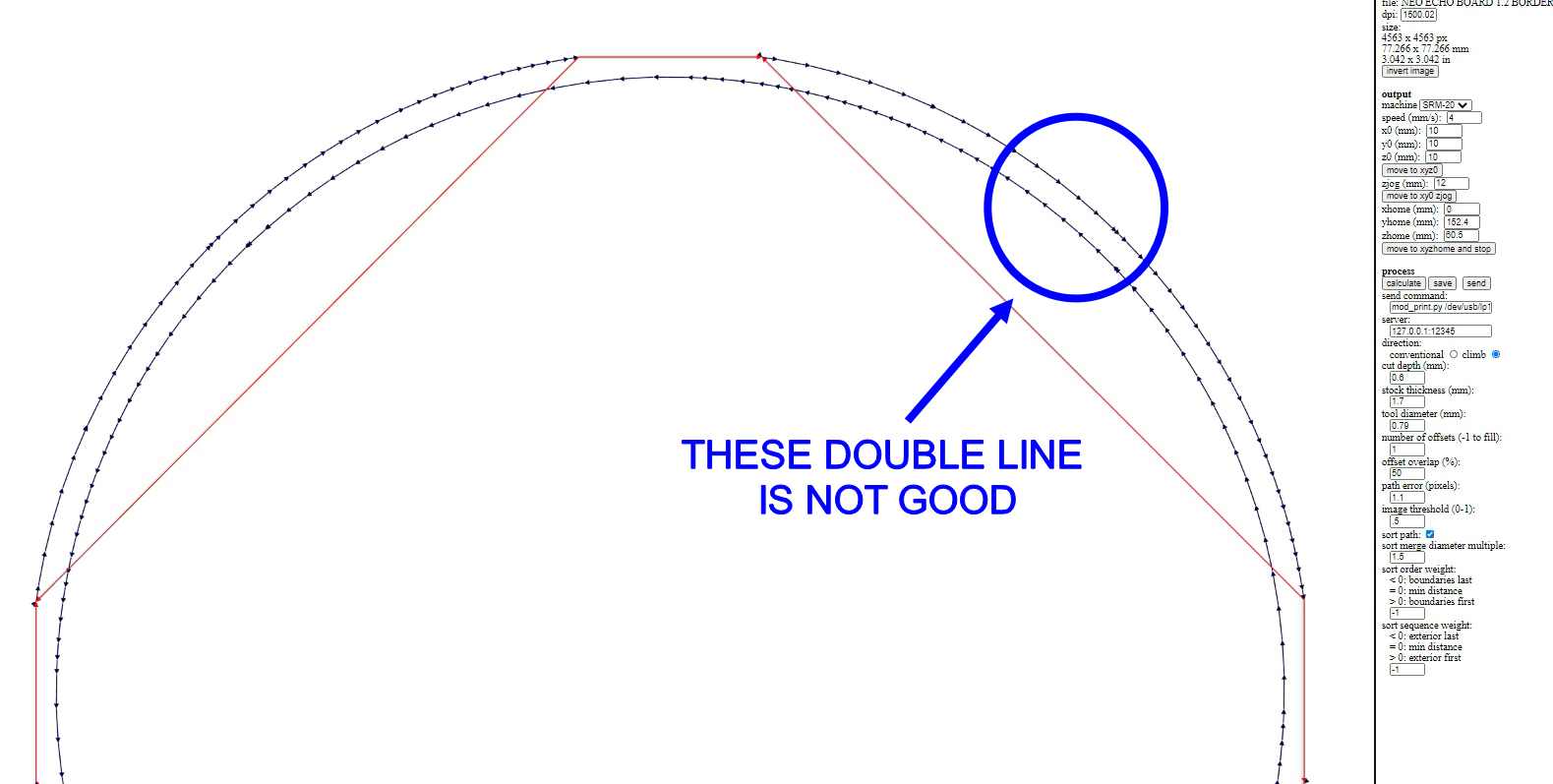
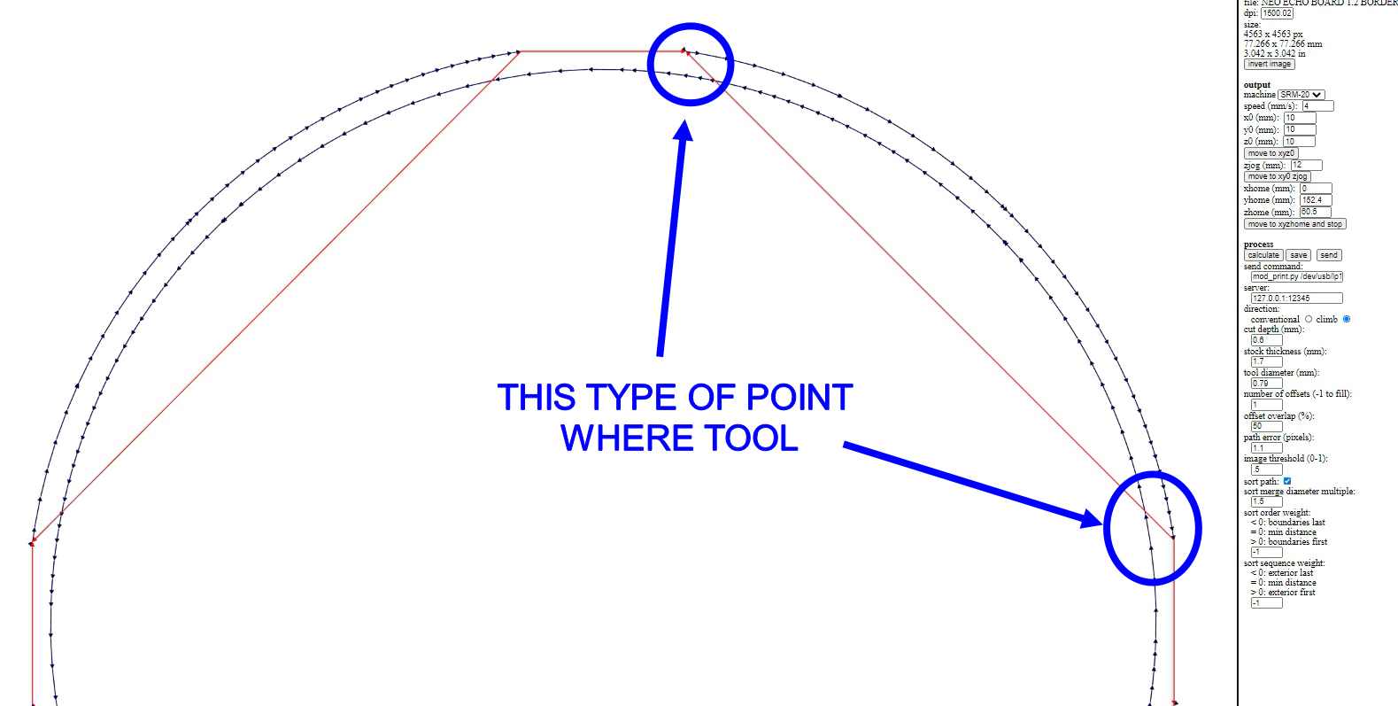
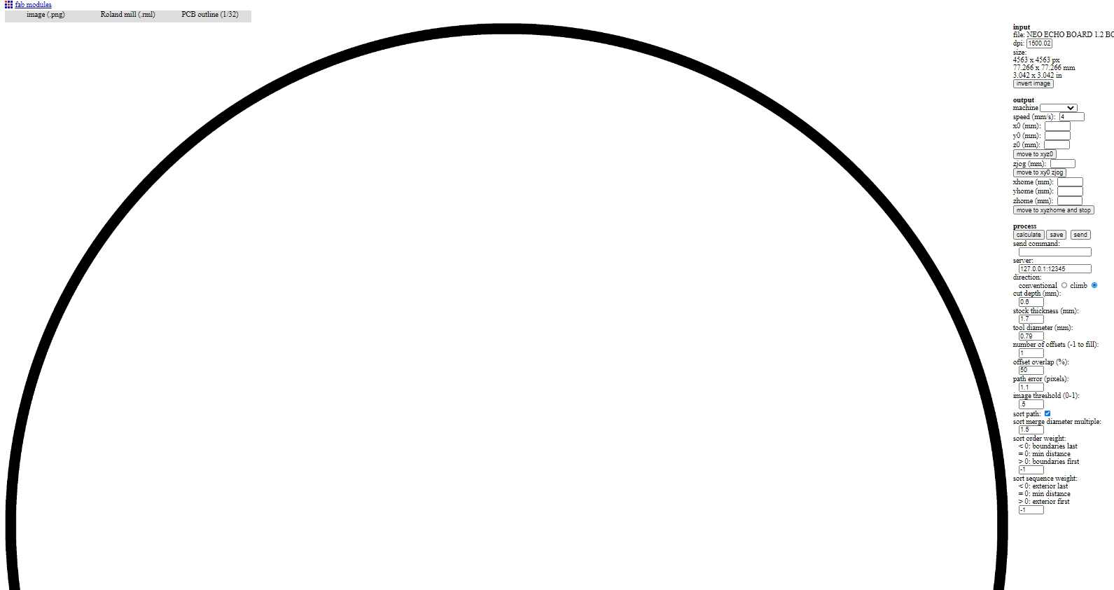
This is an PNG image for my PCB tracks which is needed to be cut using 1/64 inch end mill or in our case an V-BIT (because all the 1/64 inch end mill were broken so we neede to use V- bit)

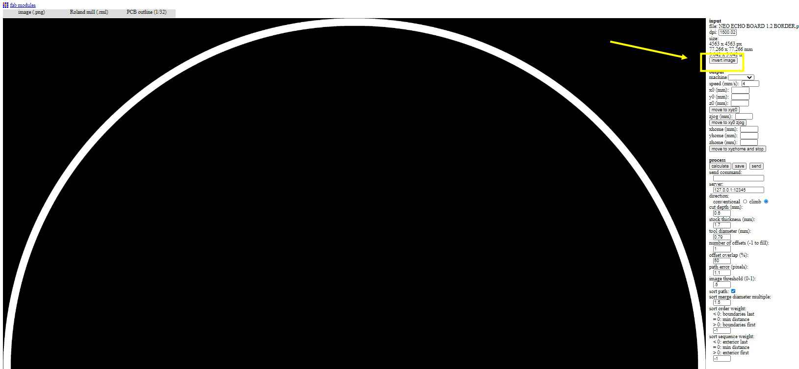
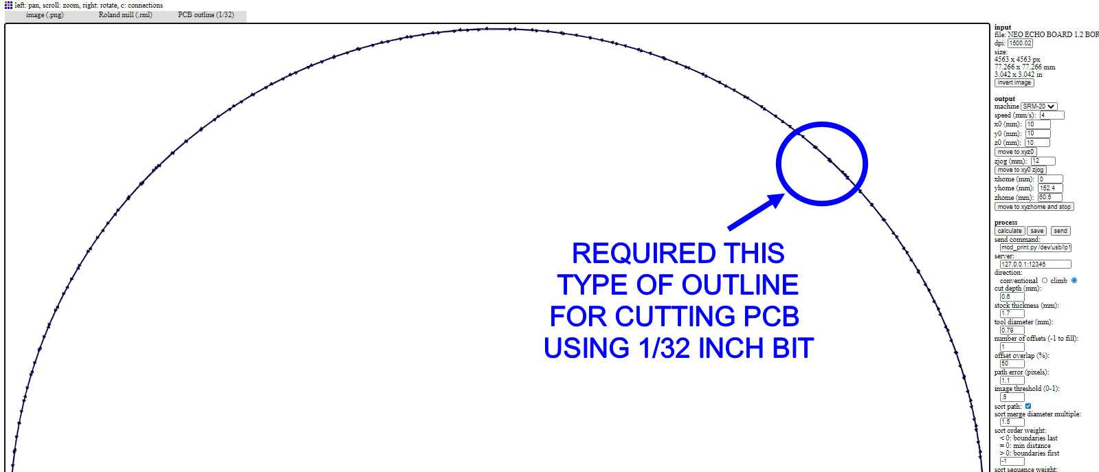
Similarly this PNG image is for my PCB boundary which is needed to be cut using 1/32 end mill
I have made this video explaining how you can convert your PCB in PNG image things to remember doing that
I am Also AddingPNG files for my PCB if would like to download it in any case
Neo echo Board PNG FilesSTEP : 14
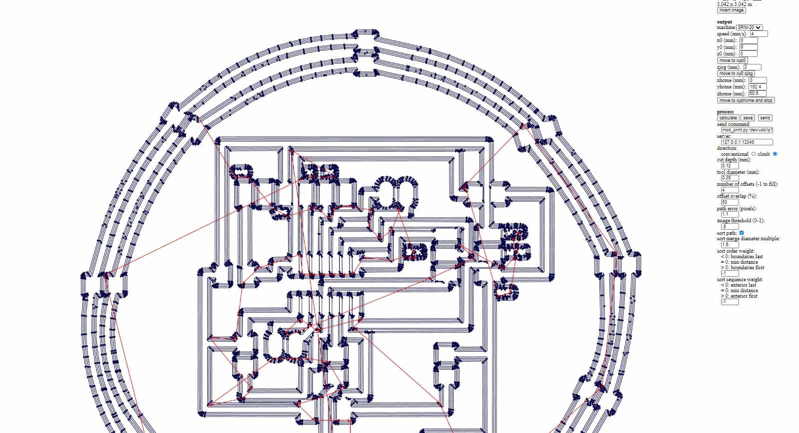
Now we nned to generate G-code and M-CODE , for that purpose I used FAB MODULE ,You can easily easily go on it by clicking this link
and if you want to know more about it you can easily go on my page
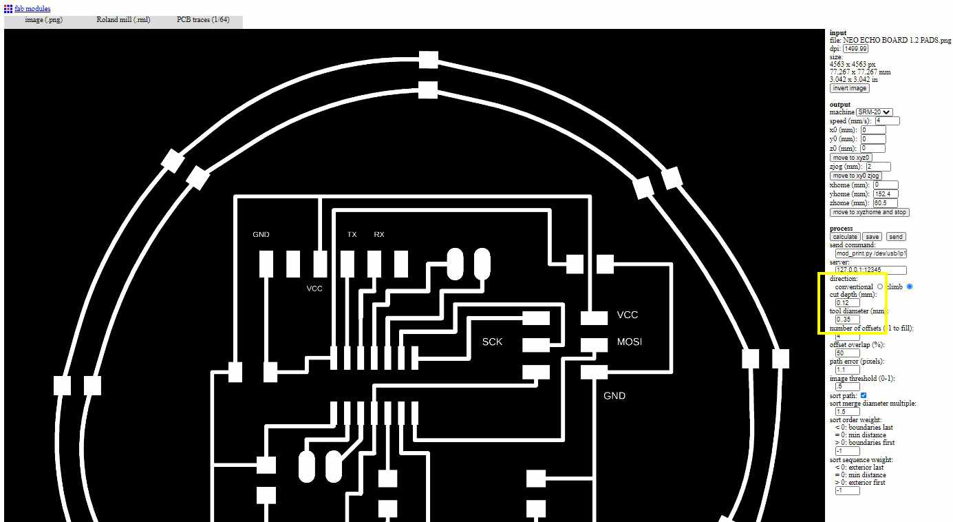
First converting PNG image for Pads
IMPORTANT NOTE : Here we are using an "V-BIT" end mill not 1/64 inch bit so we require to change some cutt settings like:
- 1. Increase "CUTTING DEPTH" from 0.1mm to 0.12mm
2. Decrease "TOOL DIAMETER" from 0.4mm to 0.35mm
Remember : Once you click on "CALCULATE" , you need to wait for FAB MODULE to give you all 4 offset line you require or whatever number of offset you have given , not before that because in fab module it takes time to give all the offset , it gives 1 by 1 and sometimes due to internet issuse it dont give all ofset so try again unil you get required offset, so please look closely before saving it
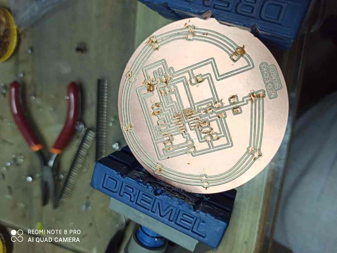
This is a high speed timelapse video of milling of my PCB
This is how it looks after milling is completed
Now we require to start soldering it , so first i applied soldering paste on all the points where my components are going to solder
Doing this proccess in first save lots of time and effort so i recommend this to every one
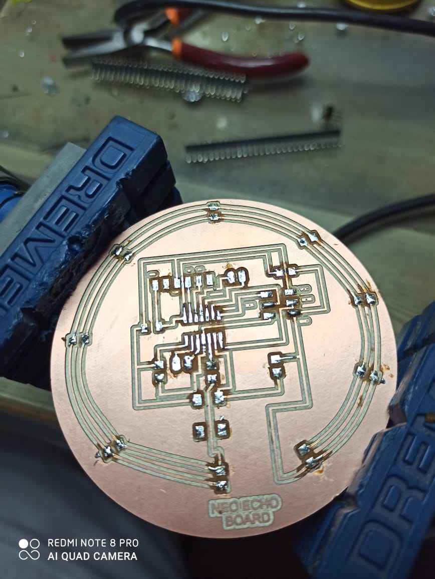
Ater that i aplied solder on all of the points where components are going to solder , you just need to apply very little amount of solder( i mean there should not be Lumb of solder on the pad it should be almost
flat)
doing this step in advance will really help you because it will provide you ease during soldering of SMD components
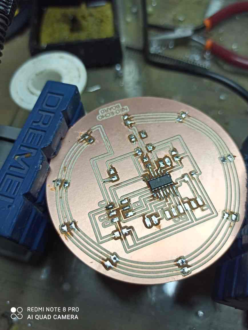
Always remember to solder the microcontroller/IC first because it is the most hard and trickiest of all and there is always an chance that you will shot 2 or more pins together which result in destruction of that chip when power supply is applied
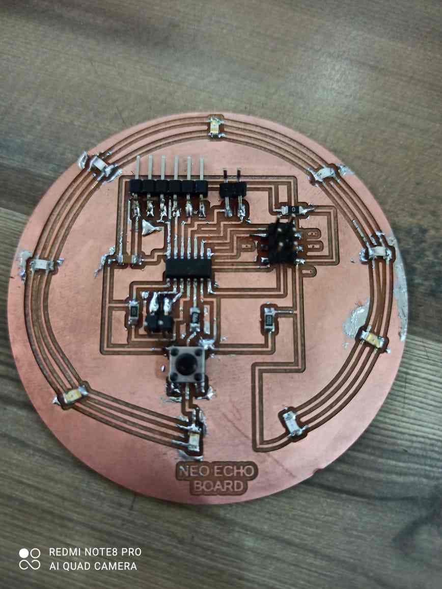
This is the fully soldered PCB
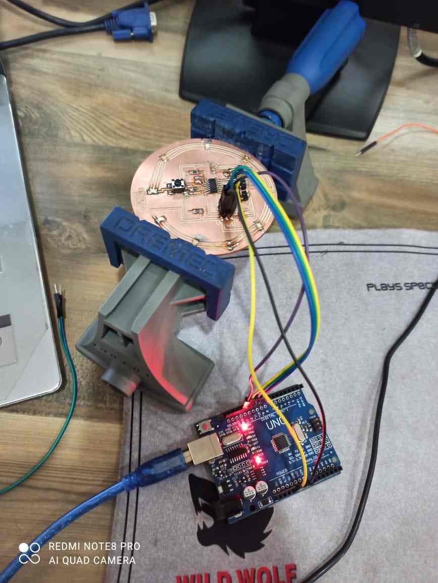
Now i have connected the pcb to an arduino to program it , if you want to know how i program it please click on this link , it will guide to my Embedde programming page , from where you can earn how you can program this pcb
This is the code for arduino
const int buttonPin = 6;     // the number of the pushbutton pin
const int ledPin =  5;      // the number of the LED pin

// variables will change:
int buttonState = 0;         // variable for reading the pushbutton status

 void setup() {
// initialize the LED pin as an output:
 pinMode(ledPin, OUTPUT);
   // initialize the pushbutton pin as an input:
 pinMode(buttonPin, INPUT);
  }
  void loop() {
// read the state of the pushbutton value:
buttonState = digitalRead(buttonPin);

// check if the pushbutton is pressed. If it is, the buttonState is HIGH:
if (buttonState == HIGH) {
// turn LED on:
 digitalWrite(ledPin, HIGH);
 } else {
// turn LED off:
 digitalWrite(ledPin, LOW);
}
 }
you can use this code by just clicking and copying it
Group Assignment:
This week assignment was to use the test equipment in your lab to observe the operation of a microcontroller circuit board
Lab Test Equipments
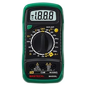
1.Multimeter
A Multimeter is basically a Paramter measuring tool, which can measure a wide range of parameters, Principally : Voltage (AC/DC), Resistance, Capacitance, Conductivity etc. Its the most common diagnostic tool technicians have, through multimeter debugging comes handy.
2. Variable D.C power supply
In our lab we have Scientific Unitec PS-305 (0-30V 5Amps) Power Supply .We used to give 5 volt-12 Volt power supply to our boards.
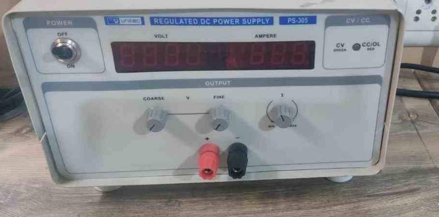
Key Features
1. Input Voltage Range 230 Vac
2. Brand UNITEC
3. Part Number PS30
4. Ripple Voltage 0.1mv
5. Output Voltage 30 Volt
6. Mounting Type Benc Type
7. Input Voltage 230vac
8. Maximum Input Voltage 240
9. Output Current 5amp
10. Design Compact
11. Maximum Operating Temperature 55
12. Display Type Digital DC OUTPUT : 0-30Volt DC CURRENT : 0-5Amp AC INPUT : 185 - 240 Volt AC
3. Digital Oscilloscope
One needs to understand the circuits on signal level, which multimeters fails to do. In this case Oscilloscopes is the answer. A digital oscilloscope measures the signal, and then converts that measurement into a digital format using an ADC converter, after which the data measured is depicted as a digital waveform representation. From this representation various paramters can be evaluated. In our lab we got Scientific TEKTRONIX TBS 1062 Oscilloscopes.
While working with electronics, for debugging and testing behavior, we need to understand the circuits on signal level, which multimeters fails to do. In this case Oscilloscopes come in picture. A digital oscilloscope measures the signal, and then converts that measurement into a digital format using an ADC converter, after which the data measured is depicted as a digital waveform representation. From this representation various paramters can be evaluated.
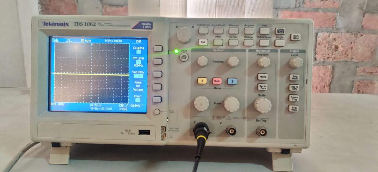
Key Features
1. 16 automated measurements, and FFT analysis for simplified waveform analysis
2. Built-in waveform limit testing
3. Automated, extended data logging feature
4. Autoset and signal auto-ranging
5. Built-in context-sensitive help
6. Probe check wizard
7. 5.7 in. (144 mm) Active TFT Color Display
8. Multiple-language user interface
9. Small footprint and lightweight - Only 4.9 in. (124 mm) deep and 4.4 lb. (2 kg)
Measuring Digital Signal:
We uploaded Blink code on the UNO board and we observed the pulse signal.Above are the results for the same.
Measuring Analog Signal::
We measured the analog signal by connecting both the probe of oscilloscope to Gnd and Vcc pin of dc motor and rotated the shaft manually