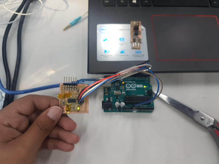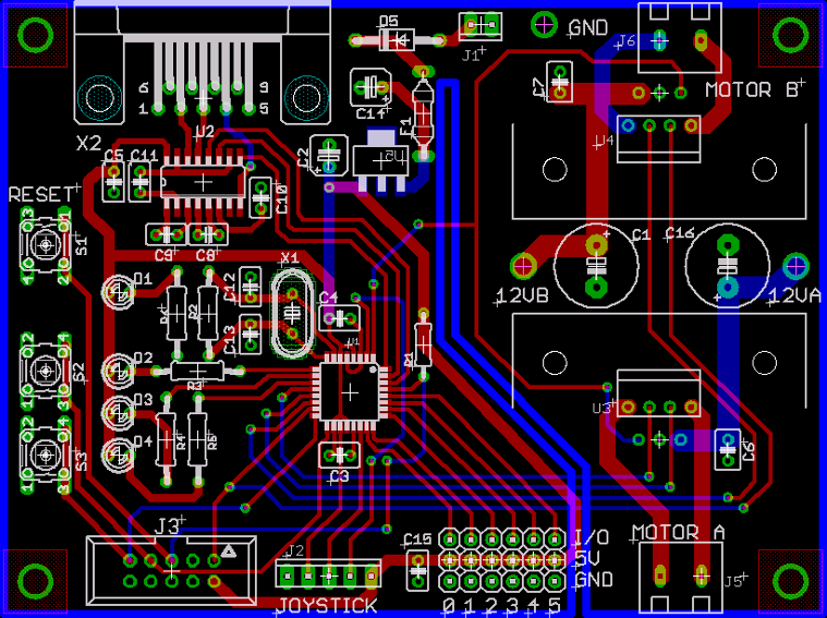
Electronics Design: learn how to design a PCB
This week of Fab Academy we have been introduced to electronics design using EAGLE. EAGLE is a scriptable electronic design automation application with schematic capture, printed circuit board layout, auto-router and computer-aided manufacturing features. One main and big advantage about eagle is that it is hooked up with different libraries which gave you the chance to basically design or modify any PCB you want.
The Component Library
In this assignment the first thing we had to do is downloading the component library which has all the component that we are going to use during this assignment. In general Eagle has different libraries that are already built in like (resistors, capacitors, and inductors), however, durin this assignment we had to download the fab library, which is a library created by Fab Academy and it has the special components that cannot be found in any other built in libraries in Eagle.
So the first thing first, to download the library I went to the tutorial provided from Fab Academy for this week lecture which is electronics design, and found the GitHub link provided for this library and downloaded the Zip file for it.
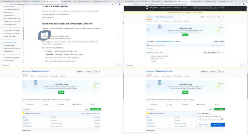
Then after downloading the library I should add it to EAGLE libraries to be able to access its components and use it in designing the "Hello" board assigned for this week. To do so I followed the follwoing steps; Eagle - New project - New Schematic - Library tab - Library manager, In the library manager I brows the library I downloaded which called fab, and then directly after adding the library it appered in the library list.
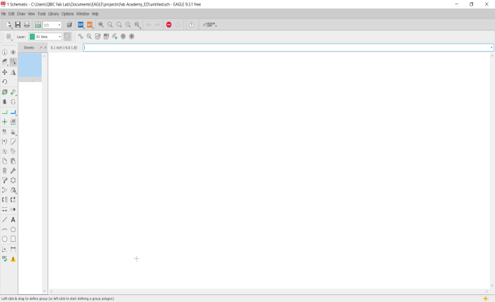

And by this I was successfully able to download and access the library to start designing the schematic of my PCB board.
Schematic Design
After adding the library required to EAGLE it is now the time to start desiging the circuit required for this assignment. For this assignment we are suppose to re-create the "Hello" board in EAGLE, and to do so first we should design the board in EAGLE's schematic.
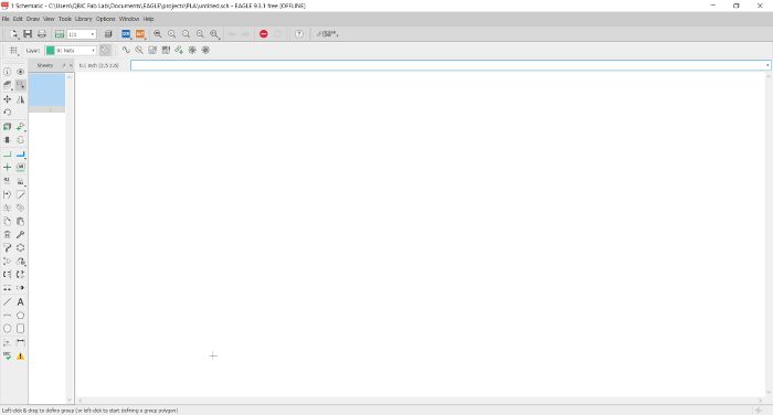
Basically schematic represent the electronics circuit drawings. The interface uses symbols to represent real-world electronics components. So to start building our circuit in the schematic we should first add all the electronics componenets in the schenatic interface. To add components we should go for the "Add Part" symbol.
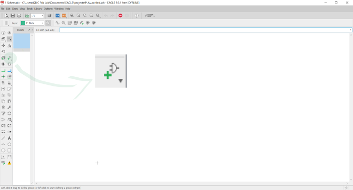
Then from the "Add Part" button we sholud look for the fab library to a start add all the required components from their to our schematic. The components required for this circuit are: 6-pin programing header, microcontroller, FTDI header, 20MHz resonator, resistors, button, ground, VCC, connect pin 10, LED, and capacitor.

After adding all the electronics component required now we should connect our circuit board together. Thers are two ways to connect the components together; one is by connecting them using wire or net, which is the common and direct way to do it. The other way is to name the nets or wirs attached to components that need to be connected by naming them with the same name. For me I did both connections, in some part of the schematic I used normal wiring technique to connect my circuit together, and in other parts I named the wire with the part that is connected to it.
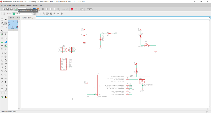
And by this I was successfully able to finish my schematic and now the next thing to do is generating the board and start routring the traces to form a neat connections.
Generate Board
To start generating the board we should shift from shcematic interface to board interface, and to do so we click on the follwoing button:
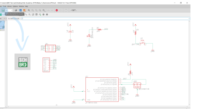
After shifting to the board interface the following panel will open with board layout, electronics componenets, and the traces or the connection between the components. After generating the board, the next thing to do is to rearrange the components in a way that you can find a good way to connect them without causing any kind of crossing that would short out your circuit.

To start forming the traces of our circuit board, we are going to use most of these tools:

Usign these tools we can strat routering our traces to form the final PCB board that we are going to use for milling. When routring the traces you should be carefull not cross any trace, or put traces closer to each other to avoid any short circuit while milling the PCB board.
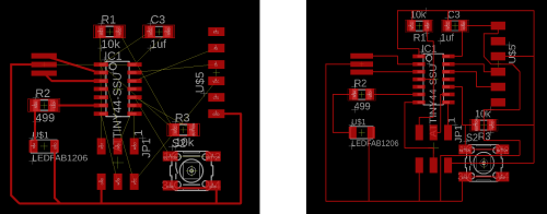
After finishing with connecting the traces together, it is now important to check the connections using the Design Rules Check (DRC) script fab academy created to make sure that all the connections created are good and won't cause any problem during the milling process.
So first to add the script we should go to (Tools-DRC) and then load the script of the design rules:

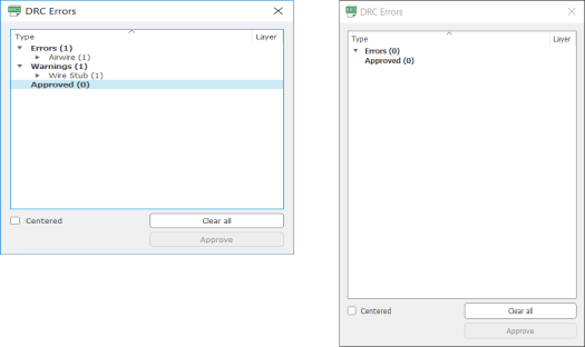
Then after loading the DRC script I checked my connections and it appears that I have one error and one warning. Both are not severe, however they might cause problems during the milling process. The error was that I have an airwire, which means there is a connection that is not 100% secure. And the warnning was a wire stub in one of the components. I solved both issues and I checked again for DRC and I was all set.
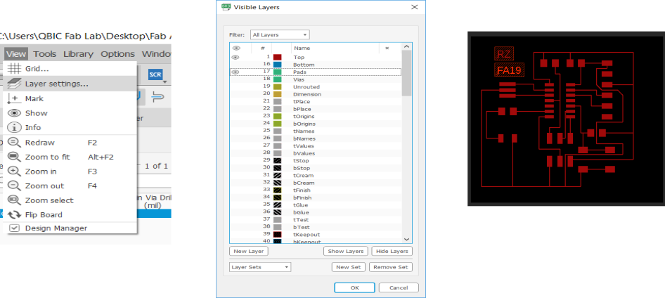
Finally, after finish with the whole proces, I saved the board as an image so I can move it to fab modules to prepare it for the milling process. To covert the PCB to image first I followed the following steps, View - Layer Sitting, and in layer sittings I only showed the top and pad view of the PCB board and hide the rest of layers.
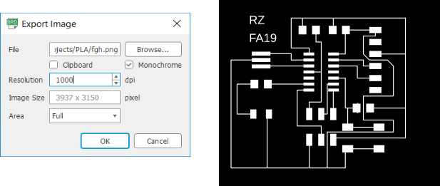
Then I exported the file to an image from File- Export - Image. When exporting to an image it is important to increase the resolution to 1000 or above, and to enable the monochrome option so the image of the PCB can be imported as black and white.
PCB Milling
To start the milling process first I need to prepare my PCB file before sending it to the machine. To do so I used MODS.
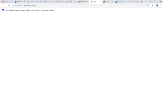
MODS is the upgraded version of FABMODULES, it is more capable and works by connecting nodes to develop each process. It is easy to customize the workflows by loading different modules or use an already precompiled program.
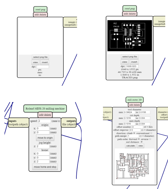
To prepare the milling file there is two main stages; loading the program module, and load the PCB image to start the process. Therefore, first I used already precompiled program that would prepare the file I will upload to be milled using Roland. To do so I right clicked on the screen, choosed PROGRAMS > OPEN SERVER PROGRAM > ROLAND > MILL > MDX20. Even though the machine we have in the lab is MDX-50, the program will still be able to create a file in a formate that our machine will still be able to read it.

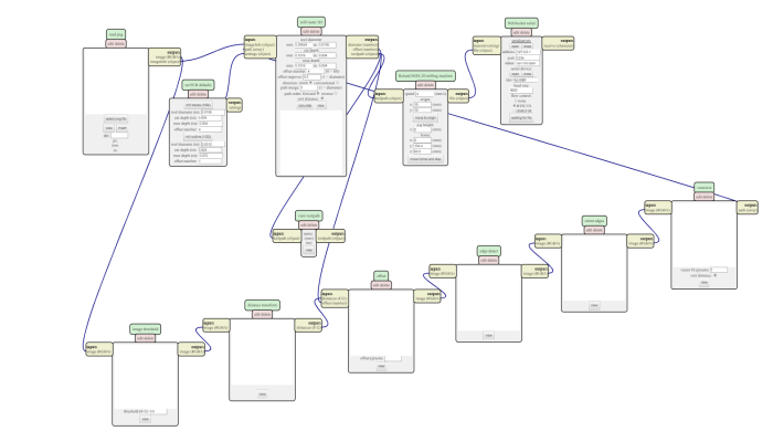
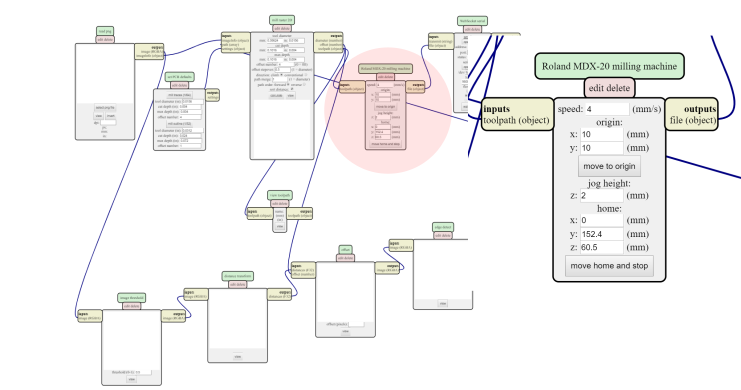
Then after preparing the module that will create the milling file, I should add another module to make to save the file automatically. Meaning that I need to look for the program/component that outputs the file, and connected to the component that will save the file for me in my computer. In this case the component that will output the file is this one:
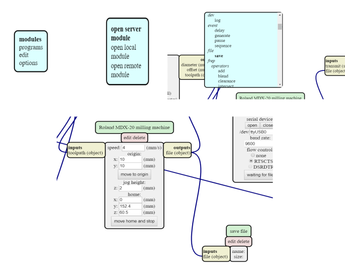
To create the component that will save the milling file: click anywhere in the white space and select MODULE > OPEN SERVE MODULE > SAVE FILE, and then I connect it to "Roland SRM-20 milling machine " component by clicking onec in its output and the input of the "save" component.
After preparing the prcompiled program, I uploaded my file which is the image of the PCB, and change the parameters according to our machine setting, to finalize the milling file.
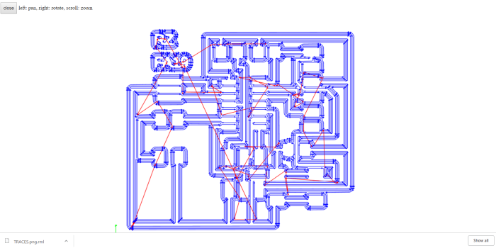
When the software is done with calculating the travels of the machine, a screen will pop-up showing the machine travel over the traces, and the file will be automatically downloaded to the computer. By this the file will be ready for the machine, and the next thing to do is strat the process of milling the PCB board.
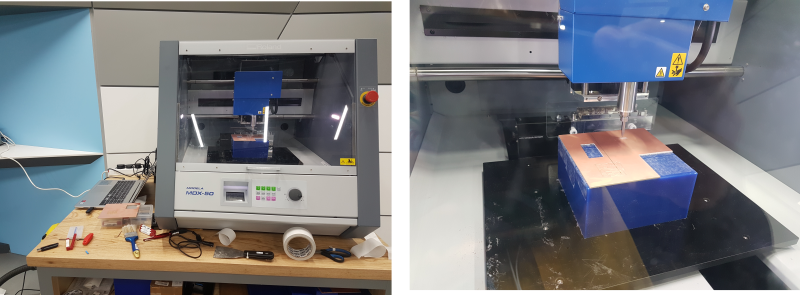
Finally I started the milling process by uploading my file to the machine. The milling time was around 20 min, I did not expect it to take that long specially that last electronics assignment the boards did not take more than 10 min. However, I had to wait longer this time to see how my master piece turned out :).
At the begining I had problem with the milled PCB. The traces seemed neat, however I had short circuit at different place of the board. At the beginning I tried to remove them manually, but it was not a success. Therefore, I decided to repeate the process againg and change the design a little bit to see whether it is going to work.
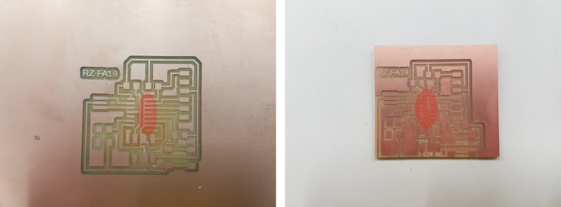
Finally I was successfully able to solve the short circuit problem by changing the initial design I had, and by playing a little bit with the bit I was using to mill the PCB. And by this I was done with the milling process and the only thing left to do is to solder the circuit and finally program it.
PCB Soldering and Testing
After I finished from fabricating the PCB I started the finaly steps of the assignment which is PCB soldering and testing.
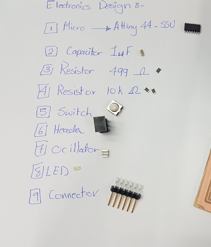
The electronics list was the following:
1. Attiny 44 microcontroller.
2. Capacitor 1uF.
3. Resistor 499 ohm.
4. Resistor 10k ohm.
5. Switch.
6. Header.
8. Oscilator.
9. LED.
10. Connectors.
Then I prepared my soldering station to start the process and solder my PCB.
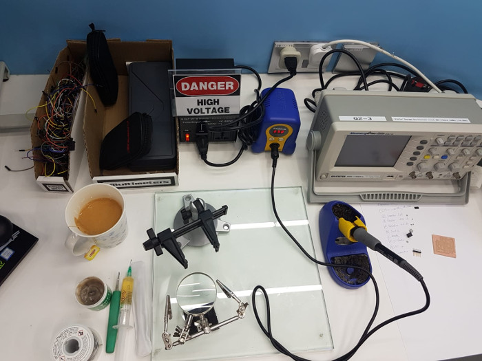
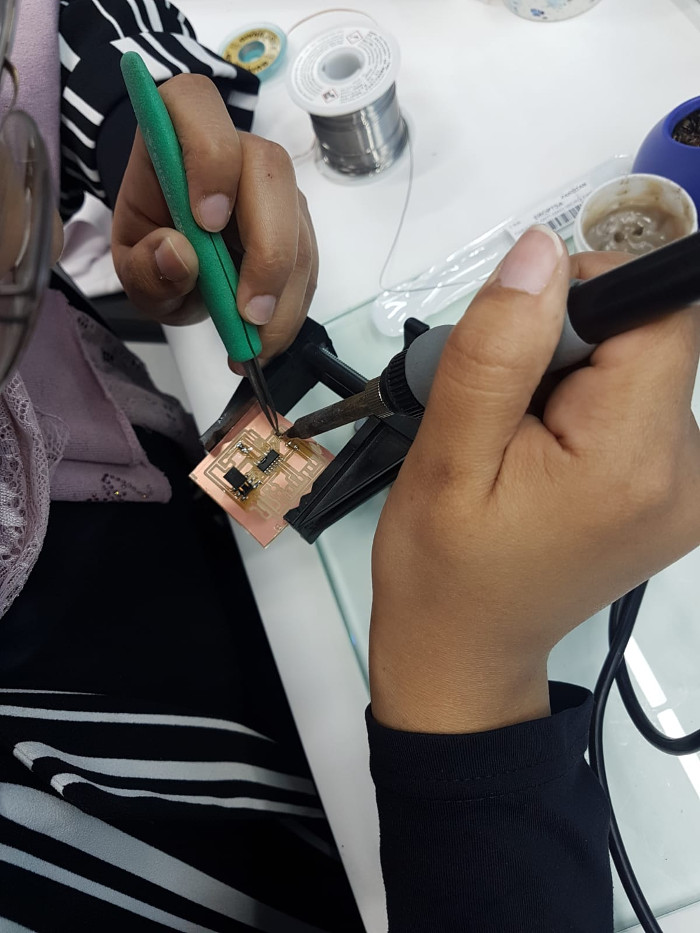
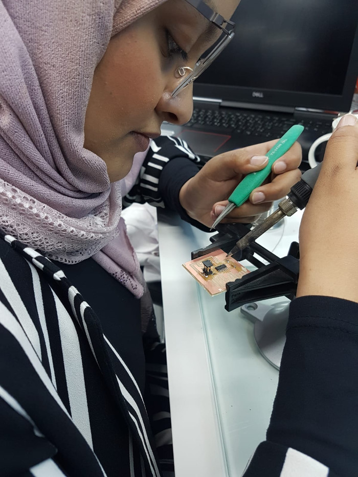
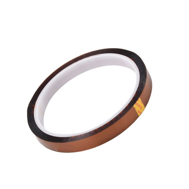
The first PCB I soldered was a total failure. I tried to program it over and over again with no luck. I read about it and there were different reasons why it might be the case, and it turned out that maybe because I was over heating my Attiny 44 microcontroller I dameged it. Therefore, I decided to do a new PCB and be very careful when soldering it, and I used polyimide tape as soldering shielding to prevent the over heating issue.
And the PCB worked perfectly!!
