Task 7
Electronics design
In this week, I was given a task to have a group assignment and an individual assignment. The group assignment was to use the test equipment in your lab to observe the operation of a microcontroller circuit board, and the individual assignment was to redraw the echo hello-world board), add (at least) a button and LED (with current-limiting resistor), check the design rules, make it, and test it
Individual Task : Redraw the echo hello-world board
For this week, I was required to redraw the echo hello-world board and add atleast a button and an LED. I decided to utilize Antti Mäntyniemi Schematic design for this purpose. I decided to use Eagle from Autodesk.
Getting Started with Eagle
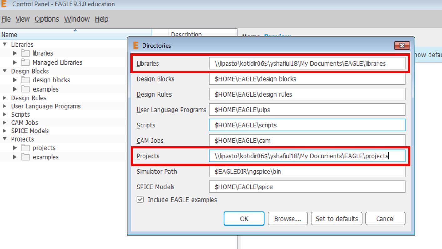
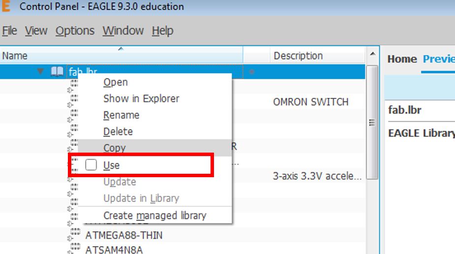
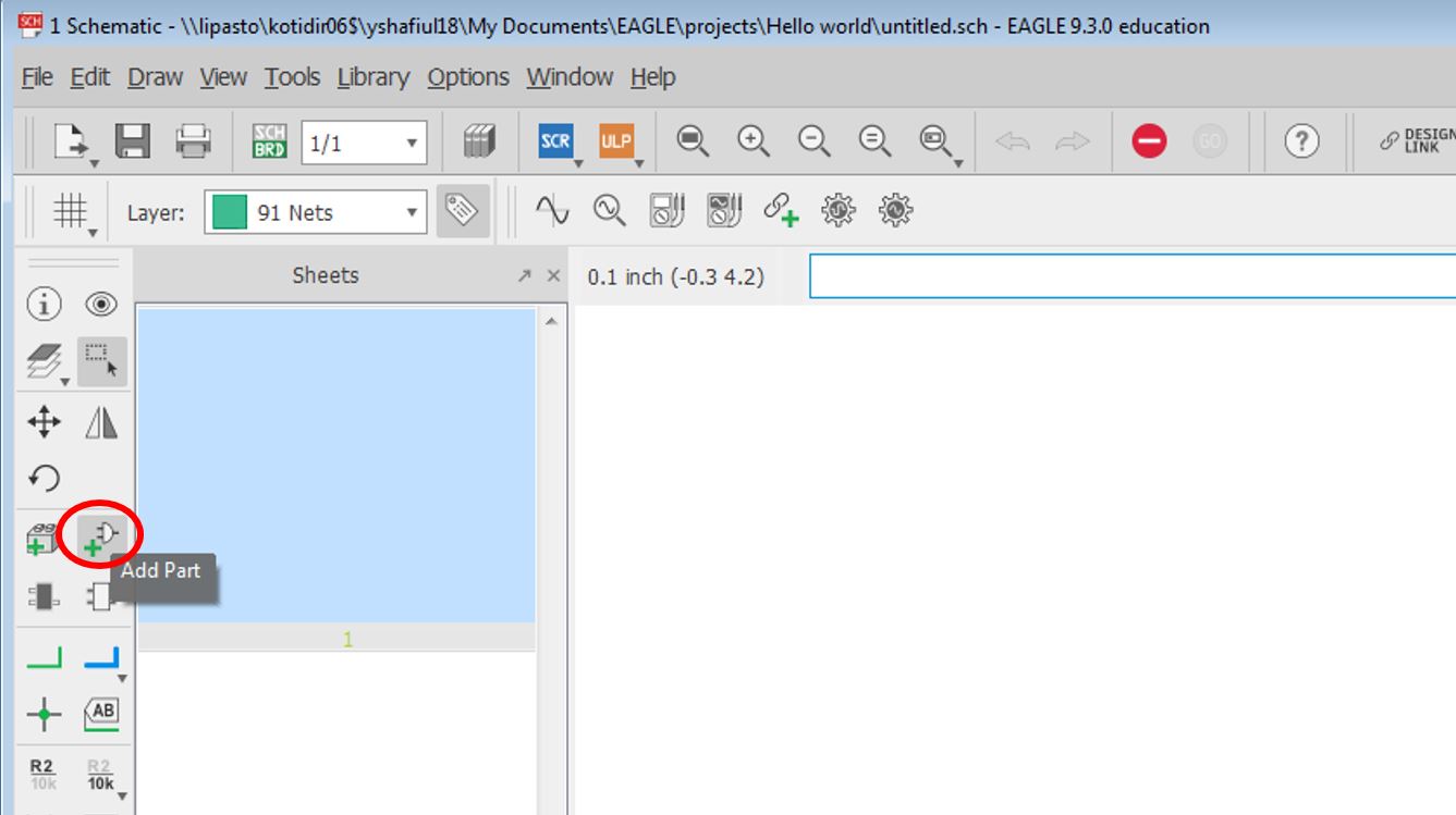
At first, I download the Eagle Software from the Autodest Website. I downloaded the fbr.lbr file which was the required FAB LAB library for Eagle Software. To Add the Library, Paste the fbr.lbr in Eg: (c:\\My Documents\EAGLE\libraries). The fbr.lbr will appear in the Libraries in Eagle. Go to Options-->Directories-->Add the Library path for Libraries and Projects.
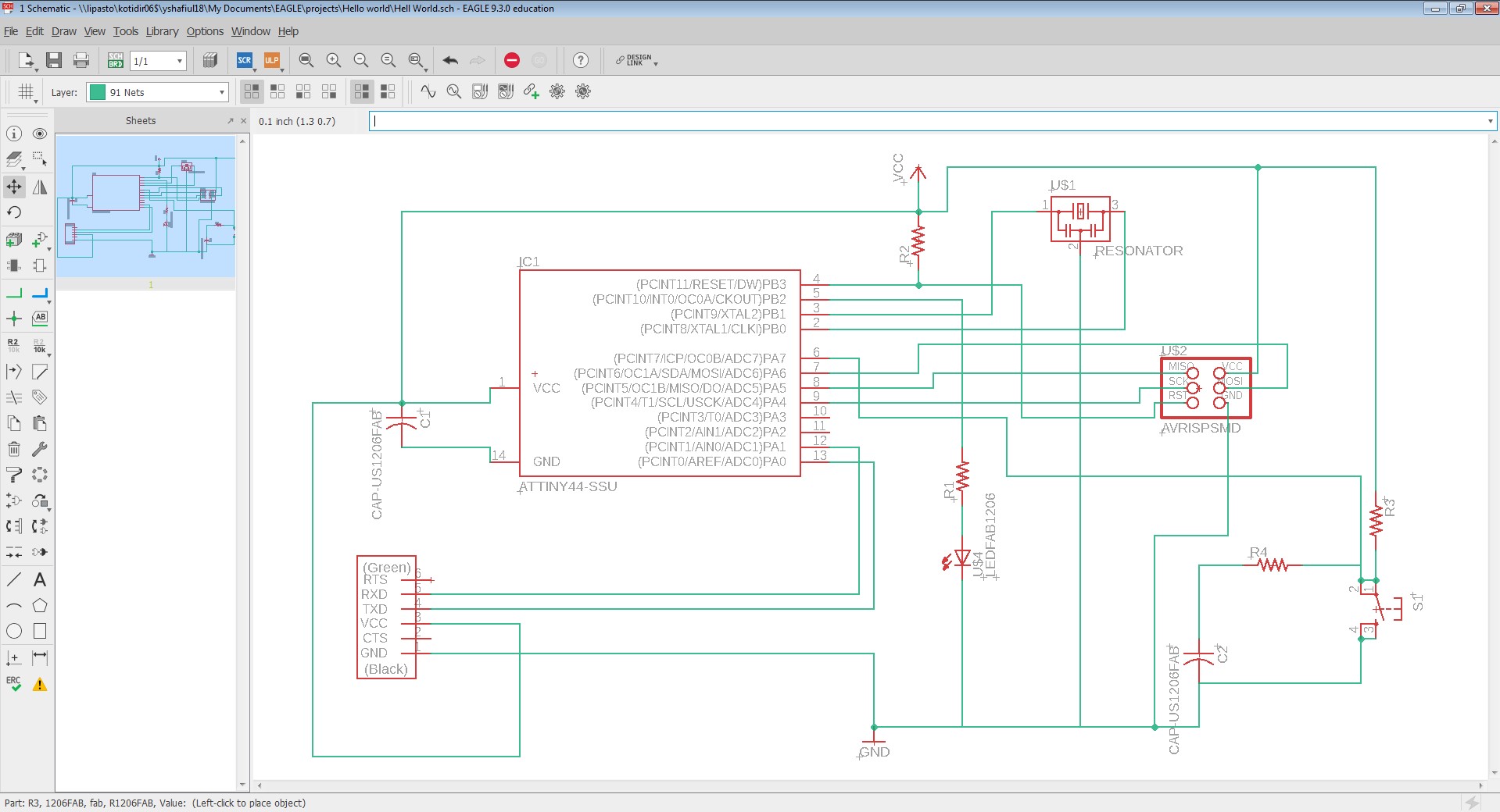
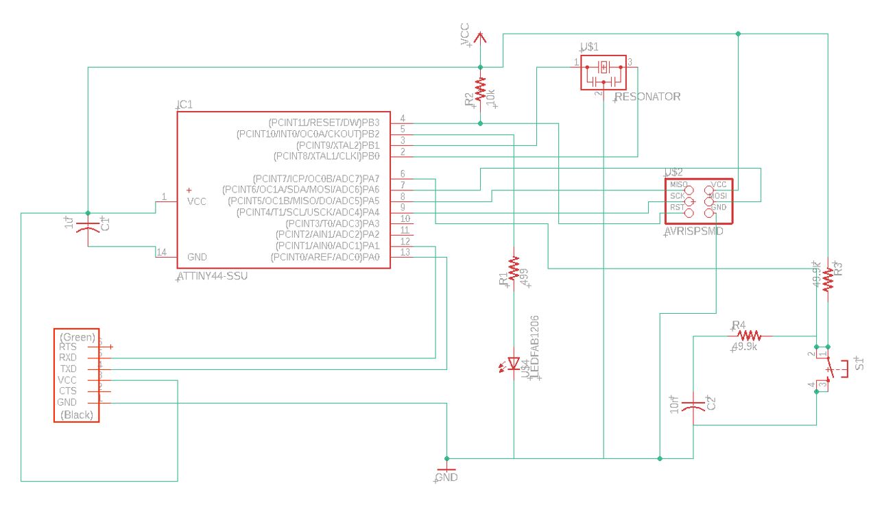
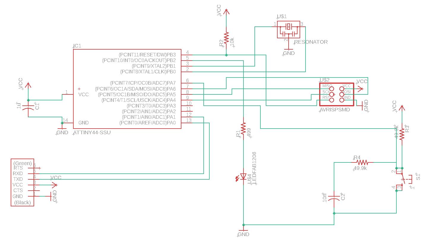
Schematic Design
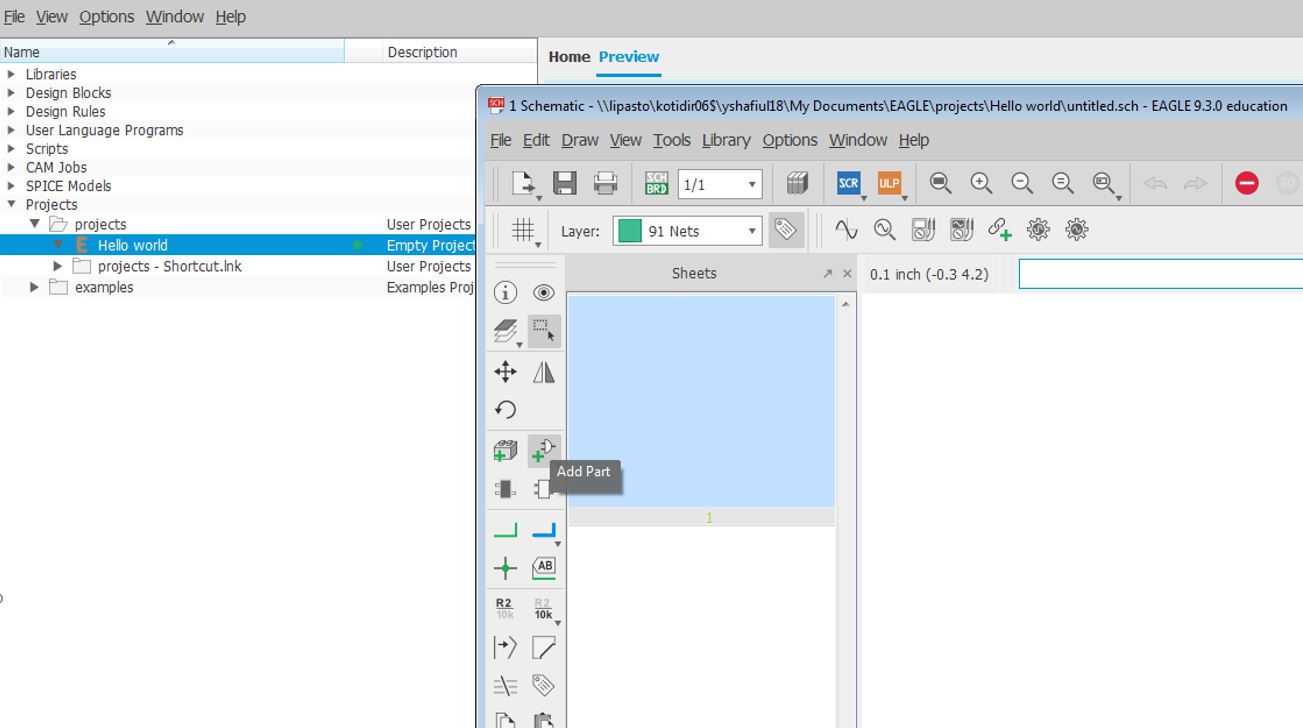
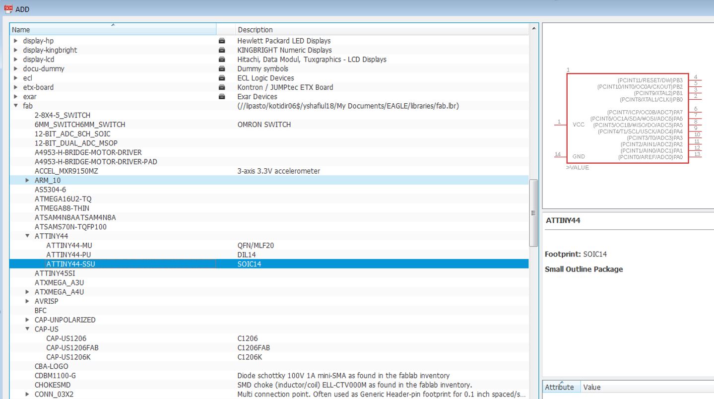
- I collected all components to get from the Library, The necessary components are:
- 1x ATTiny44-ssu (fab> ATTINY44)
- 1x Resonator (fab)
- 1x AVRISP SMD (fab>AVRISP)
- 1x FTDI SMD Header (fab)
- 1x 10 nF CAP-US1206FAB (fab--CAP_US)
- 1x 1 uF CAP-US1206FAB (fab--CAP_US)
- 1x Omron switch B3SN-3112P (fab)
- 1x LED FAB1206 (fab)
- 1x 499 ohm RES-US1206FAB (fab-->RES_US)
- 2x 49.9k ohm RES-US1206FAB (fab-->RES_US)
- 1x 10k ohm RES-US1206FAB (fab-->RES_US)
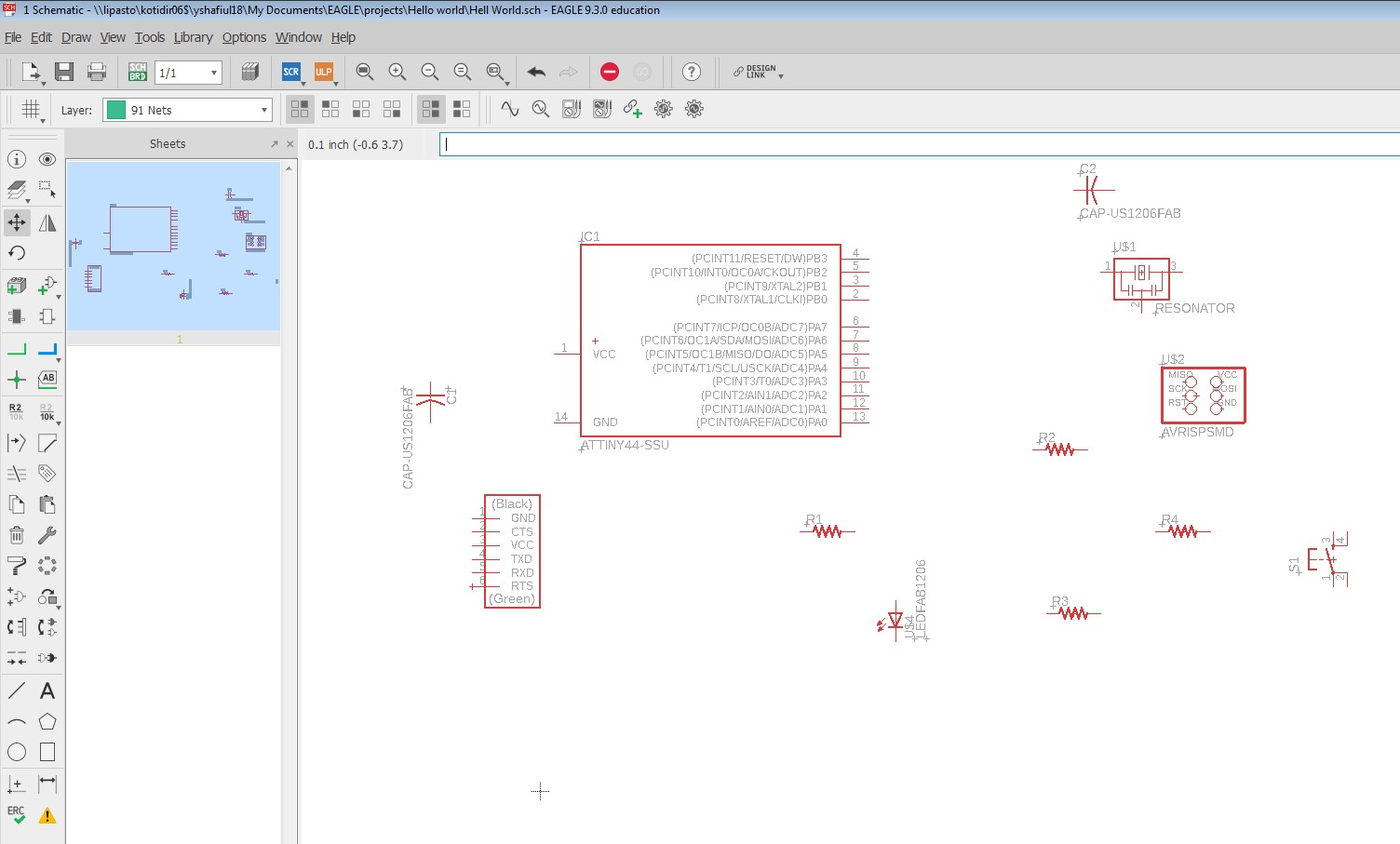
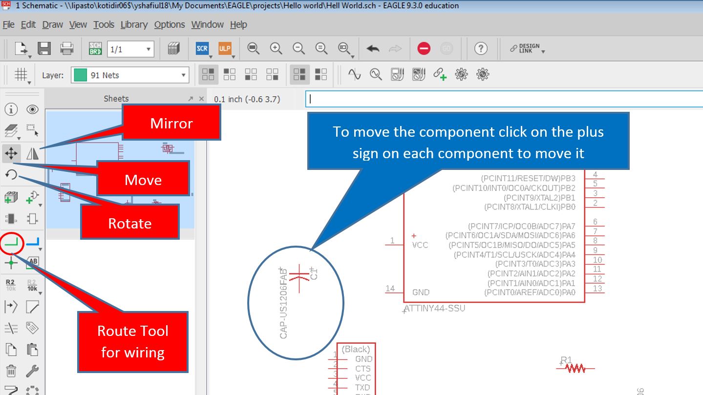
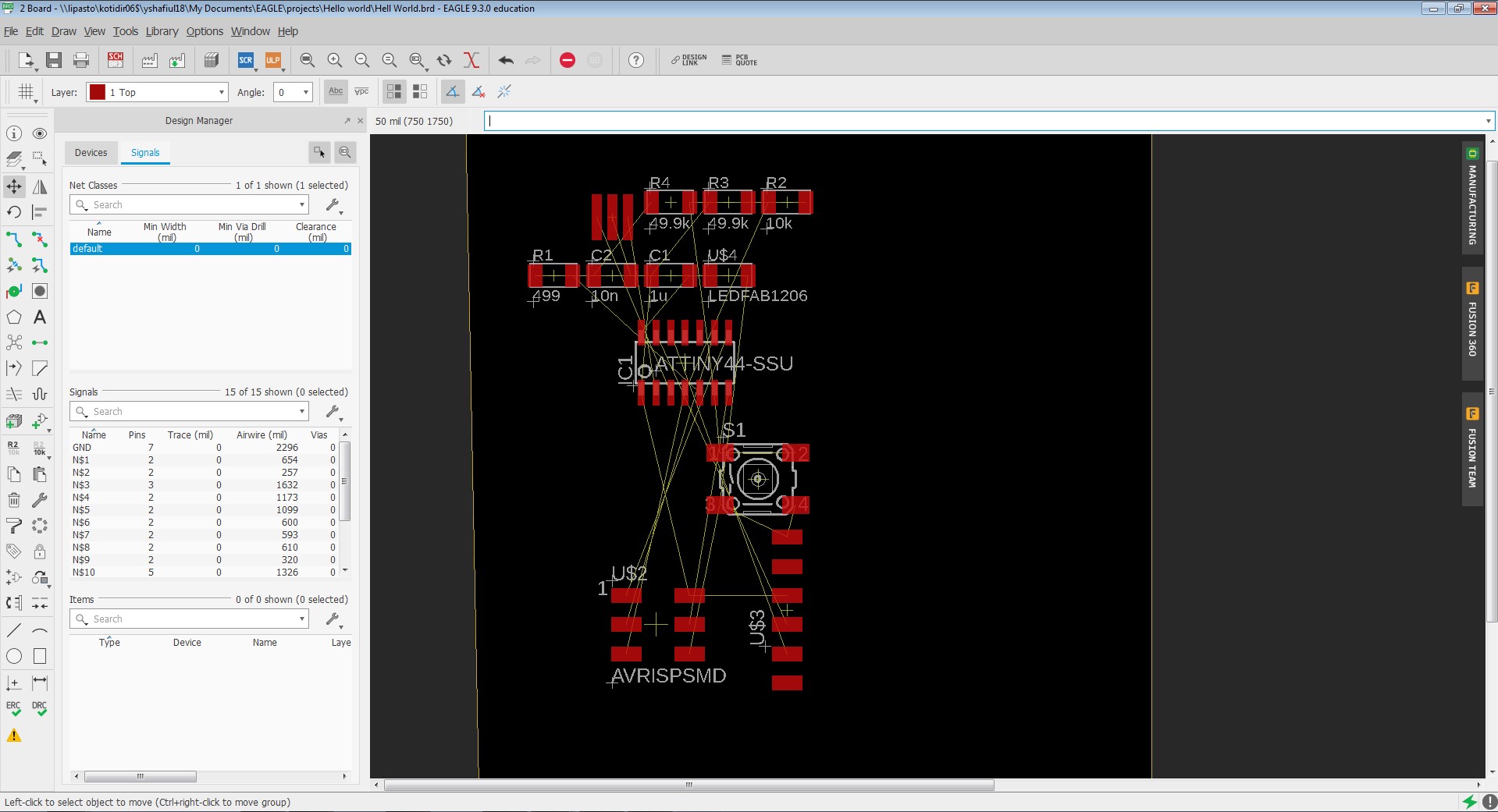
I selected the components one by one and placed it in the Schematic Window roughly. Then I used the route tool to connect all the components in place.
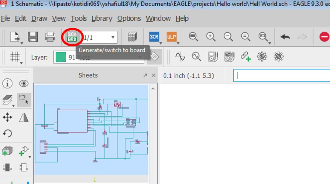
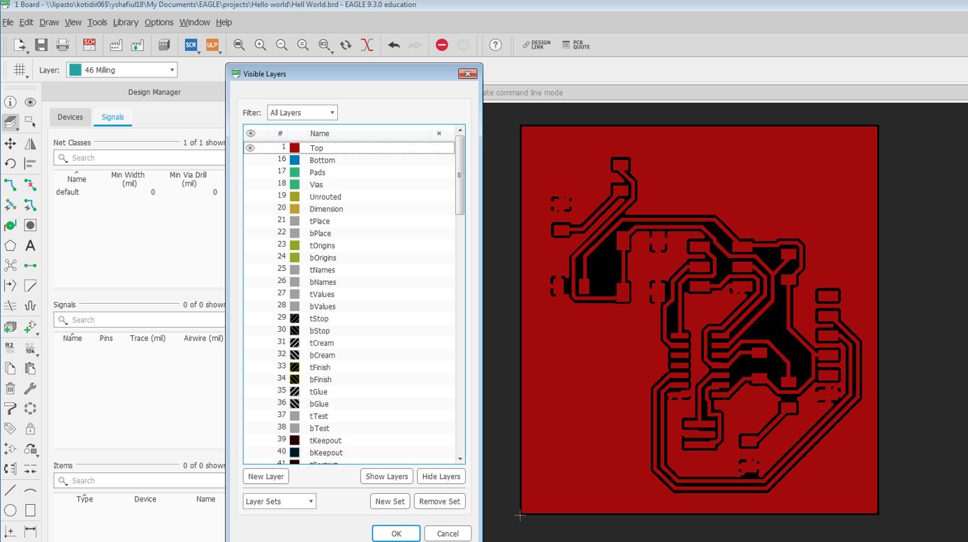
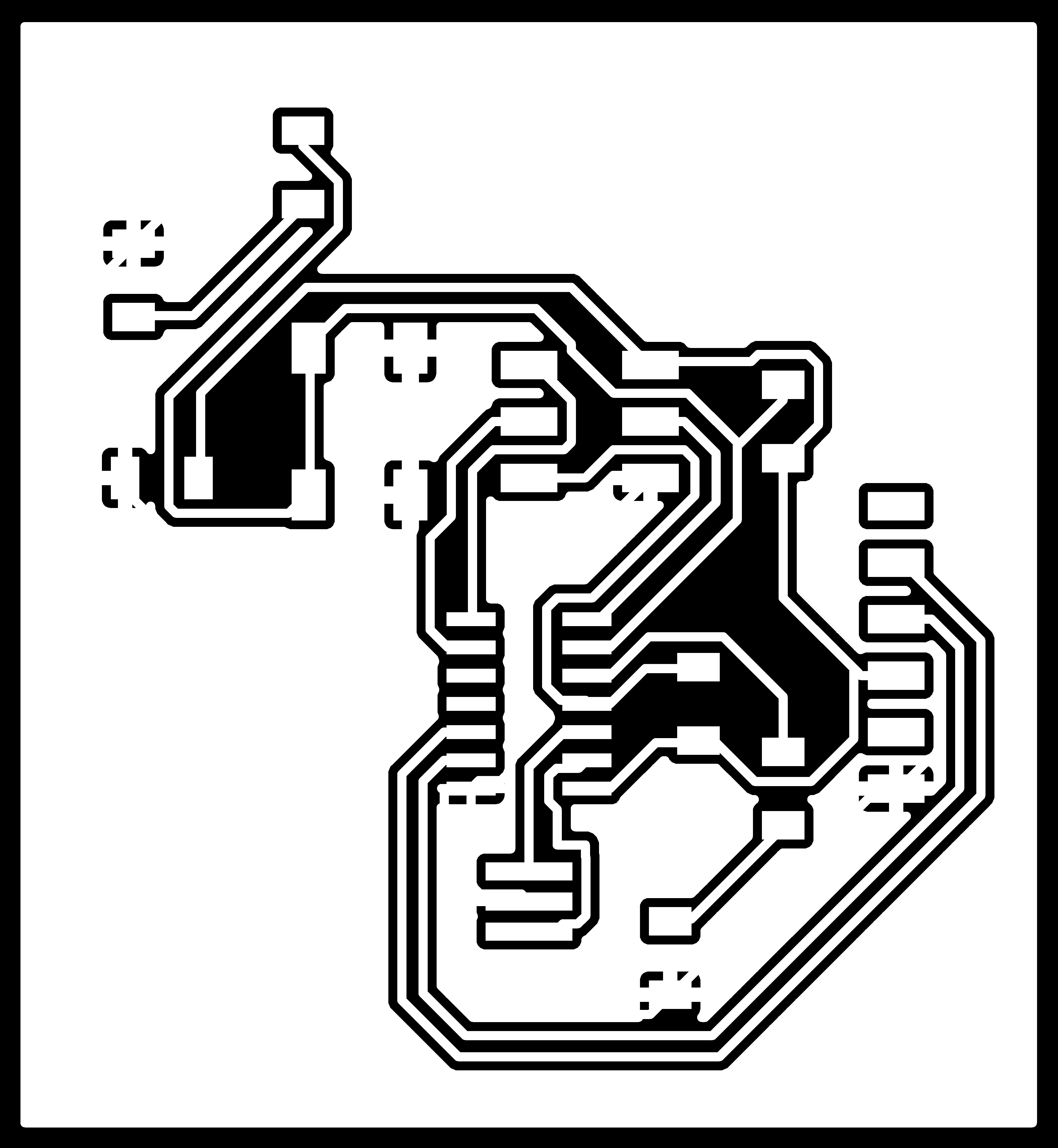
Layout Design
After completing the Schematic, we will move from Schematic to Layout using the SCH-->BRD Button.
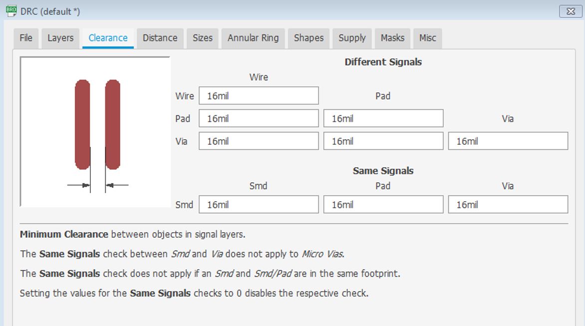
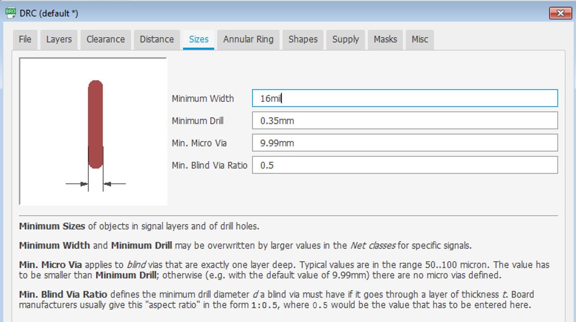
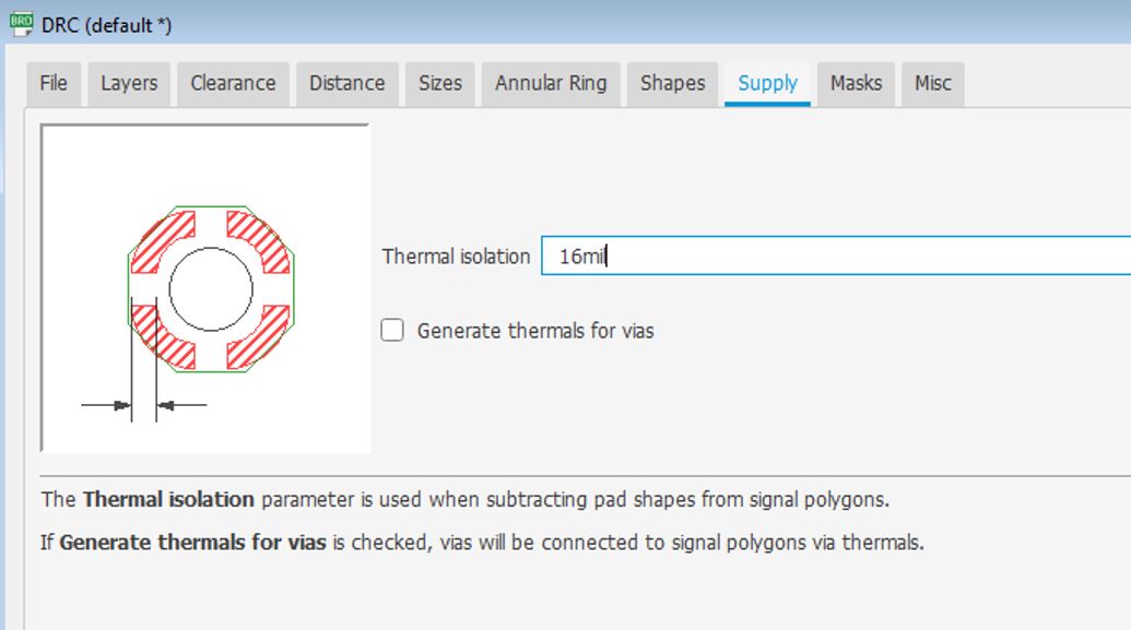
Below DRC Settings need to be ensured depending on the Mil Bit we are using for milling the PCB Layout.
Utilize the Mirror, Move, Rotate and Traces tool to make connections in the Layout.
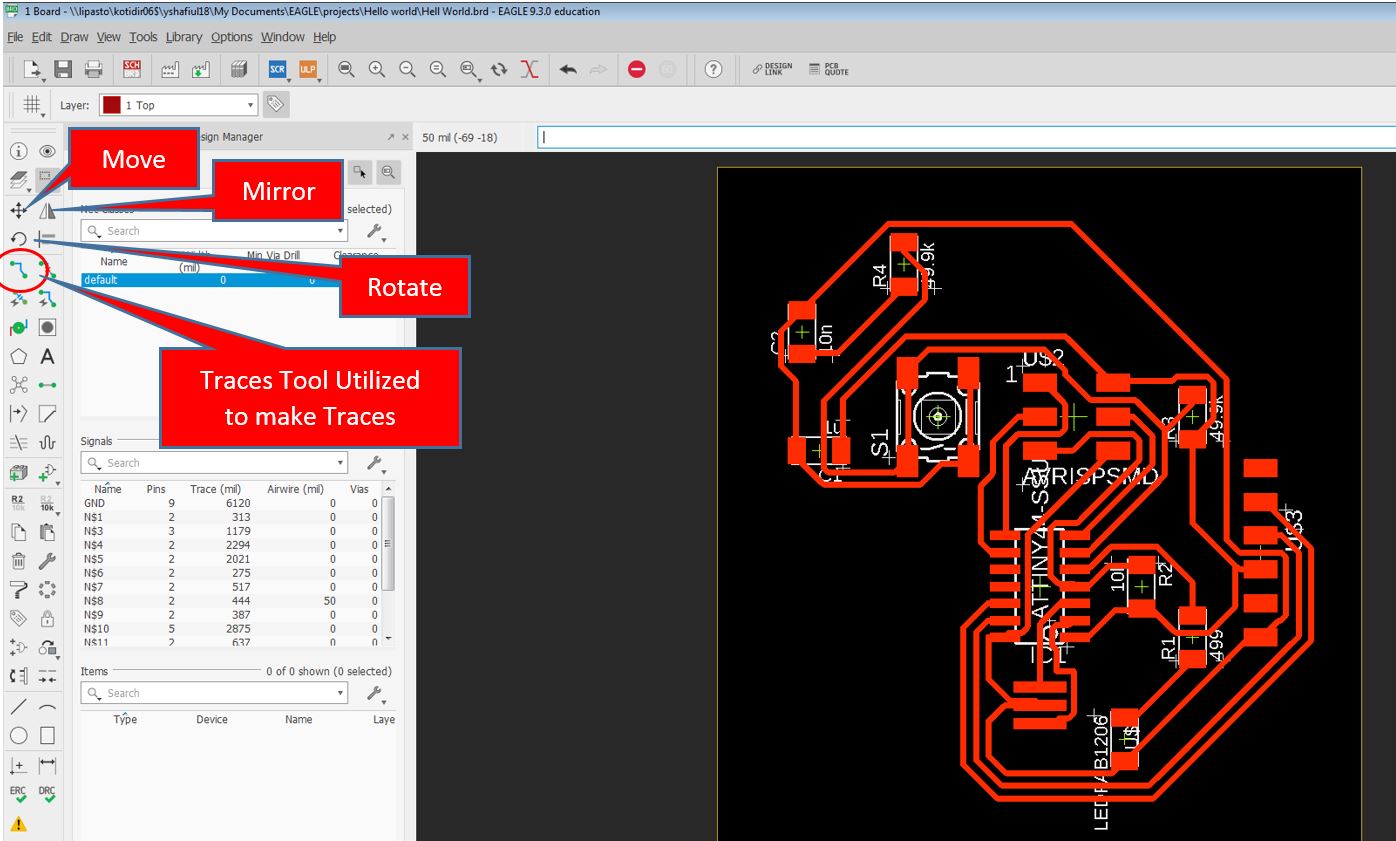
- After Connecting the components, the next idea to make the ground plane which shall be a copper plane surrounding the below components and the traces. To make the Ground Plane follow these steps:
- Draw a polygon around your board (Using Draw-->Polygon) with the name GND
- Utilize (Tool--> ratsnest) to make a uniform plane around it which will connect all the GND with that plane
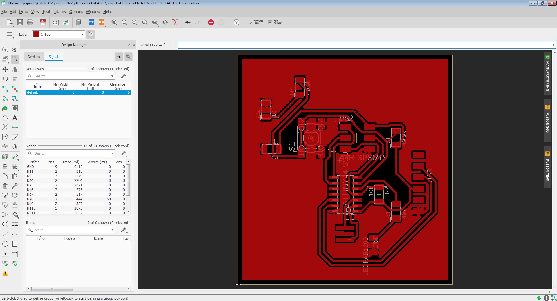
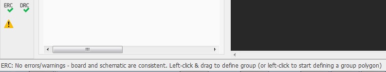
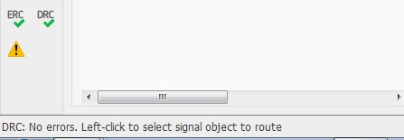
Our Layout design is ready, we need to check for ERC and DRC Errors
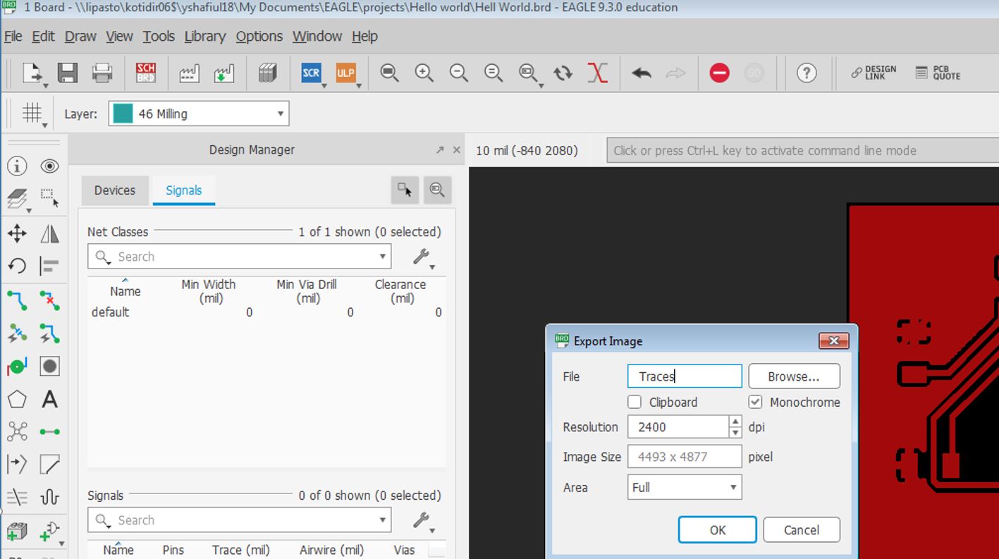
Layout Design Export
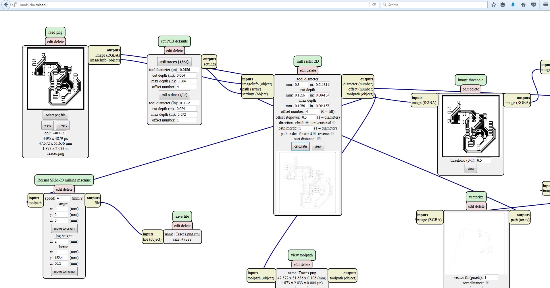
The next step is to export the layers in the png format
- For Traces:
- Select on the Top Layer
- Export Image with High Quality [Select : Monochorome, Resolution : 2400 dpi]
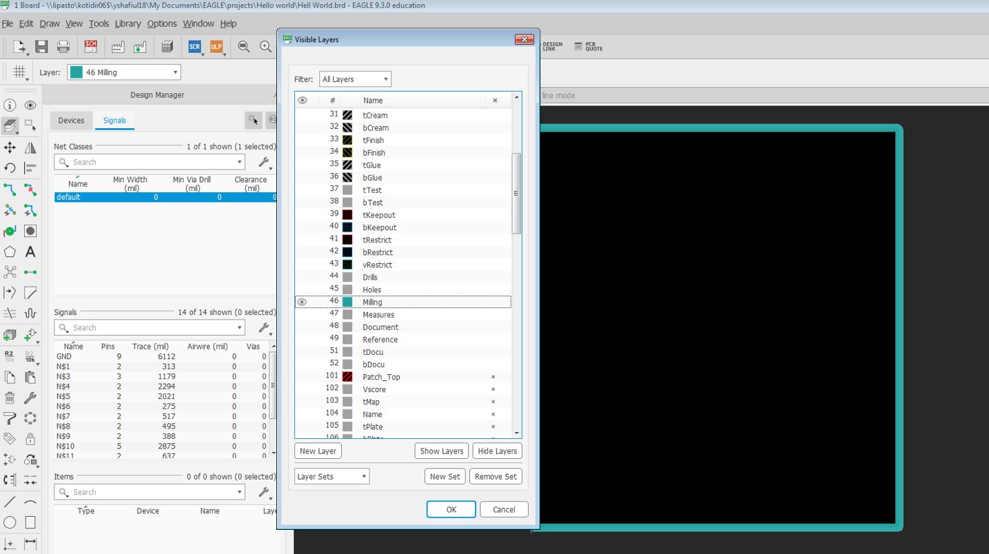
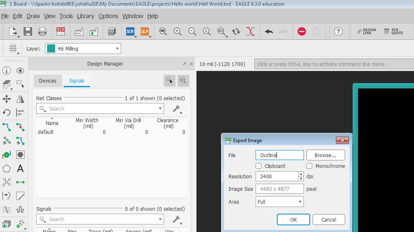
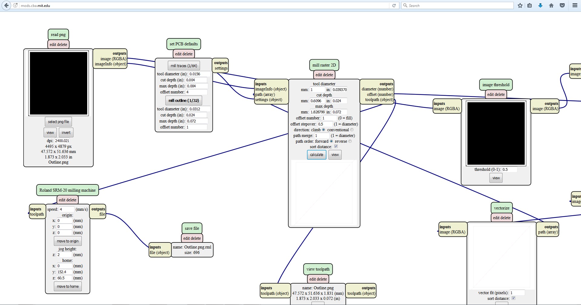
- For Outline:
- Make a Milling layer outide the board
- Uncheck all the layes and select the Milling layer
- Export Image with High Quality [Select : Monochorome, Resolution : 2400 dpi]
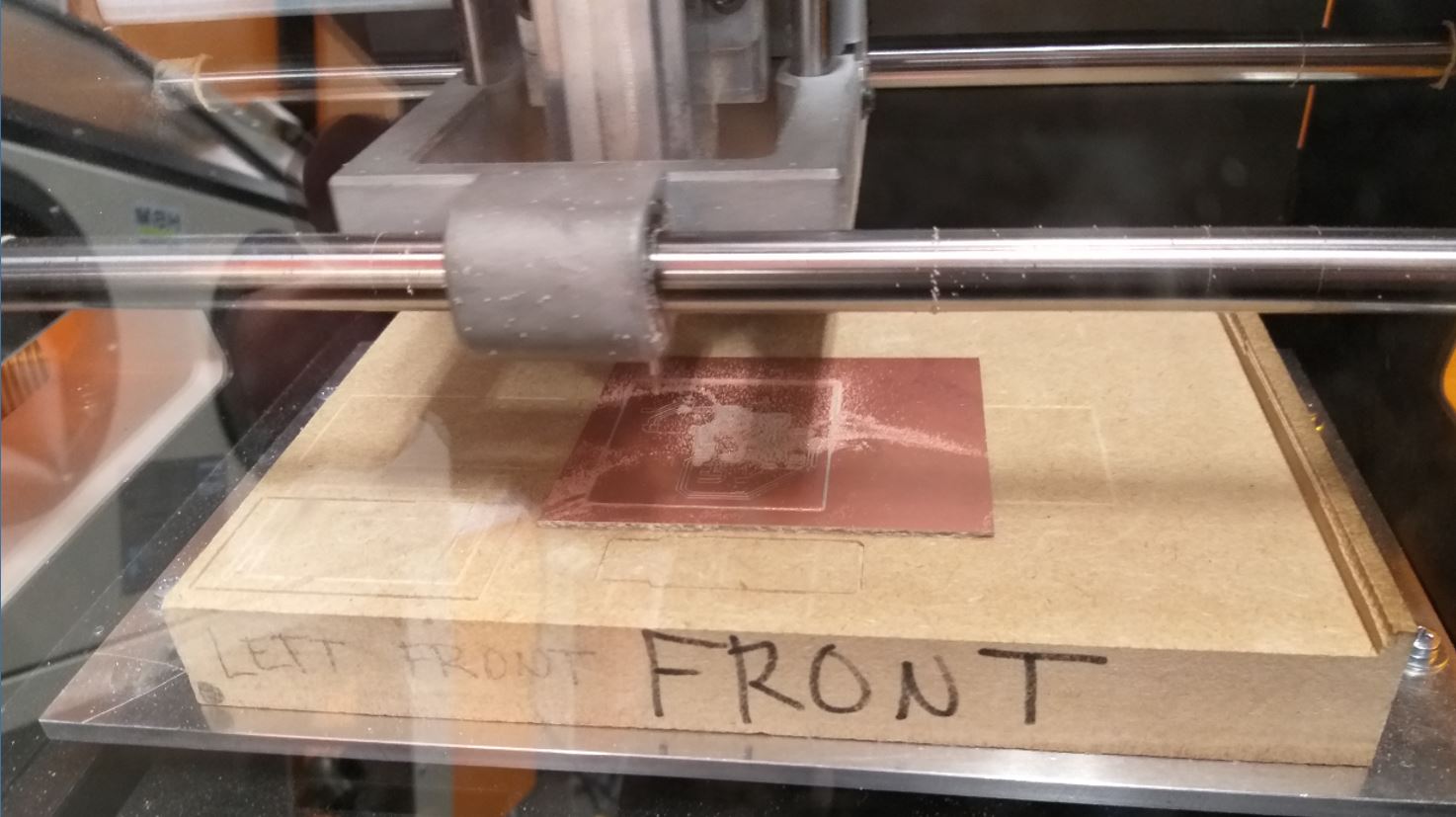
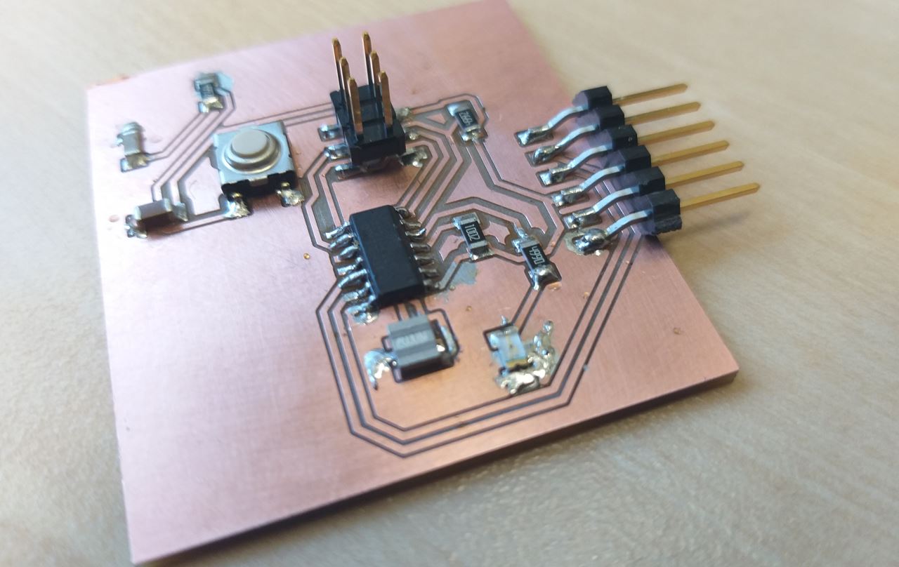
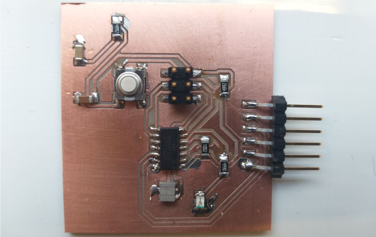
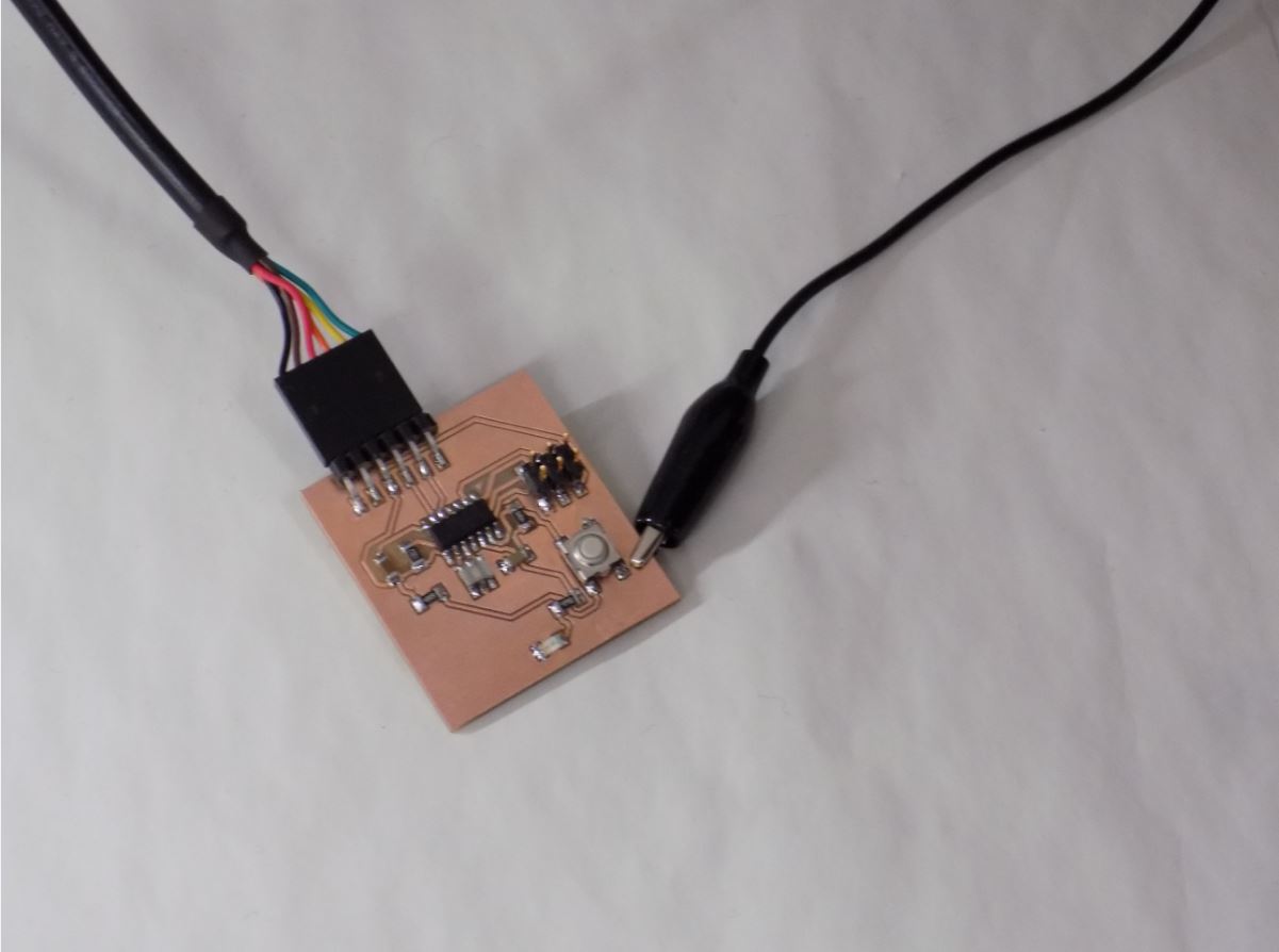
PCB Mill and Solder
Next I Proceeded as in Task 05. I went to fabModules website to work on the traces and outline .png files, to include the milling machine specifications so that the board comes out right.
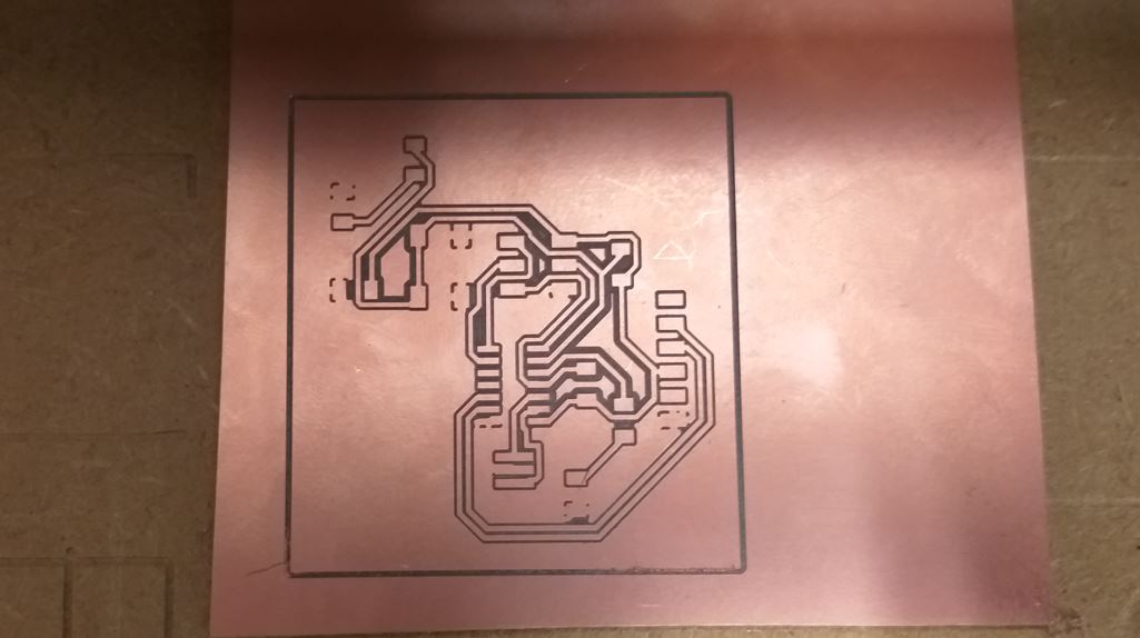
- The required components as used in the schematic as well are:
- 1x ATTiny44
- 1x Resonator (20 Mhz)
- 1x AVRISP SMD (2x3 pin header)
- 1x FTDI SMD Header (1x6 pin header)
- 1x 10 nF
- 1x 1 uF
- 1x Omron switch B3SN-3112P (6mm)
- 1x LED (RED)
- 1x 499 ohm
- 2x 49.9k ohm
- 1x 10k ohm
Programming : Group Assignment (Jobin's Board)
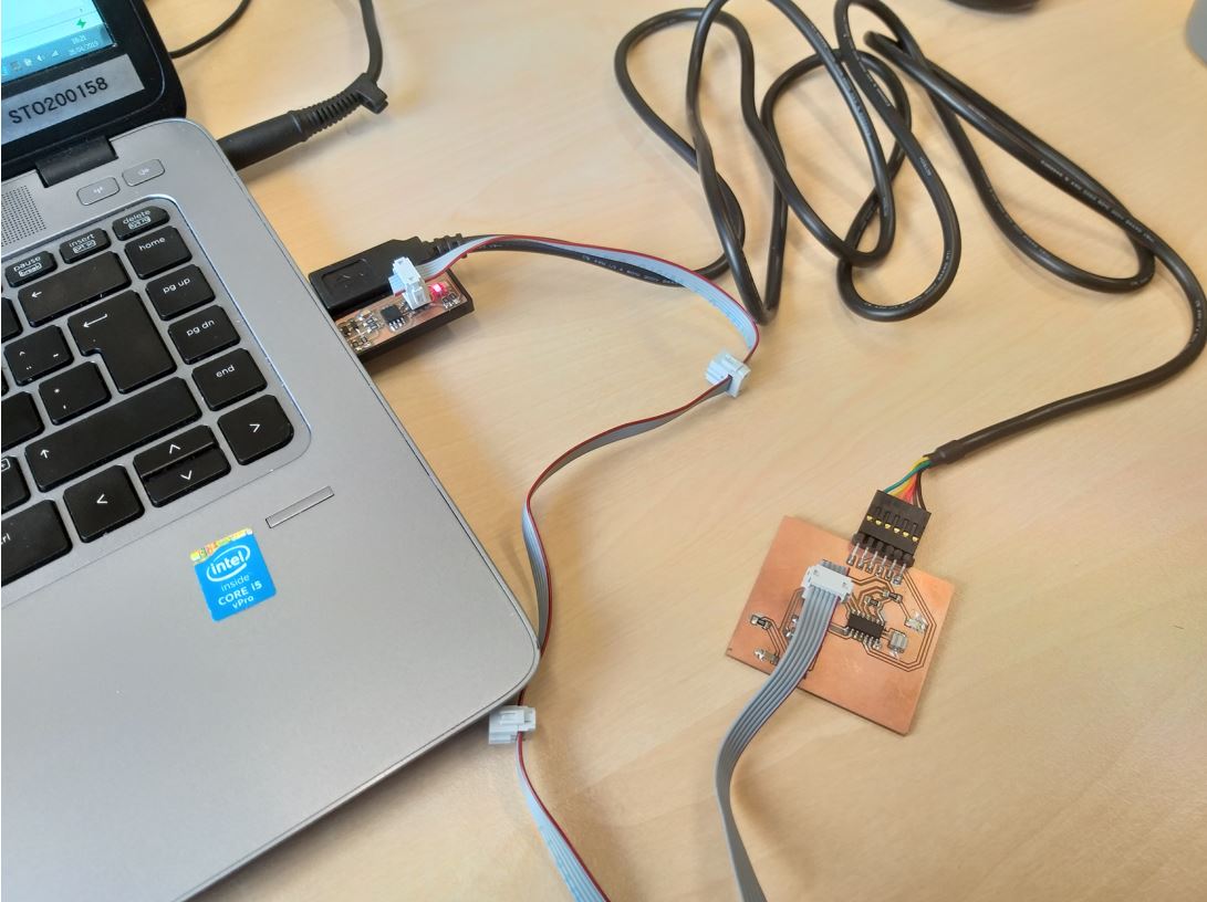
For programming, I utilized the ATTiny programmer that I made in Task 05. I went to fabModules. An ISP cable was connected to the programmer to the new board and ftdi cable (5V) to connect the new board to the computer. Below files are required to download:
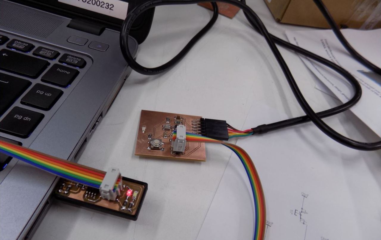
I utilized GIT bash for the programming. I opened the the folder where I had stored my code and makefiles. As a Group Project we used the Jobin. While connecting the new board with an ISP cable make sure that the ground pins are matched. Then connect the new board to the computer with the FTDI cable and the red light will be turned on in the programmer
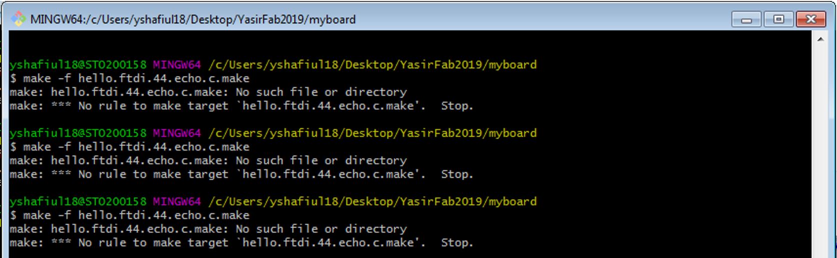
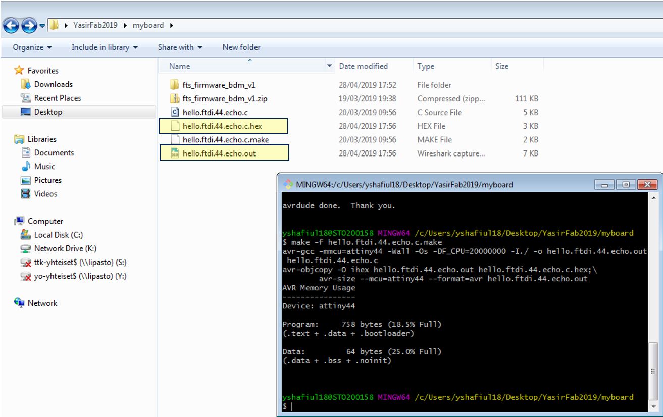
1. Command to make a .hex file for flashing in git bash.
make -f hello.ftdi.44.echo.c.make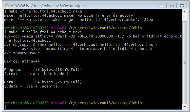
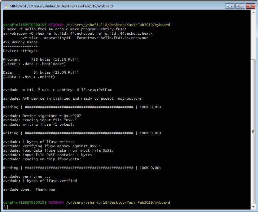
make -f hello.ftdi.44.echo.c.make program-usbtiny-fuses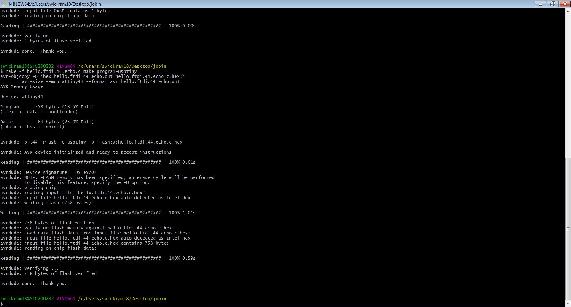
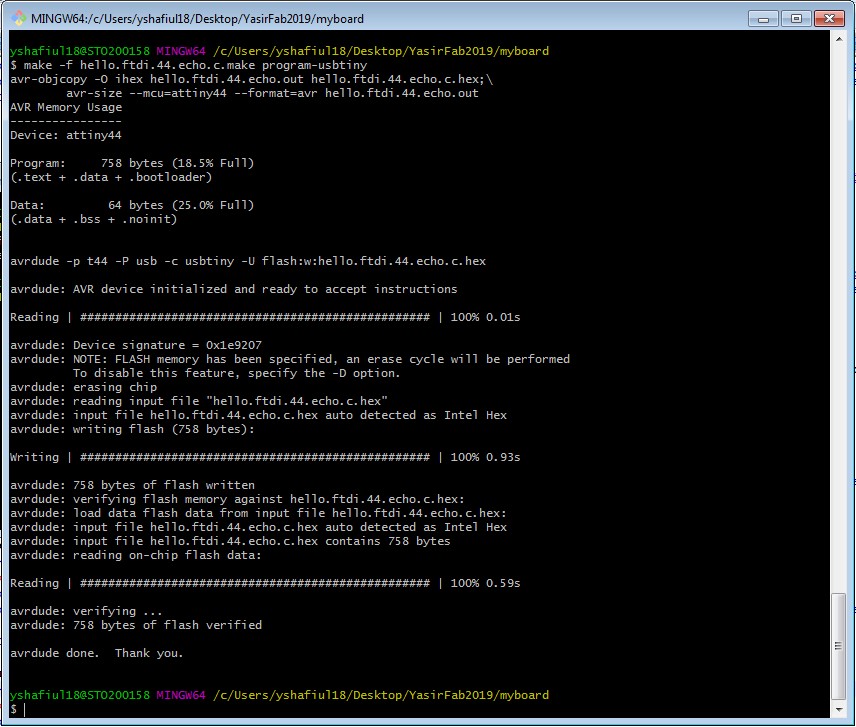
make -f hello.ftdi.44.echo.c.make program-usbtiny
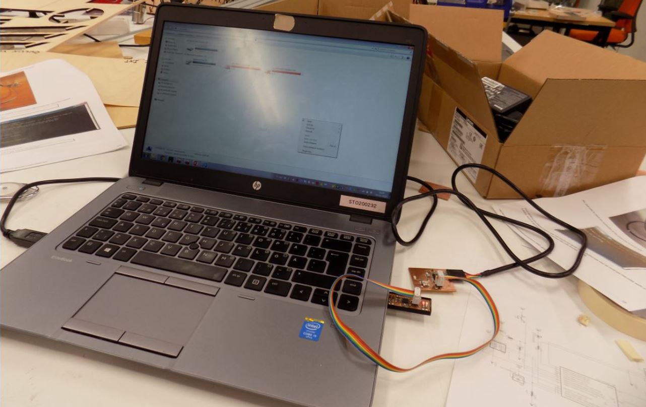
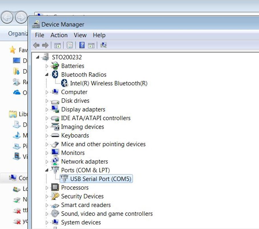
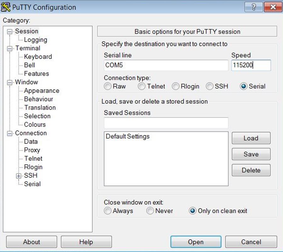
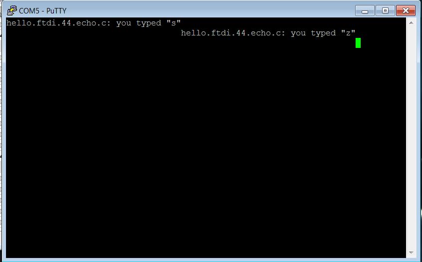
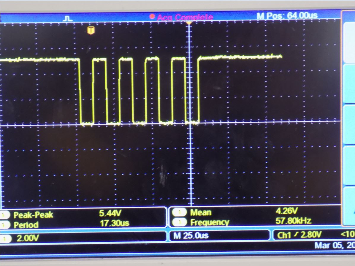
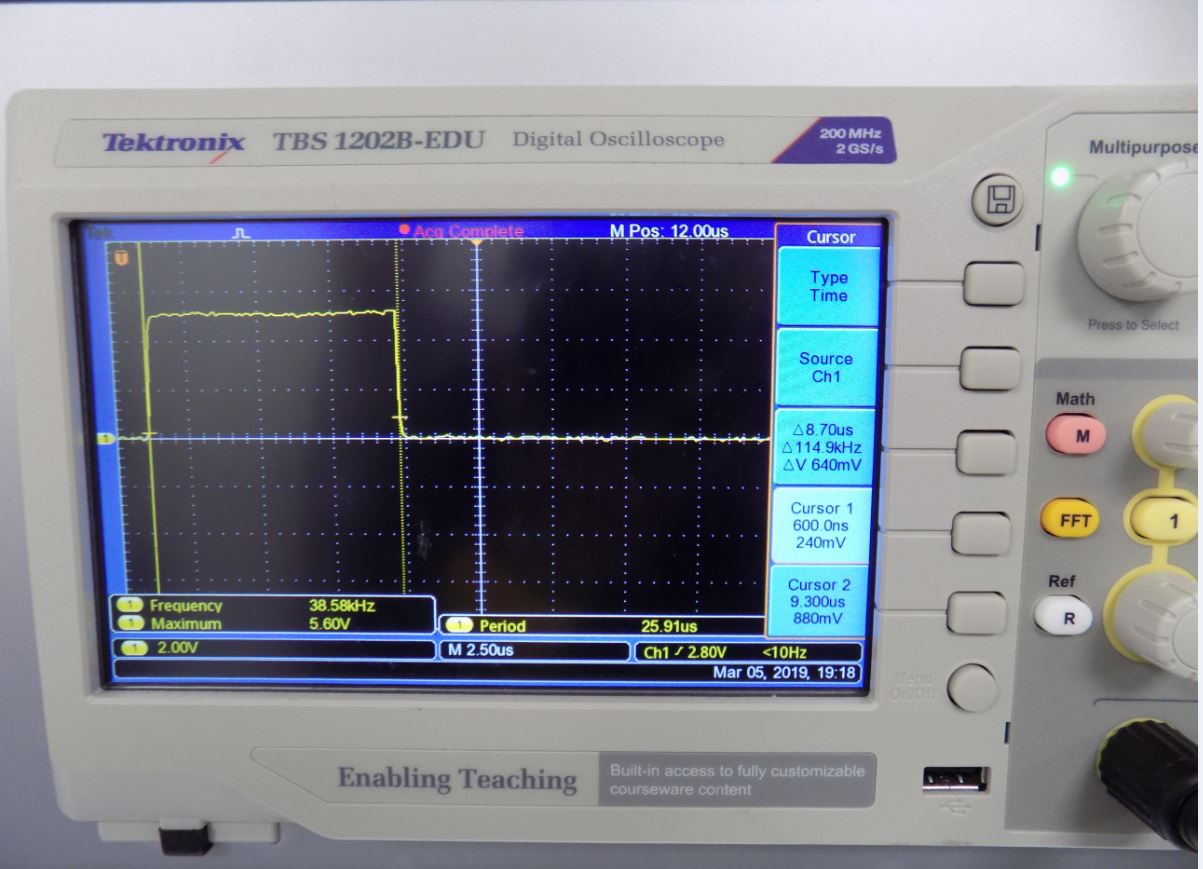
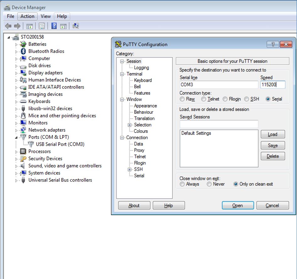
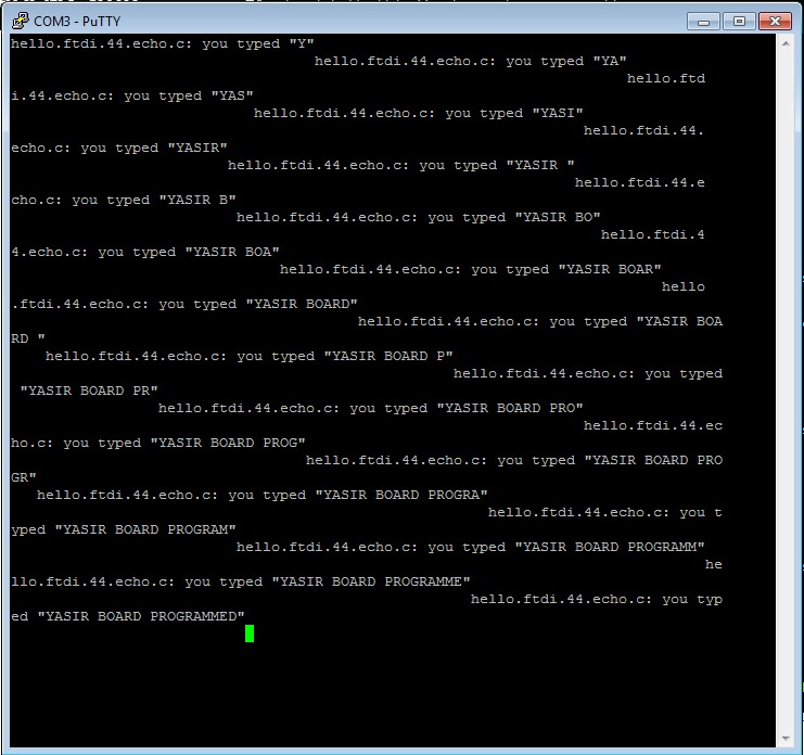
The group work for this week was to observe the operation of a microcontroller circuit board using an oscilloscope. For this case, First We connected the ground plate of the board to the oscilloscope with black wire and the signal probe to serial input (4th in this case) pin. We used putty software to transmit data. To do that we need to check which COMport is connected to the programmer by going to control panel>Device manager. After checking the COMport we open the putty and go to the serial menu. Then changed the COMport accordingly and put the baud rate as 115200 and pressed Ok.
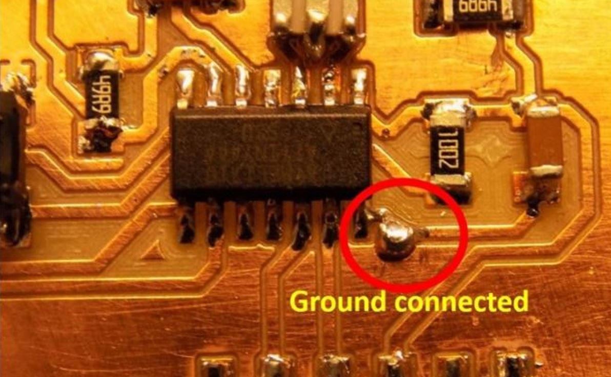
After giving some input on the terminal, unfortunately, putty window hanged and was slow displaying the signal. Our local instructor Antti helped to rectify the problem by finding that the IC ground was not connected properly. After soldering it to the nearest ground it started to work fine.
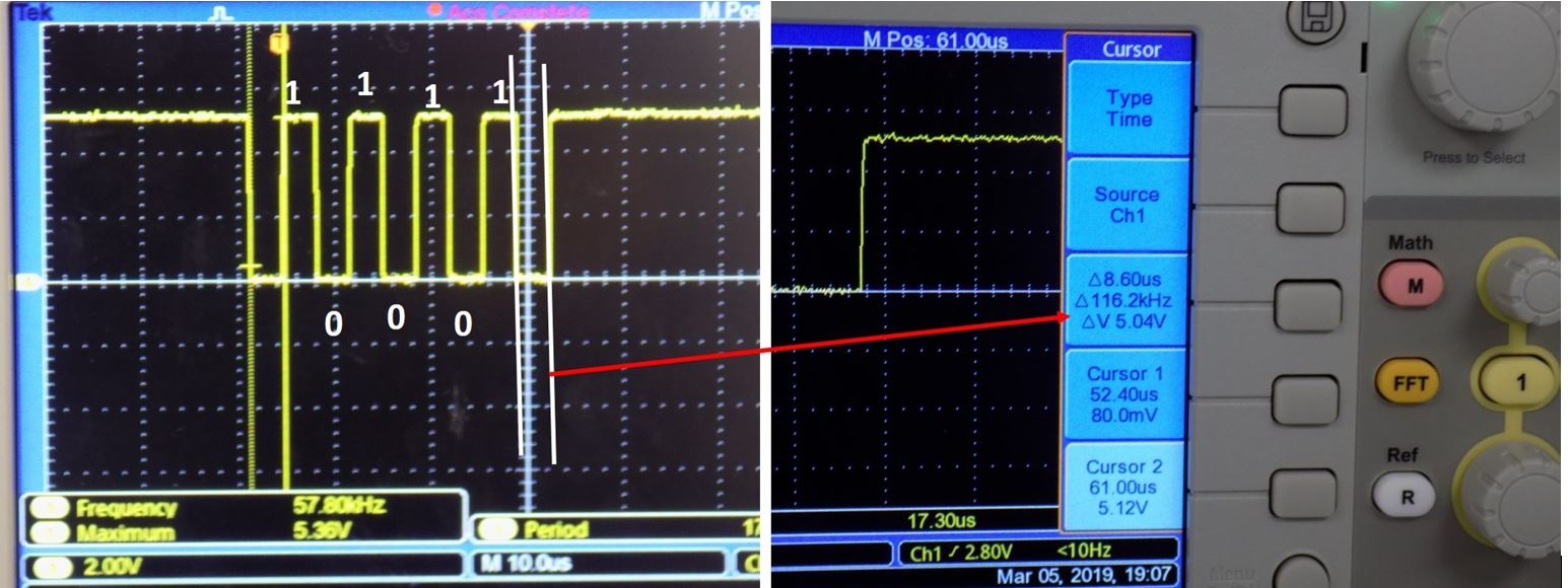
After pressing a command eg. 'U' in the terminal on the oscilloscope view, we could see that pulse width was approximately 8,65us, which was close to the inversed baud rate of the terminal, 115200. Moreover, from the oscilloscope, we could count the bits
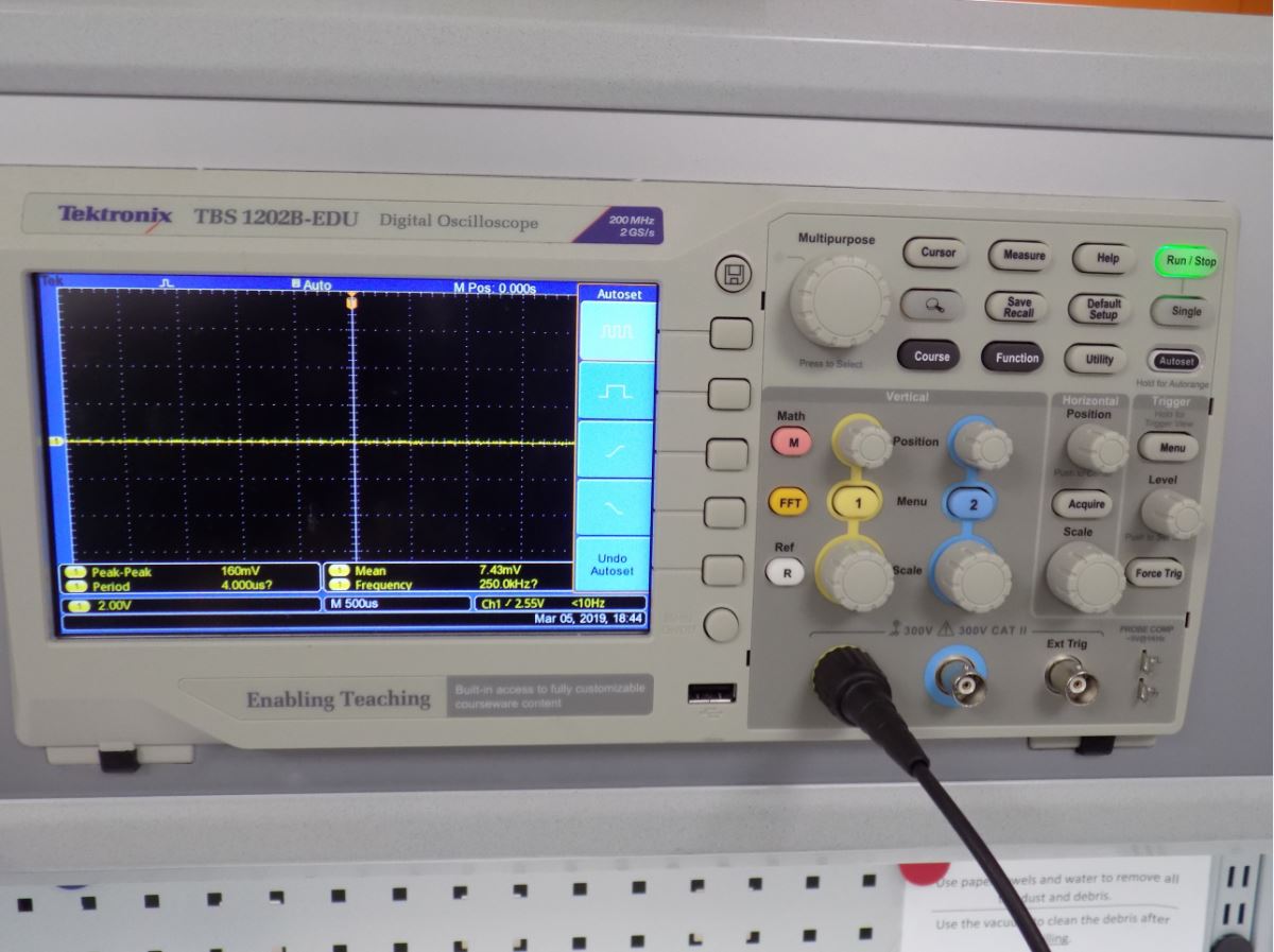
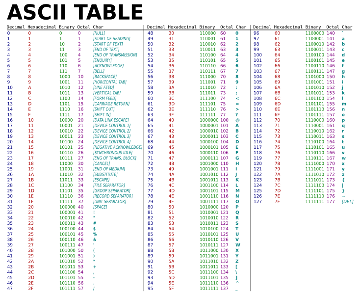
Inorder to translate the bits seen in the oscoloscope to characters, The ASCII Table shall be utilized. As we can see in the below pictures as we press "U" the corresponding binary bits for U = 1010101. which can be seen below
Programming : Individual Assignment (My Board)
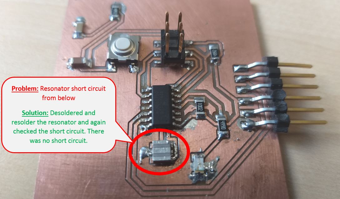
I was facing two problems, due to which I was not able to program my boards earlier. The two problems were: