"" -
Networking and Communications
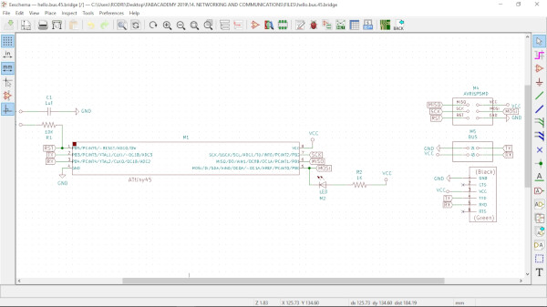
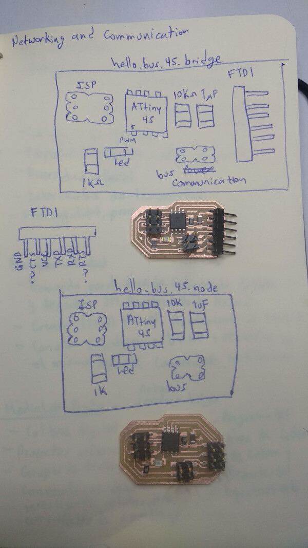
I designed one bridge and one node board based on the designs by Neil:
I left the led on both boards as they're already connected to a PWM pin and it will helpful to debug the boards funcionality.
What I want to do is connect an analog sensor to the node board, and control de intensity of the bridge board led using PWM.
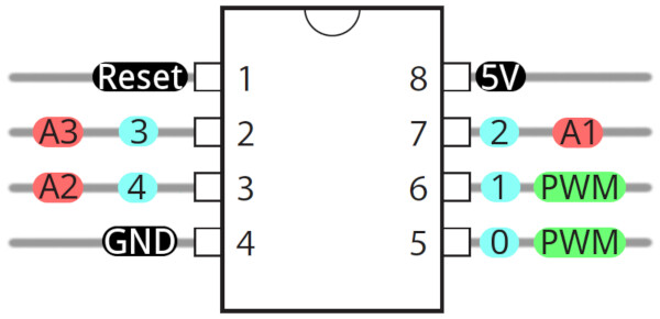
For doing that I'm using this ATtiny45 pinout reference, as both boards I'm designing have this microcontroller.
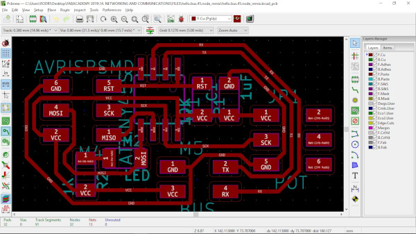
I designed both boards in KiCAD.
This is the bridge board:
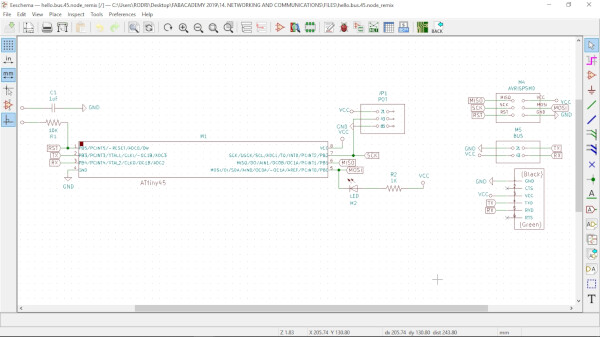
And this is the node board, I connected the signal of the analog sensor to the pin 7, so according to the pinout reference, I'll be using A1 as the input pin:
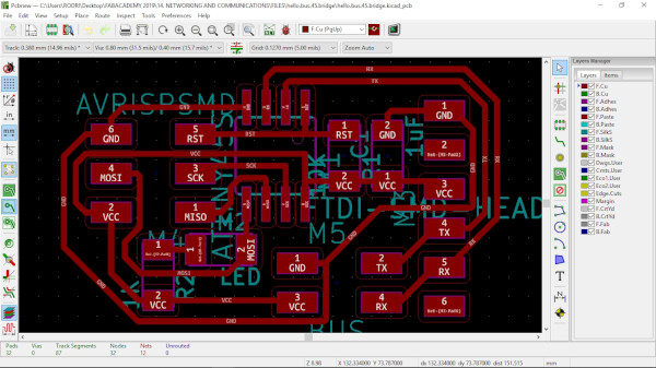
I designed this boards using this design rules:
Clearance: 0.4mm (this is the diamater of the 1/64" mill tool).
Track Width: 0.38mm
I used this parameters to have good spacing between the tracks, and have thick tracks to better solder components.
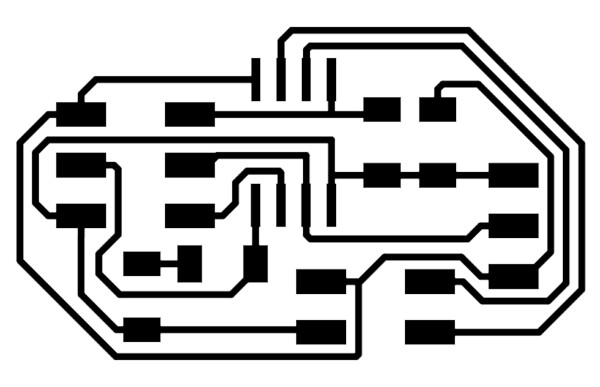
After exporting the SVG from KiCAD, I draw the outline/profile of the boards in Inkscape and exported the profile and traces png files.
These are the bridge board traces and profile files:
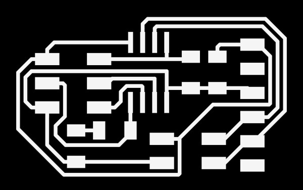

And these are the node board traces and profile files, notice that the colors are inverted, this doesn't matter because FabModules have an option to invert them if necessar:

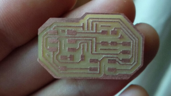
I then created the .rml files in FabModules and milled the boards.
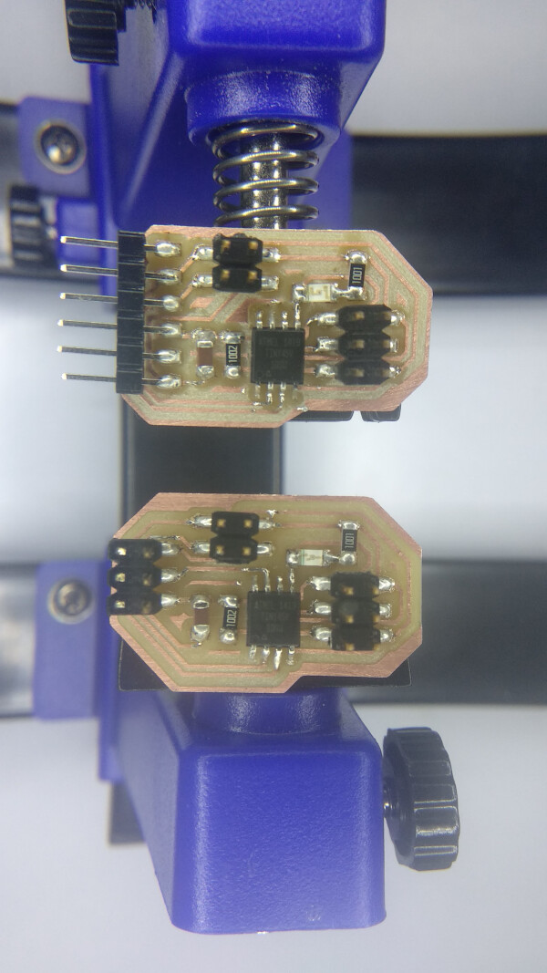
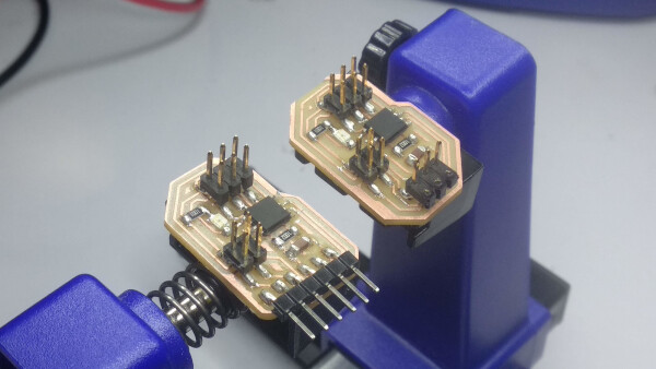
I then selected all the components and organize them to solder them.
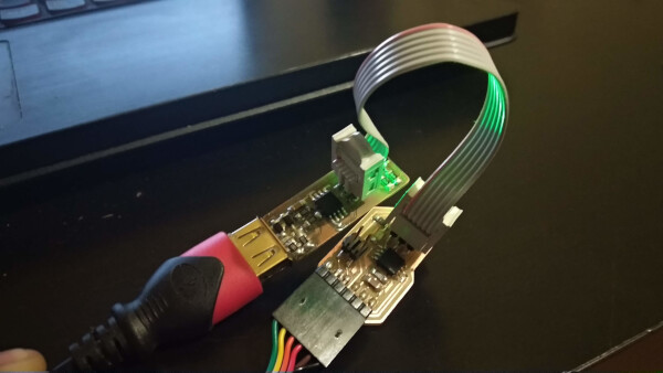
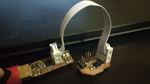
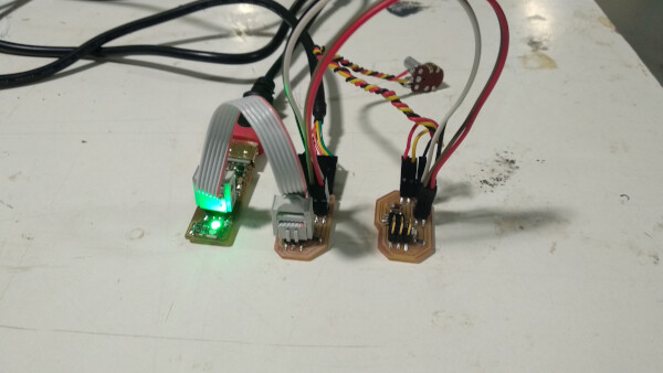
These are the boards after solder all the components:
I then tried to burn the bootloader at the bridge board connecting the FabISP, but I was having troubles doing it. I realized the problem was that I didn't connect a power supply to the bridge board.
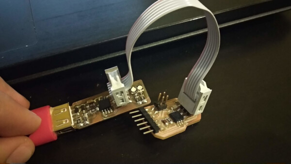
So I connected the FTDI to give it current to the board. Now the led of the FabISP turned on.
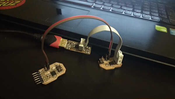
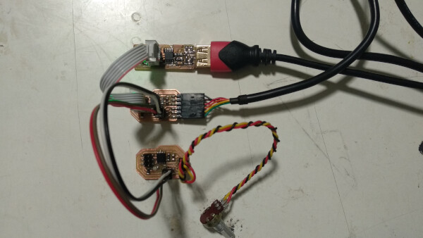
After this connection I succesfully burned the bootloader. I proceed to do the same thing to the node board, but as this board don't have an FTDI, I had to connect it through VCC and GND to the bridge board, and the bridge board to FTDI, this way the FTDI is supplying the bridge board, and the bridge board is supplying the node board. All this was just to give the node board current to burn the bootloader.
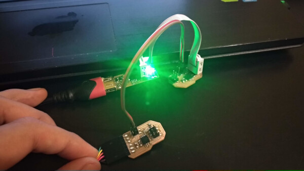
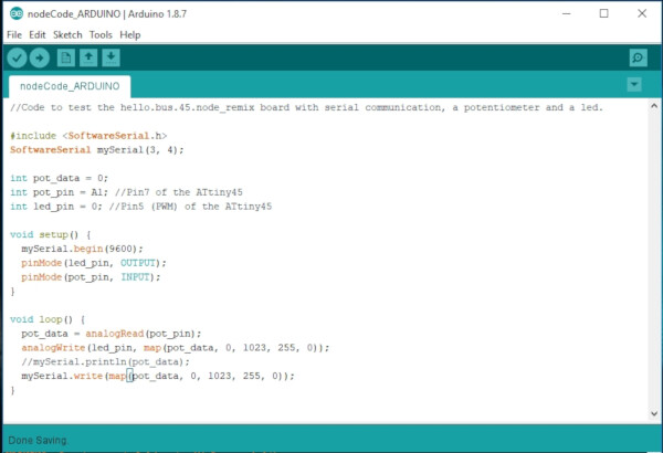
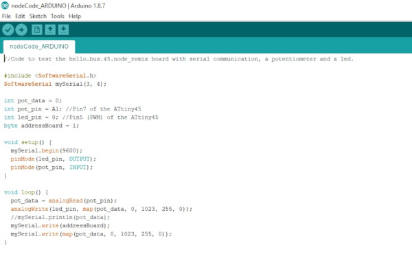
After this, I uploaded a test to the node board, to control the led using the potentiometer and PWM.
I then added that the node board send the potentiometer value through serial.
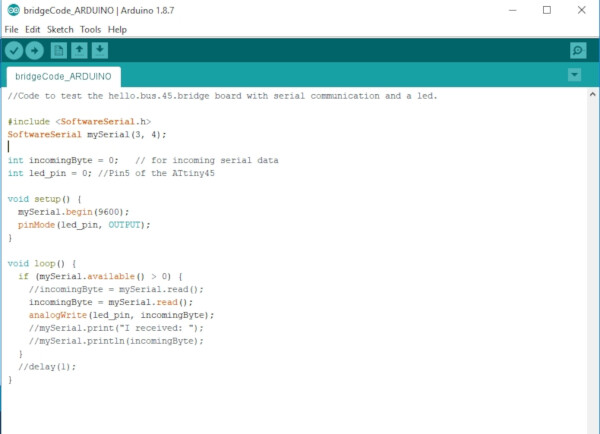
I then connected the TX of the node board to the RX of the bridge board, and the RX of the node board to the TX of the bridge board. I uploaded a code to print what the bridge board is recieving through serial.
There was times where I couldn't upload code to the node board. The reason was that there is serial communication between the node and the bridge boards. The solution is to disconnect the TX and RX wires from the node, upload the code, and then reconnect them. Sometimes I had to turn a little bit the potentiometer to upload a code to the node board.
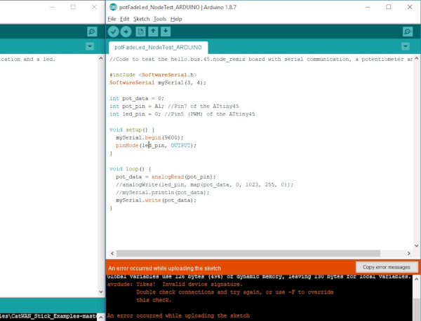
I changed the mySerial.print() function to mySerial.write(). That solved the problem of communication between the two boards, as I was now receiving the data of the potentiometer. To make it work I had to send the mapped value through serial from the node board, and use it in the bridge board to the analogWriite function of the led to make it fade as the potentiometer is turning.
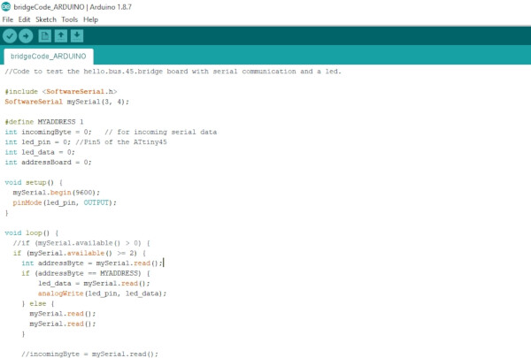
Update: Addressing on code
I added a little part for the codes of the bridge and node, to make it address and specific board. In this case as I'm using only one interaction between boards, it's specified as 1. but if I want to expan the interaction between more boards, I would need just to change the address of the board on this new code.
Files
- Bridge board (KiCAD project)
- Bridge board traces .png
- Bridge board profile .png
- Node board (KiCAD project)
- Node board traces .png
- Node board profile .png
- Bridge Final Code .ino (Arduino)
- Node Final Code .ino (Arduino)
- Node board Test Potentiometer code .ino (Arduino)
- Node board Led Fade code .ino (Arduino)
- Bridge board Serial Communication code .ino (Arduino)
- Bridge and Node board Serial Communication code .ino (Arduino)
Group Assignment
To see this weeks group assignment click here.