7. Electronics design
This week we had a group assignment of using the test equipment in our lab to observe the operations of a microcontroller circuit board, and we had the individual assignment of redrawing the “Echo Hello-World Board”, adding a button and an LED, as well as making and testing it.
Group Assignment
I started this week out by sitting down together with my group and working on the group assignment. We used an Oscilloscope to observe an Arduino uno 3 that was just running a simple blink program.

I had never even touched an oscilloscope before this, so I figured the best thing to do was take a step back and start slow. We used this video from Sparkfun to help us get started. The video had a lot of helpful tips for getting started, so much so that we actually didn’t need anything else to do this other than a couple tips from Mr. Rudolph. We followed the steps outlined in the video for getting the machine set up.
First we turned on the machine and let it load itself up, then we checked that the probe was in channel one, and set the coupling to DC. Then, we made sure the probe was set to “10x” and opened up the trigger settings.
Under the trigger settings, we made sure that “Type” was set to edge, and that “Slope” was set to upedge. Our scope came with a built in frequency generator of 1 khz in square waves for the sake of tuning the probe correctly. We connected the probe to the frequency generator and the waves popped up on the screen. At first, they had a slightly angled edge which meant the probe was not tuned correctly, so we used a small screwdriver to turn the tuning screw on the probe until we had the squarest waves we could get.
After we were sure it was tuned correctly, we then went ahead and got out a microcontroller to observe. We used an Arduino Uno 3 with a simple blink program on it that blinked the onboard LED on and off at intervals of one second each. To actually do the testing and observation, we grabbed a few jumper wires and used those to plug the probe into the “P13” and “Gnd” headers. After it was plugged in, we ran the blink program and watched as the square waves on the oscilloscope changed from high to low along with the blinking of the led. This was pretty cool to see because in the past when I saw, “set pin 13 HIGH” in the code, I never really knew what it meant, I just assumed that HIGH and LOW were the same as on and off, but now that I have seen it on the oscilloscope I see that it’s actually literally changing the wave along with the blink of the LED which was really neat.
Individual Assignment
My individual assignment this week was to redraw the echo hello world board and add a button as well as an LED to it. To complete this, I will be using the Autodesk Eagle software.
To get started in eagle, the very first thing I did was download the Fablab library for Eagle from Github, which you can find here. After opening it up there, I viewed the raw version by clicking here.
Then I copied all of the text and opened it up in notepad.
After opening it in notepad, I saved it all as one file and dropped that into the libraries folder for eagle in my files.
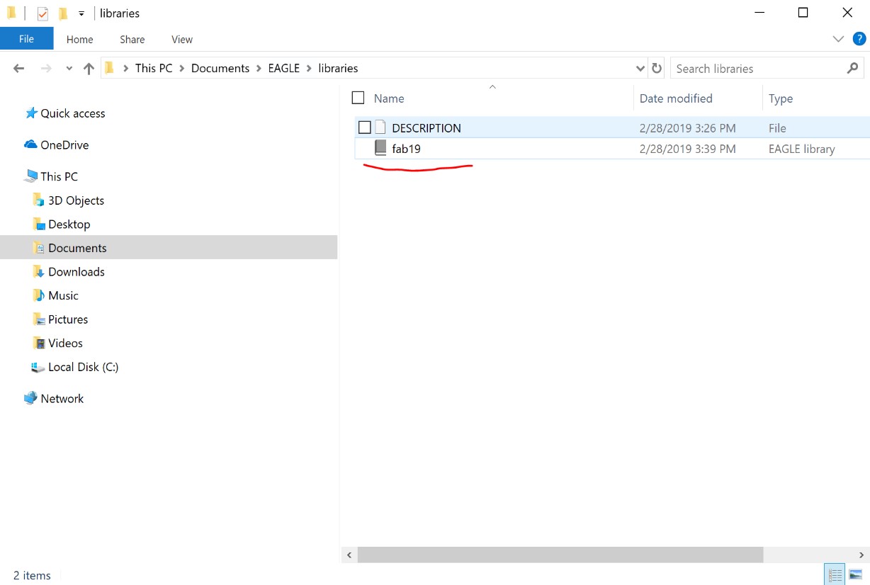
Once the file was where it needed to be, I restarted Eagle and opened up my libraries to find that the Fab library was now there.
I then created a new project called “Hello_World”.
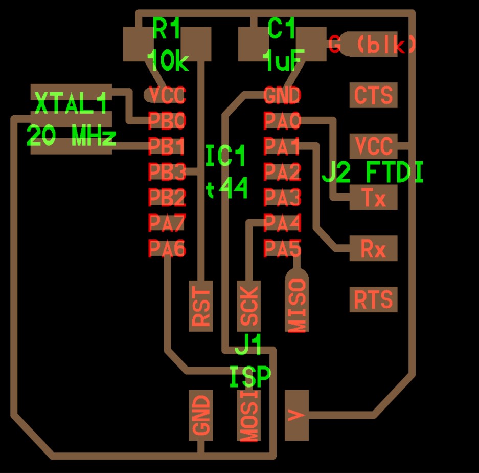
At this point, I started to feel like I was jumping in the deep end. I spent some time looking around to try and find what parts to use, or really just what the echo hello world board was. I also needed to learn how to work with schematics in eagle, luckily I was able to find this tutorial on sparkfun that helped me get started. I also found the schematic for the original board under the embedded programming week notes.
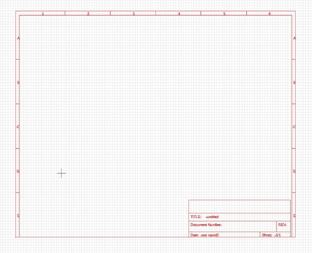
I read through the sparkfun tutorial and started getting the hang of things after a while. I added a frame for reference that looks like this.
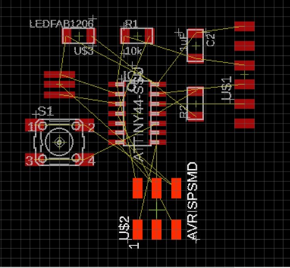
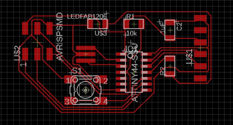
After a while of searching through the libraries and trying to find the correct version of all of the different parts, I had everything I would needed placed down on my schematic.
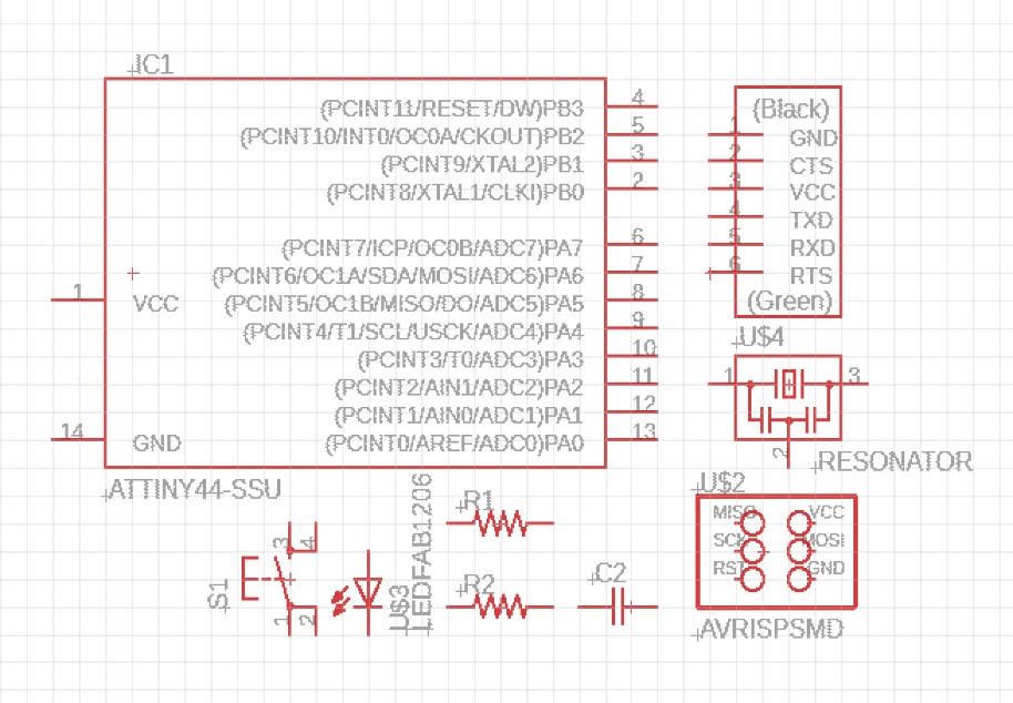
Once I had everything placed down, I then began trying to connect all of my parts together like a proper schematic.
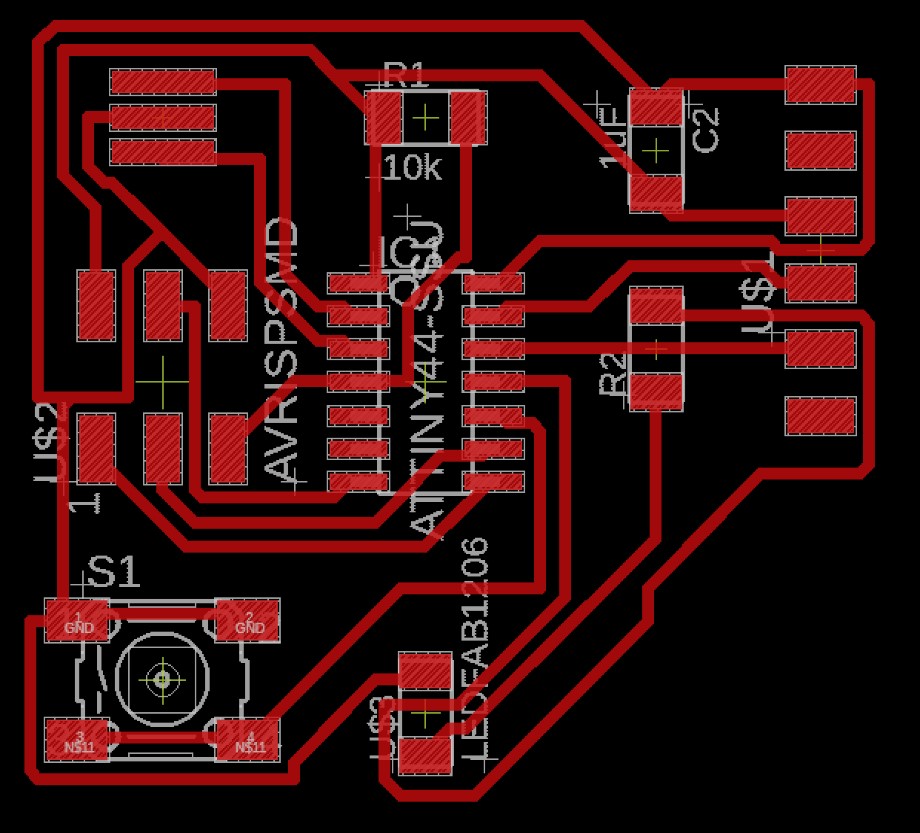
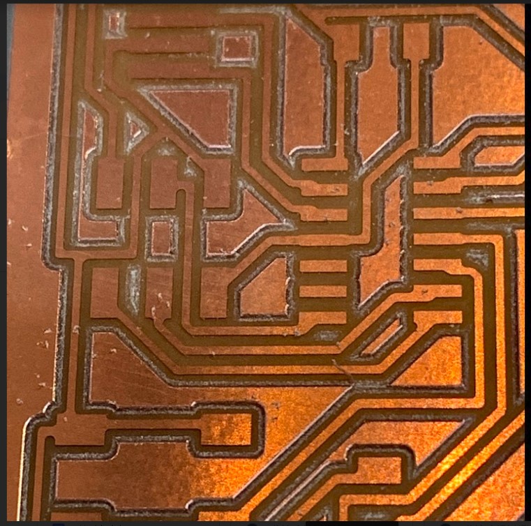
It ended up taking me an excessively long amount of time to get the schematic drawn out, and it honestly looks like quite the rats nest, but things should be connected in the right places now.
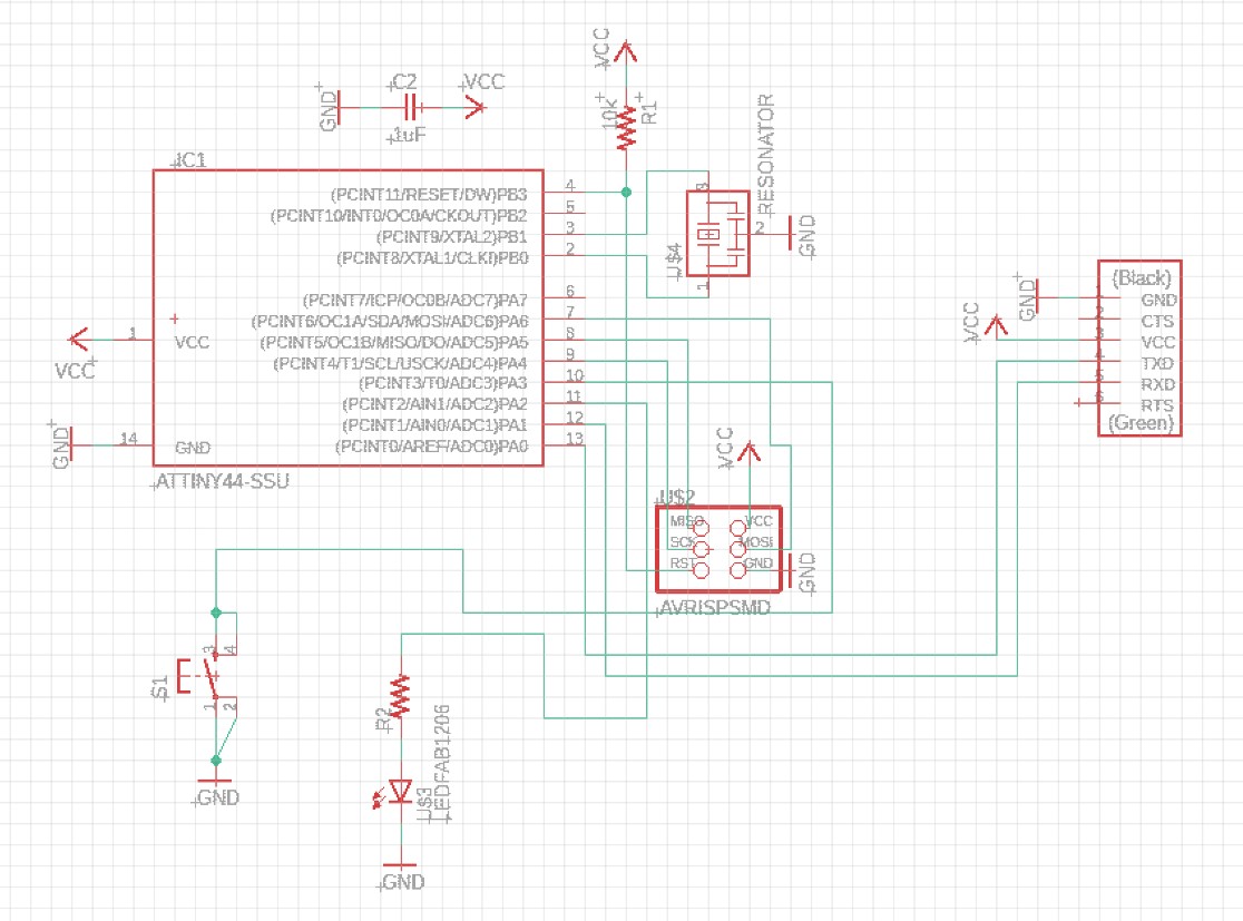
Once I had the schematic created, I went on to the second part of the Sparkfun eagle tutorial. Under the file dropdown tab, I hit “switch to board” and was taken to this window.
This next part was pretty fun to work through. I did try to do some self routing for a bit, but I could never seem to get it to come together, so for the sake of time I ended up just using the auto router. There was one very important step before using the autorouter, though, and that was to change my design rules.
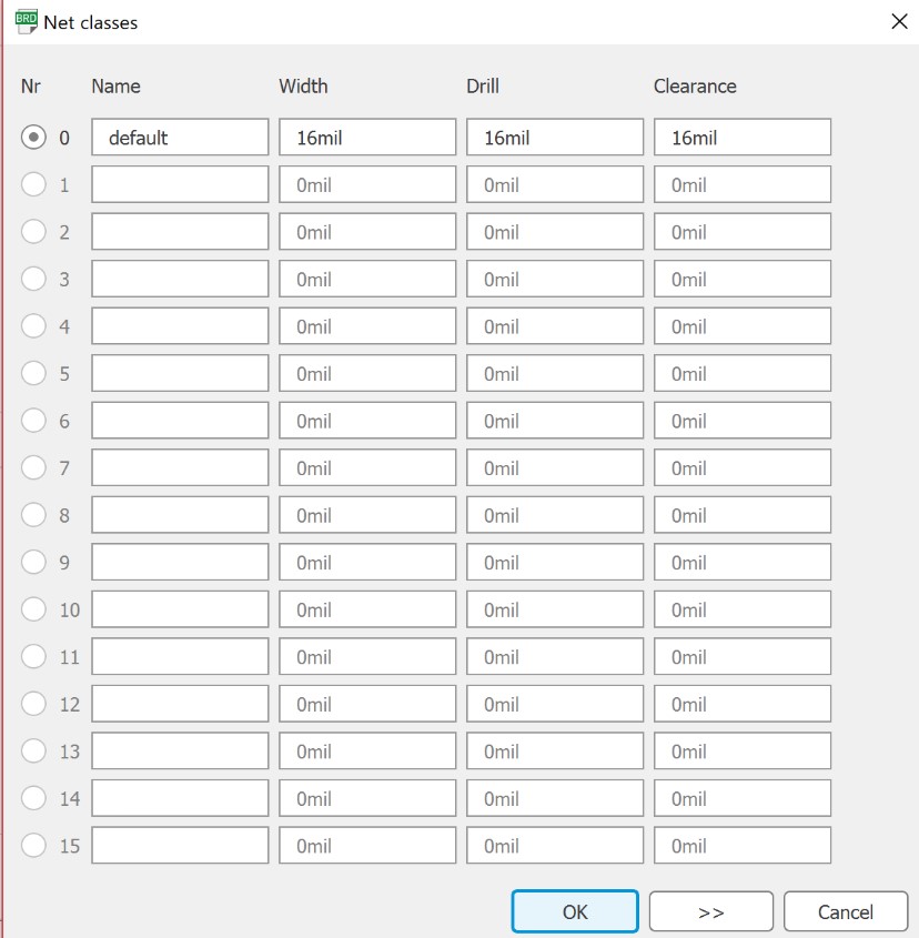
The bit that we are using to mill will be 1/64th of an inch wide, so if there are any gaps between the traces that are less than that in my design, then they just won’t get cut out at all. I’ve read quite a few stories from past students pages and have heard quite a bit about how aggravating this can be from people in in my own lab, so I figured it would be best to save myself the trouble and get that straightened out right away.
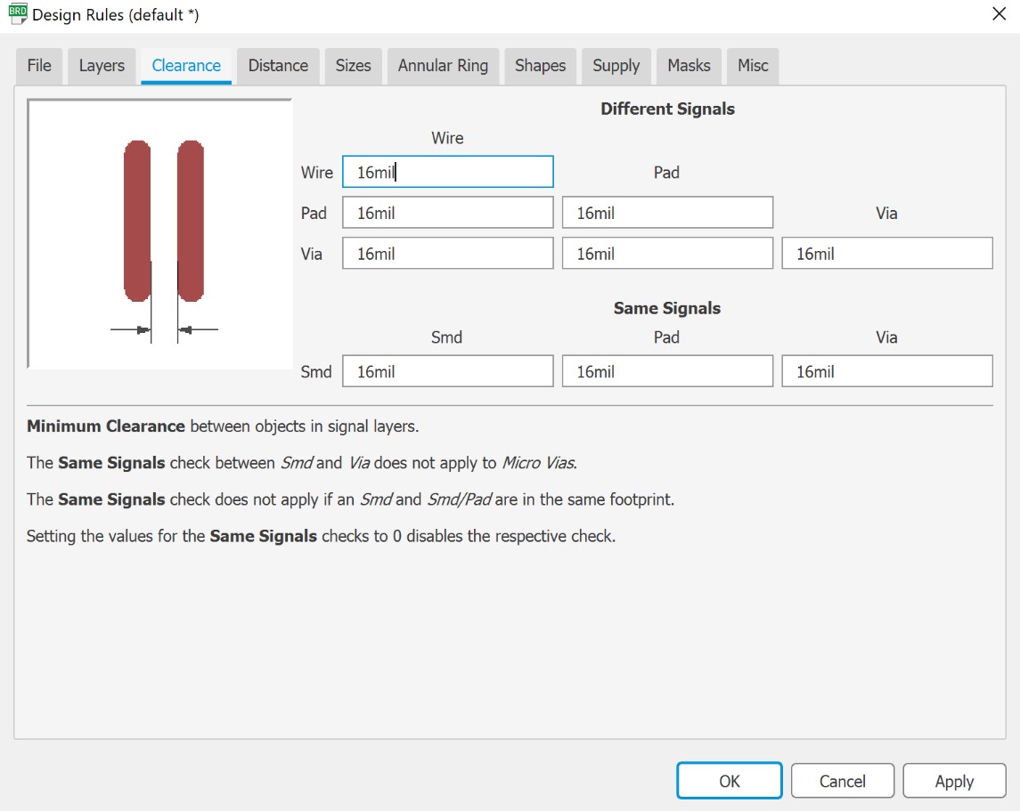
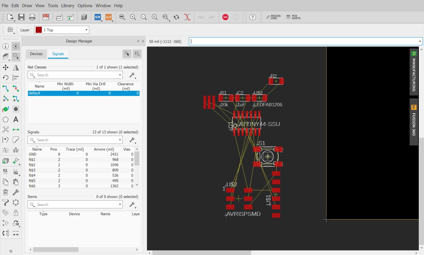
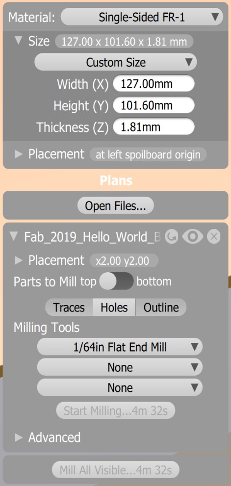
I set the minimum width between everything to be 16mil, or 16 thousandths of an inch, because that’s a bit larger than the width of the bit itself. Once that was set, I arranged my parts in what seemed to be an efficient layout, then I opened up the auto router.
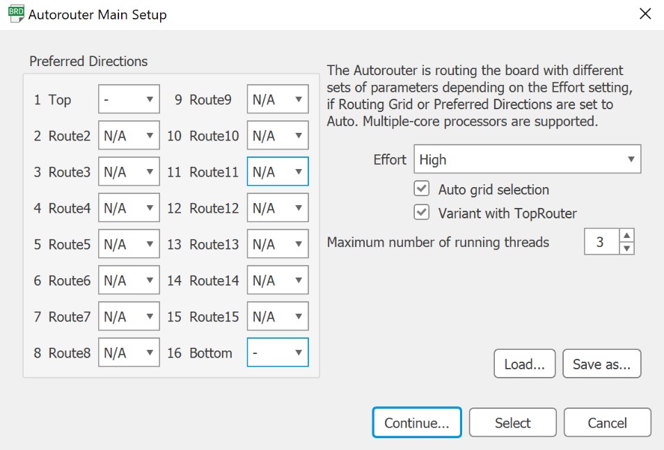
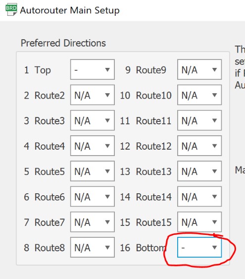
When we mill things out at first, we will only be using a one sided PCB board. This means that I won’t be able to use any vias in my design, which is fine, but it also means that I need to tell the autorouter not to use them either. I had to change the last layer option to “N/A” so that it wouldn’t rout anything underneath the board.
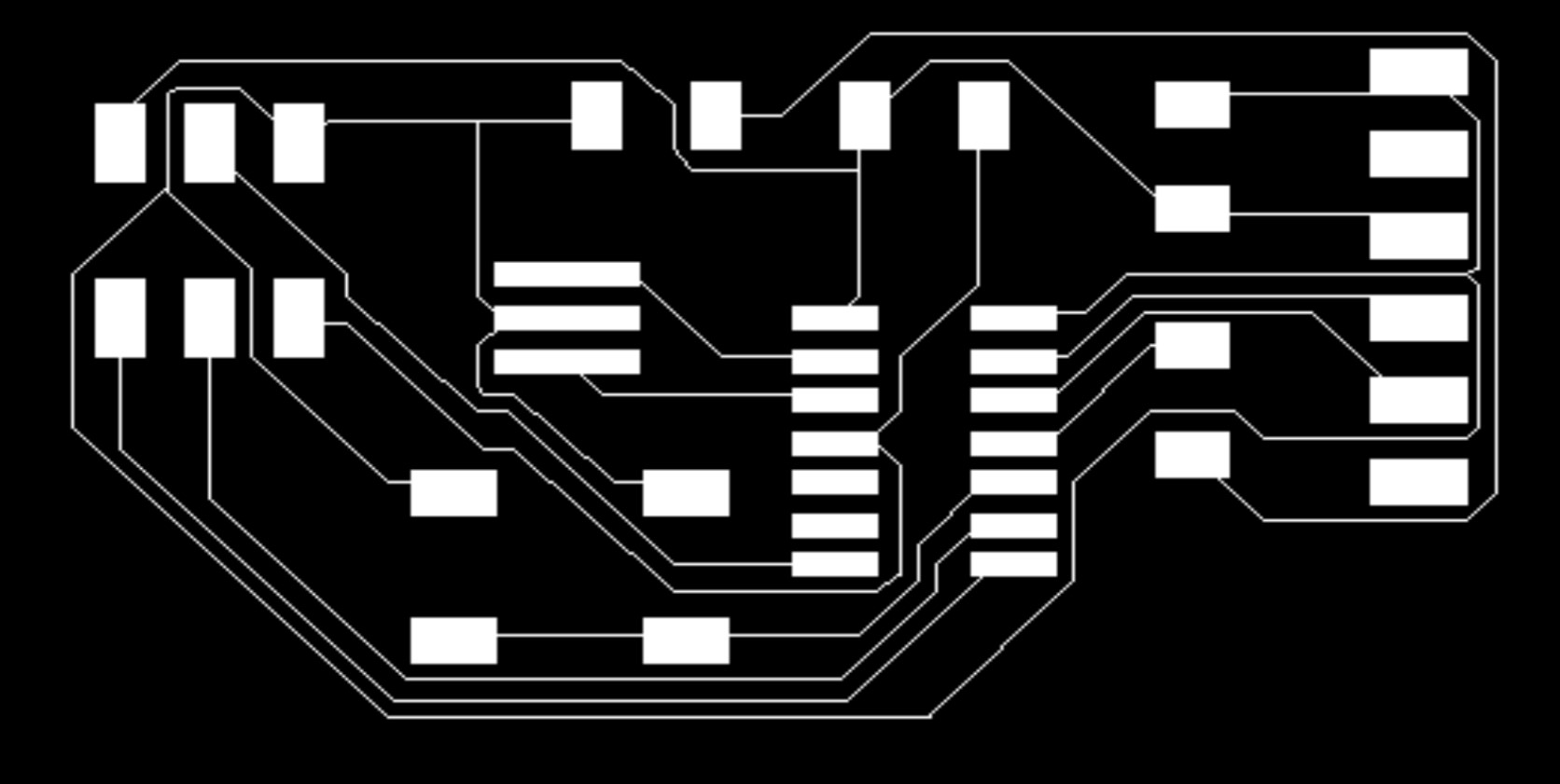
Once that was set as well, I ran the autorouter and watched it work itself through tons of possible pathways until finally settling on the right one.
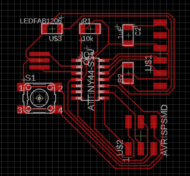
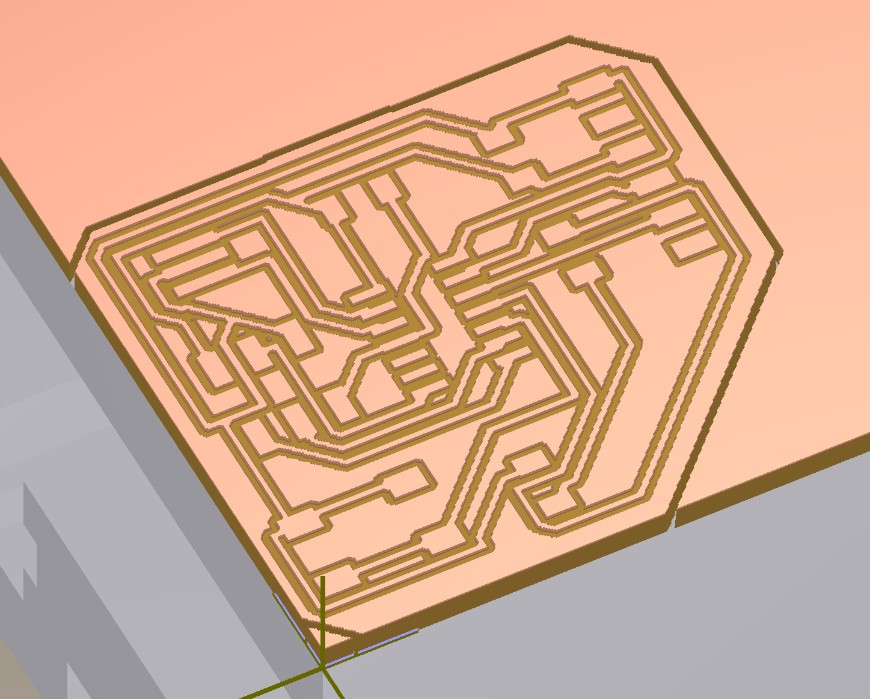
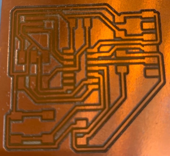
This was successful, but I wanted to have a design with a bit more character to it, one that wasn’t just a square like so many others. Luckily this wasn’t a hard thing to do, all I actually did was move the ISP header to the back of the board rather than the side, giving it a more rectangular shape similar to the original programmers we made before.

Then I ran the autorouter again and settled on this layout for the parts.
At this point, I had everything laid out correctly and I was ready to start milling, so I looked at Mary Fabian’s site to see what I should do next to get it over to fab modules, and then to bantam.
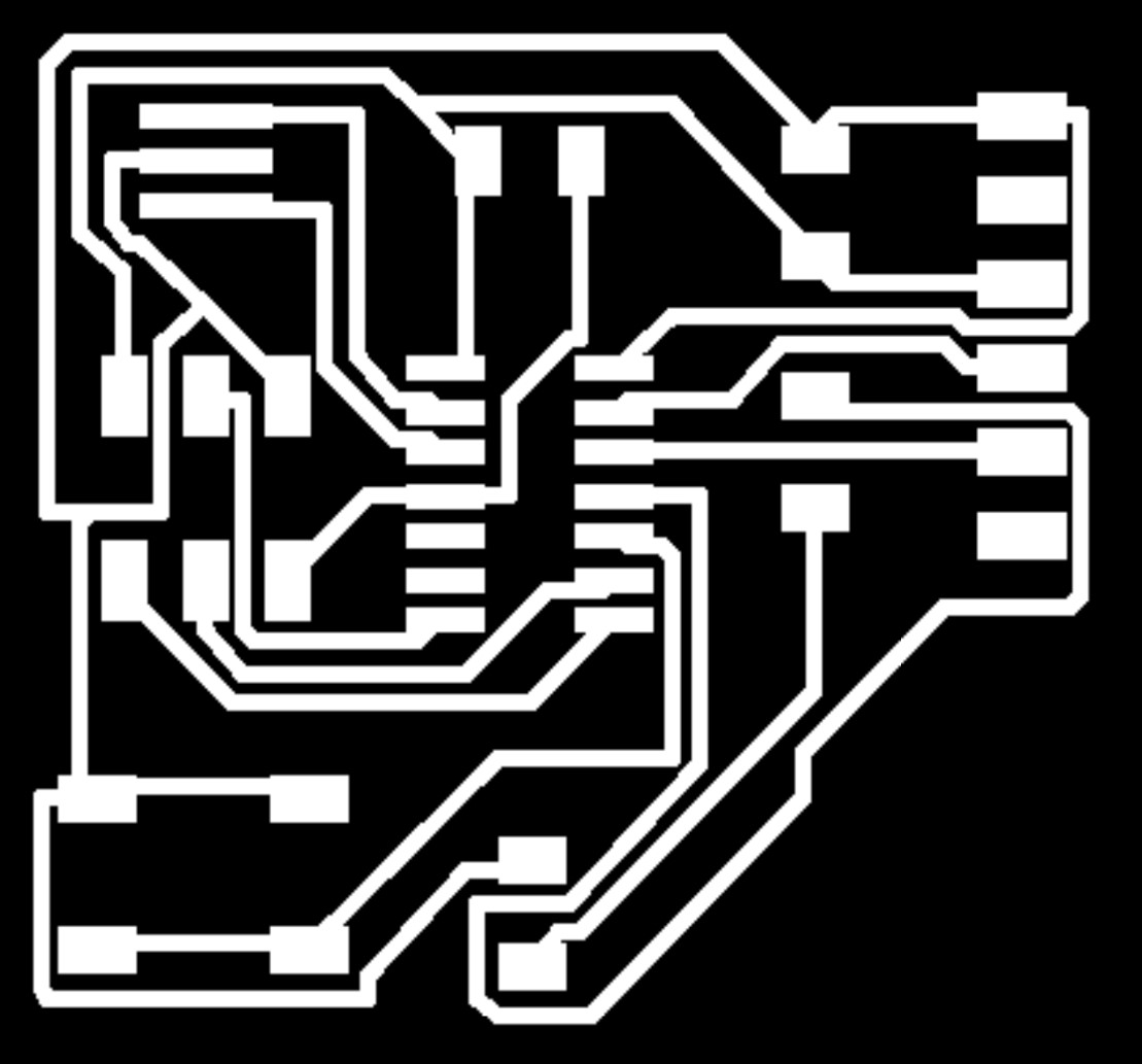
She suggested turning off all of the layers except for the traces, and then exporting the image as a png file in monochrome so that the traces could be read by bantam. I’m a little concerned that these trace widths will be too small to work with, but at a certain point you just have to see for yourself.
I retract my previous statement. After looking through a few more sites from past students as examples, I’m beginning to realize that almost no one else ever used traces as tiny as mine are. This leads me to believe that it probably wouldn’t work out well to have traces that small because it would be super easy to accidentally tear one up. I went back to the drawing board.
I now had to change the auto routers settings so that it would set the trace width a bit wider. To do so, all I did was go under the net classes and change the width, drill, and clearance to 16mil.
I ran the autorouter again and kept on getting into issues with my placement, so I finagled the parts around some more until they were finally in a layout that would work.
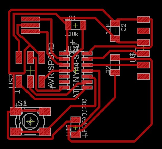
Now I just wanted to clean up some of the traces and make them more compact. This ended up only being one trace, though. Nevertheless, I optimized it a bit more, and after that I ran another ratsnest check and a design rule check, both of which came up clear with no errors.
Next, I did the same thing as before to turn it into a black and white PNG.
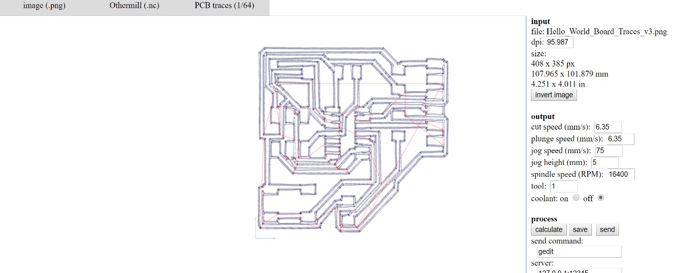
Once I had the PNG file ready, I got it pulled up in Fab Modules to turn it into useable toolpaths for the milling machine. I got it made into a .nc file with 1/64th inch traces and then sent it over to bantam.
When I pulled the file up in Bantam, though, it didn’t look quite right.
The file would have been far too large to cut, and the traces all looked sub par. I’m gonna go back over everything and see what to do next.
After getting a tip from Mr Rudolph, I realized I could just pull the eagle file up in bantam directly rather than having to go through Fab Modules. I did this right away and the file came up looking much nicer.
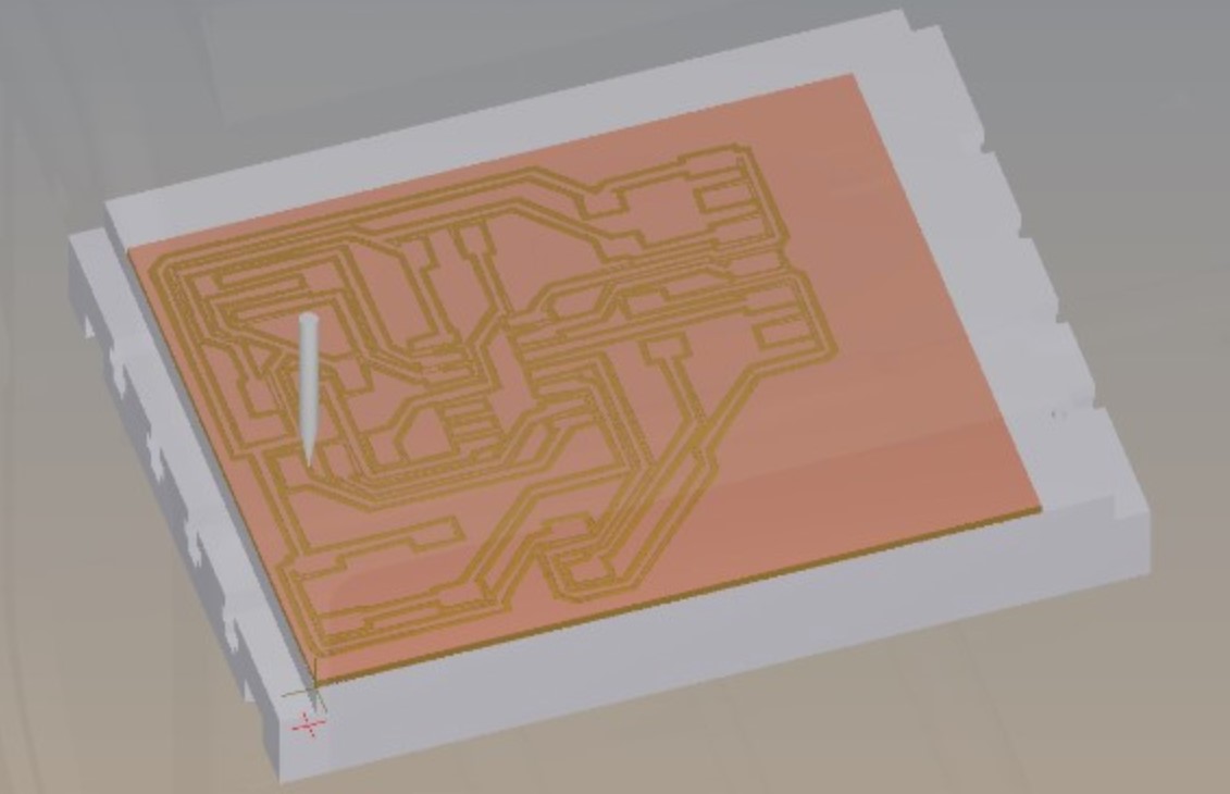
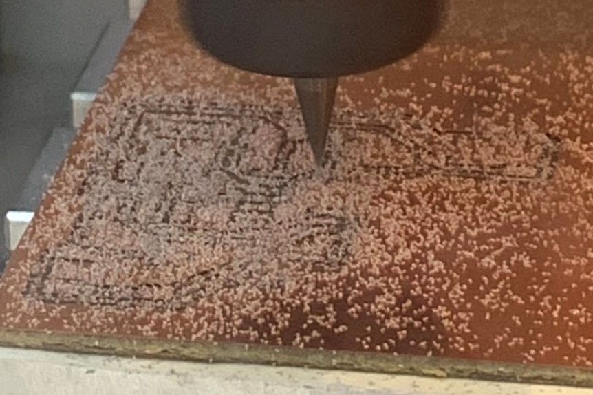
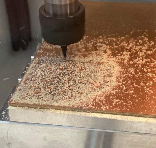
Once I had the correct file in Bantam, I homed the x, y, and z axises, set my material thickness, and opted to use a 1/64th inch bit to do the first pass on the traces.
I got the PCB secured down onto the bed with double sided tape, and then I started the cut which went smoothly.
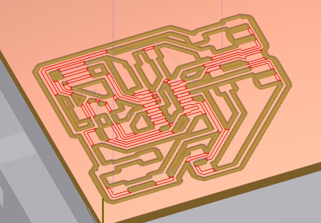
Then, I wanted to go through the same traces again with the 1/32nd inch bit this time to clear out some of the excess copper where I didnt need it on my board. Thankfully, the bantam software knows not to run the bit through places that would mess up the already established traces, meaning there is nothing to worry about when doing this. Anywhere that you see outlined in red is where the tool will not pass through like it usually would with a 1/64th inch bit.
The cut itself went smoothly yet again, but it didn’t look like the bit had gone quite far enough down into the copper.
I ran it again and moved the cut depth down by .05 mm, which seems to have worked a little better.
The last thing I did was run the outline cut, for which I used a 1/32nd inch bit again.
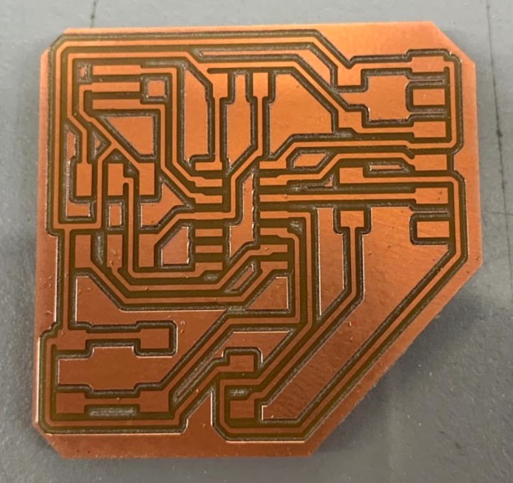
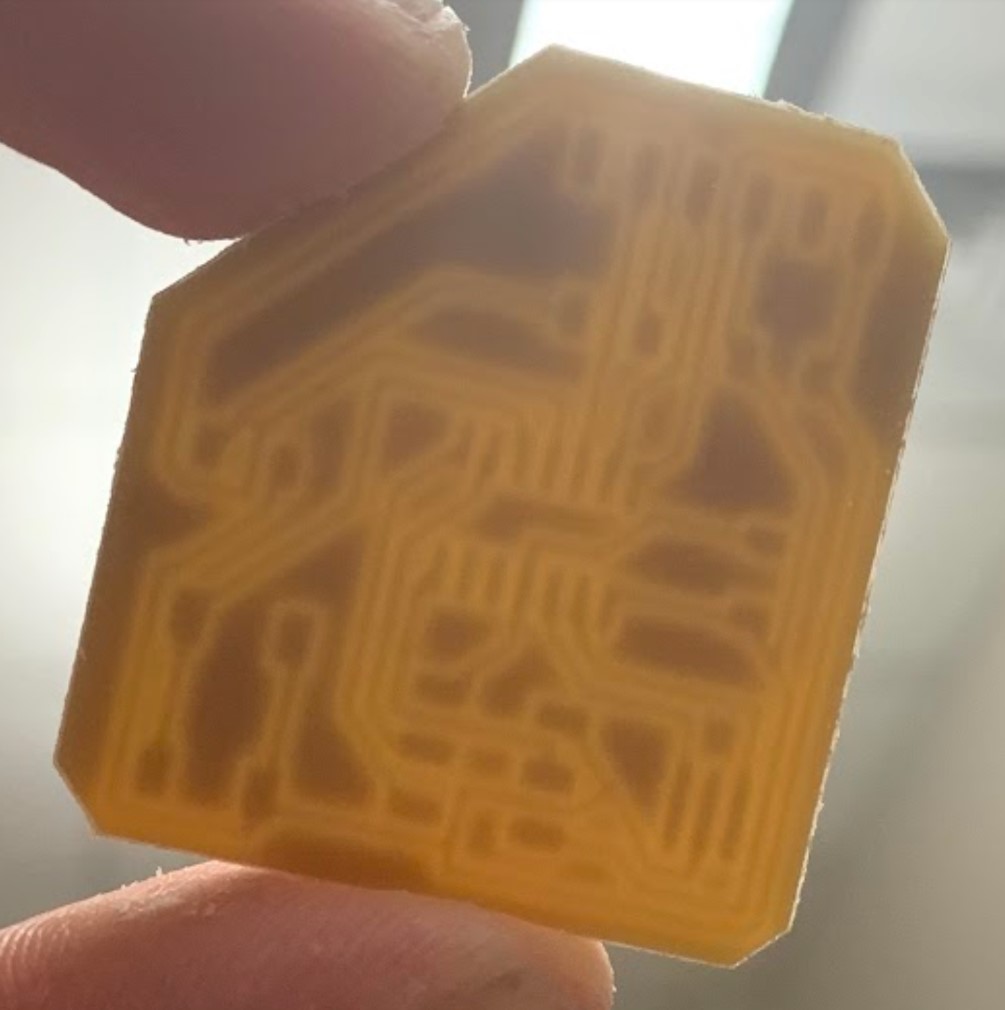
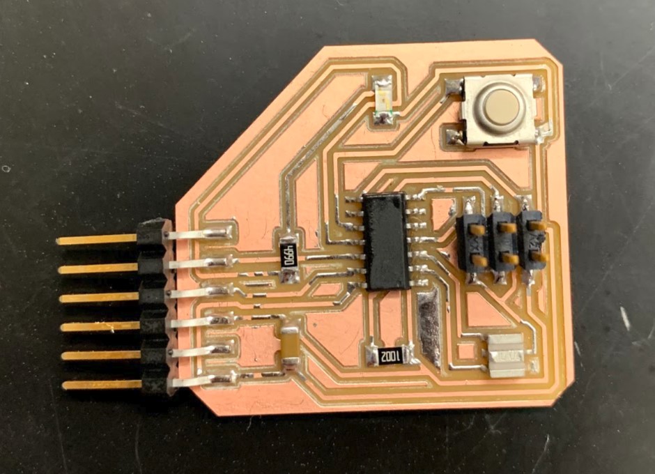
The board came out very nicely, and while I was observing it I noticed something that I thought was cool. If you hold it up to the light, the copper traces stand out very starkly against the pcb background which looks pretty neat.
Soldering
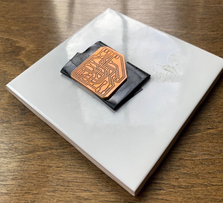
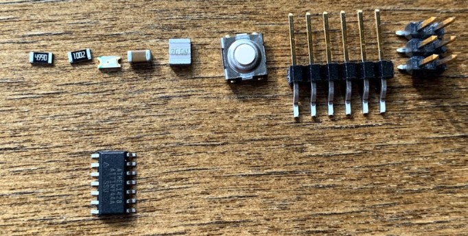
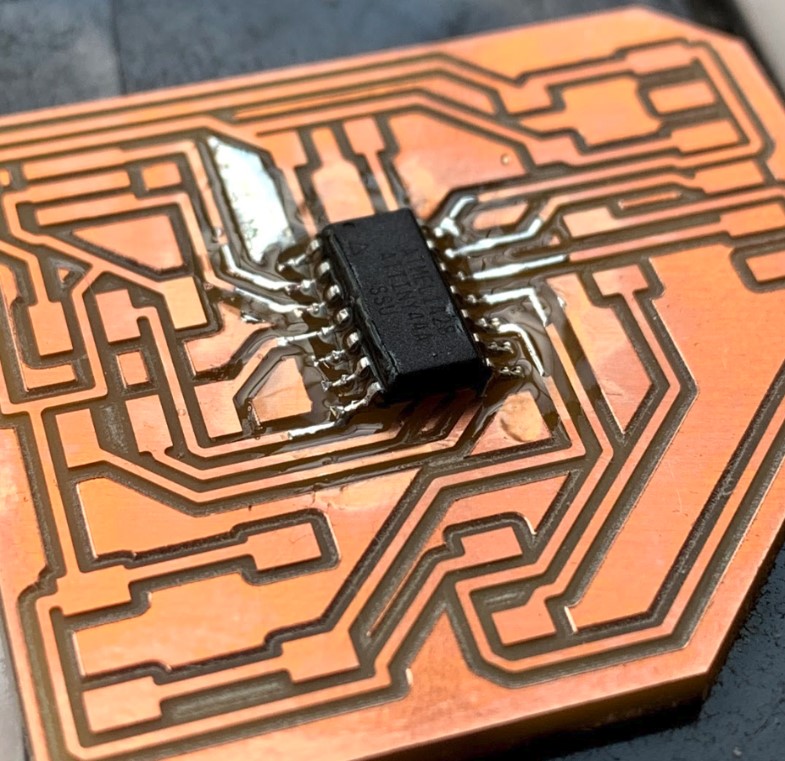
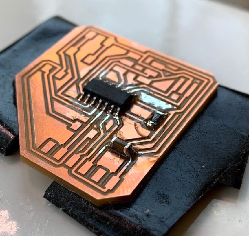
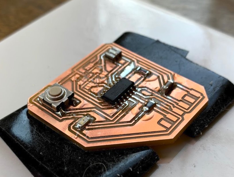
The board had been cut and I had found all of the correct components, so I went ahead and began soldering it. I once again taped my board down to a tile so that it would be secure and wouldn’t move around a bunch when I was working on it.
The soldering itself wasn’t too hard and it only took me about a half hour. Here are some photos that show the progression of my work.
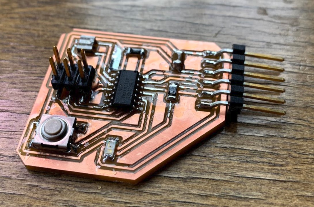
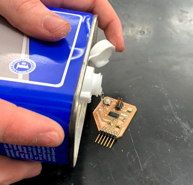
Once I had the board soldered, I wanted to get it cleaned up a bit more. I rinsed it off with water to flush out any particulate that may have built up in the trace cuts, then I used acetone to finish it all up. The water actually isn’t damaging to the board at all as long as there is no moisture still on the board itself when you start to power it.
I then used a brush to help clean it.
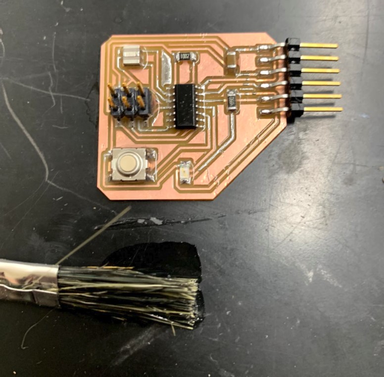
This removed some of the extra material around the board and tidied it up a bit as planned.
Jumping Into the Deep End (AKA programming my board)
If you couldn’t tell by the name of the header above, this was fairly challenging to figure out. This is the first time that I really had no semblance of an idea about what to do, so I hopped on google and started looking at previous sites from last year in an effort to start wrapping my head around what I need to do. I found that a surprising number of people didn’t ever get around to uploading anything onto their board during this assignment, but there were certainly a few people who had done it well. I’ll link below each site that I used to help me further my progress.
From Greg’s site, I found this link that helped me understand how to get going.
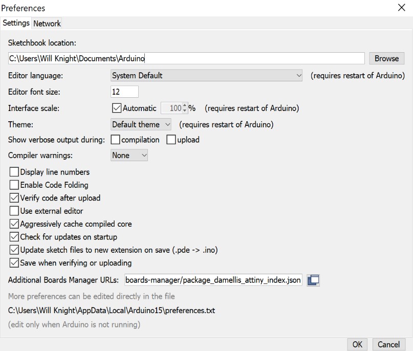
I first started by adding the Attiny44 board into my Arduino software. To do so, I copied the link below and pasted it in under Preferences-Additional board manager URL’s.
https://raw.githubusercontent.com/damellis/attiny/ide-1.6.x-boards-manager/package_damellis_attiny_index.json
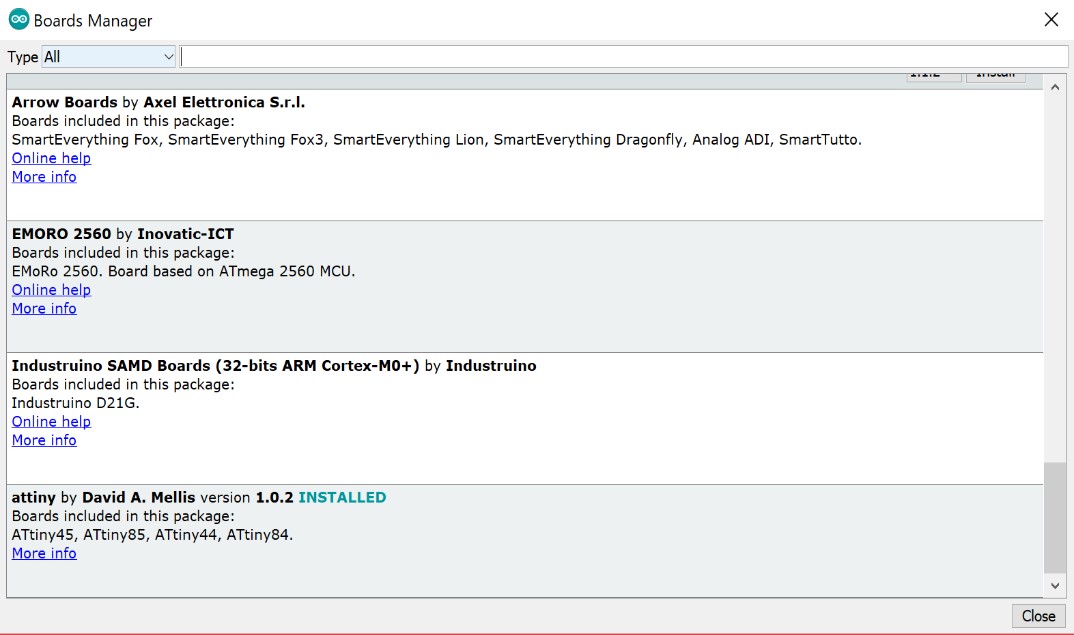
After adding it in there, I went under tools and opened up the boards manager.
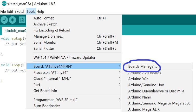
Then I went to the bottom of the list and installed the Attiny board.
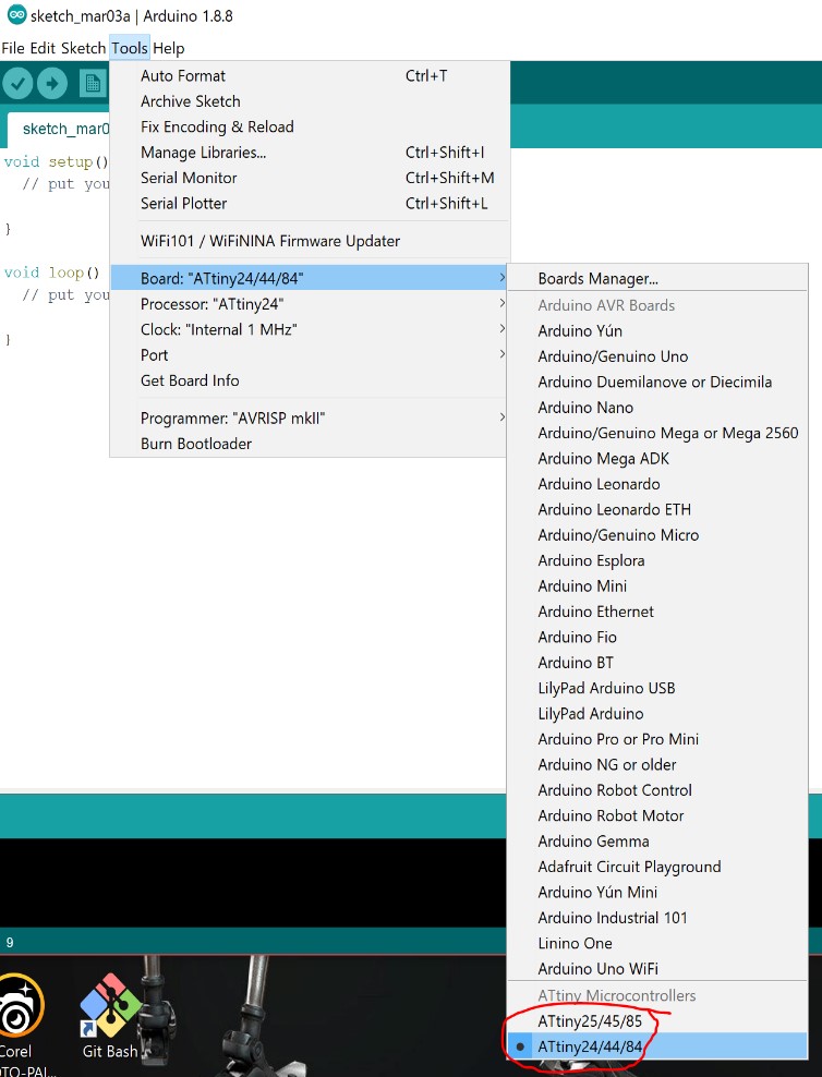
Once I installed it, I could then select the Attiny44 board in Arduino.
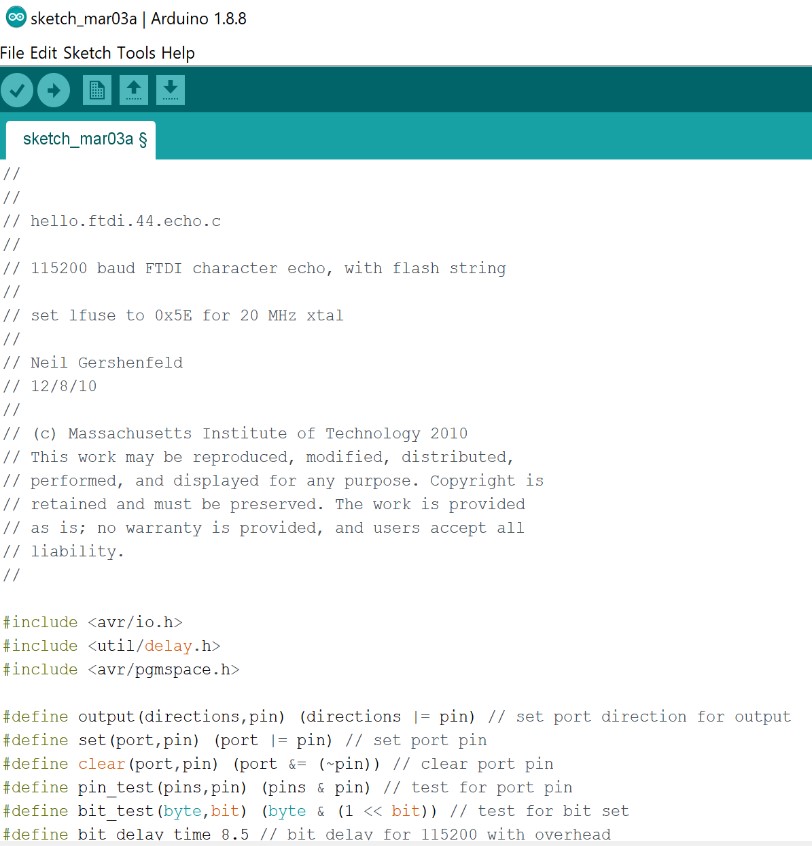
After getting that installed, I stopped using that tutorial and forged ahead on my own because I was starting to see what to do. I got the program itself from the weekly notes that Neil provided and dropped it into arduino.
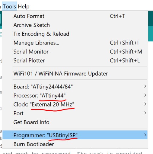
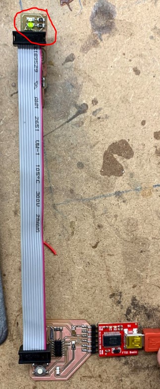
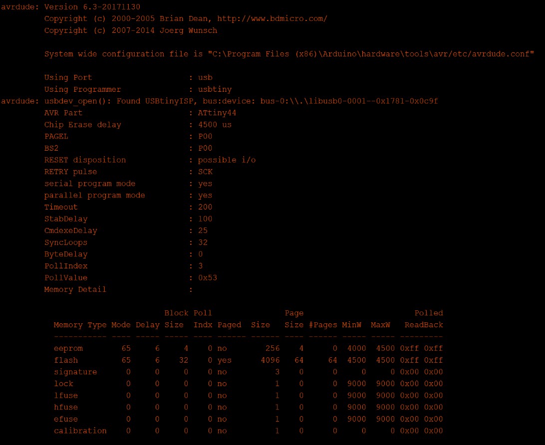
Then, under tools, I made sure the processor was the Attiny44, the clock speed was set to external 20 mhz, and that the programmer was the USBtinyISP. I’ll actually be using the programmer that I made two weeks ago to program this new board that I made yesterday.
I compiled the code in arduino to be sure it would work, which went smoothly.

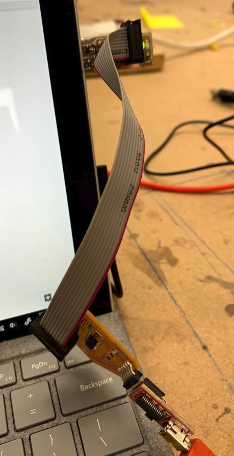
Then, I connected my boards to my computer. When I just powered the hello world board, the led on the USBtinyISP also lit up, which was a good sign.
Once everything was connected correctly, I uploaded the code to my board. Here are the verbose outputs from that.
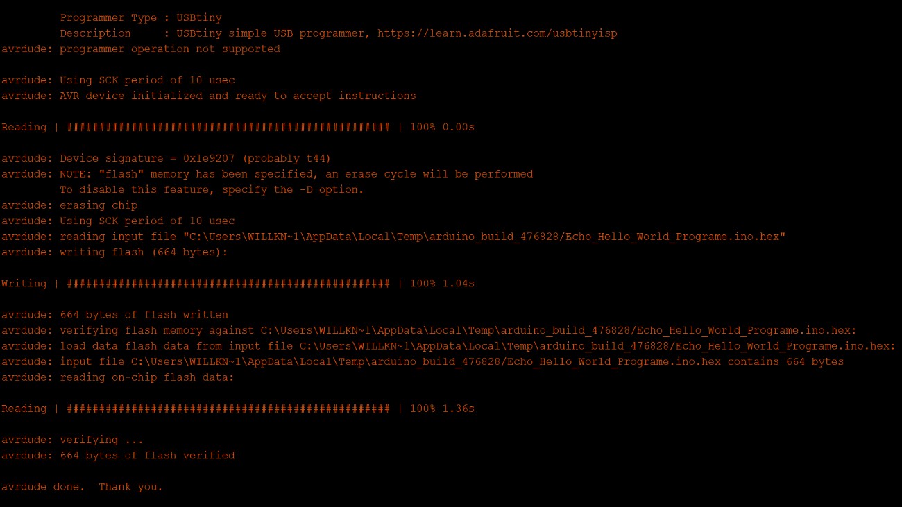
The upload went smoothly, I think it all worked the way it was supposed to, now it’s time to test it out and see.
I selected com 7 in arduino once I plugged in my board, then I opened up the serial monitor and changed the baud to 115200. I typed into the serial monitor and sent it, but all it did was spit back a bunch of gibberish, meaning that I had an issue somewhere in my process.
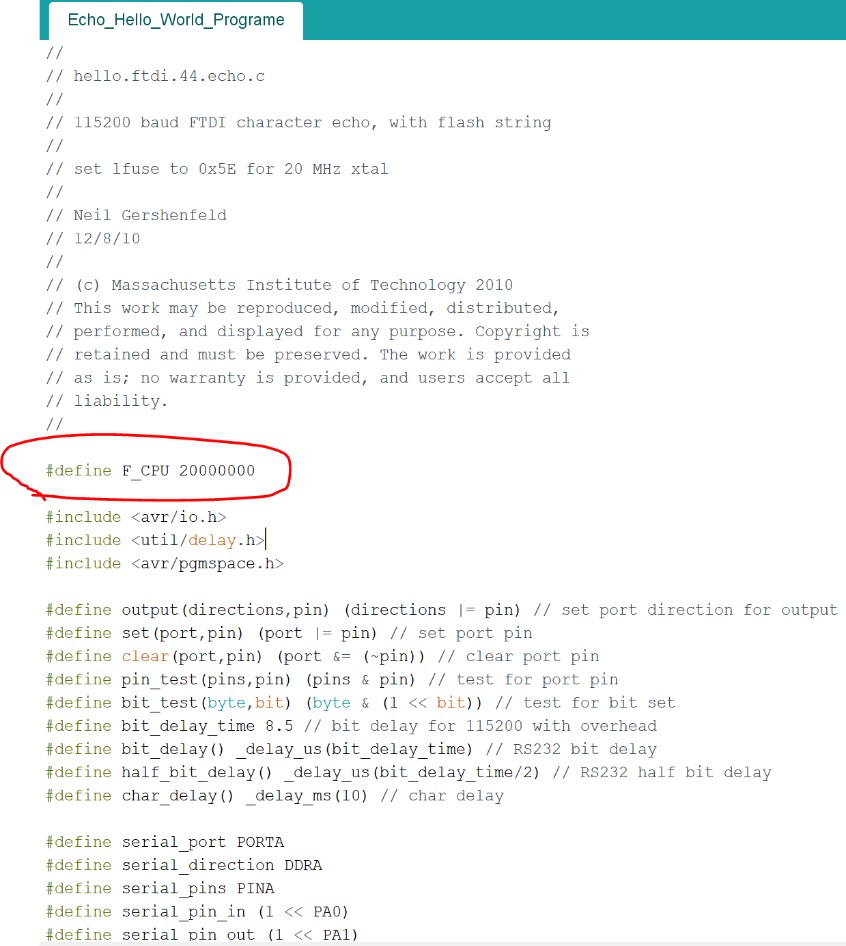
I went back over things with my instructor and he pointed out the one key thing that I was missing. In the program, you have to define the clock speed of the resonator like so.
After fixing this, I went back and tried programming my board again, but once again it wasn’t working. This time, when I tried typing into the command line, I literally got back nothing. I would type a letter, say “h” for example, and press enter, but once I entered it the letter would go away and be replaced with nothing while the serial monitor itself showed nothing as well. This was fairly annoying, but I knew I needed to keep working on it.
At one point, I considered switching over to Atmel studio and programming my board through there, but I was having trouble getting it to recognize my programmer as an actual programmer. I struggled through this for a little longer, and after still no progress I was about ready to call it a day. In a last ditch effort, I went back into arduino and tried looking around a bit more to see if maybe it was just something obvious I had glazed over. I’m lucky that I did this, because otherwise I might have troubled over it for much much longer.
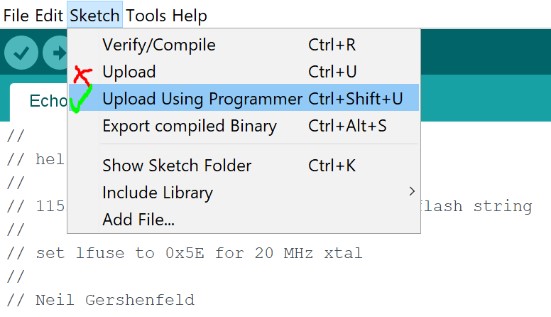
When I was in arduino, I looked under sketch and found that there were actually two options to upload my code. One of them was a basic “Upload” but the other one said “Upload using Programmer”. I’m still not absolutely positive that that is what was causing the issue due to how finicky arduino can be at times, but it fixed my troubles nonetheless.
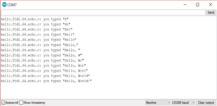
I tried uploading the code using this new option and it appeared to go smoothly yet again, but I was still sceptical after it had seemed fine previously and then ended up failing. I switched over to Com 7, opened up the serial monitor, and sent the letter “h”, expecting it to fail and be unresponsive. To my great excitement, though, it actually worked!! I filled out the message “Hello, World!” and was very excited to see the same message come right back to me.
Here are all of my files from this week.