Let's Go
What is Milling?
It is designed to cut or shape metal using a rotating tool.
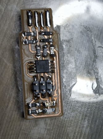
What is PCB Milling
is the process of removing areas of copper from a sheet of printed circuit board material to recreate the circuit according to the design or layout.
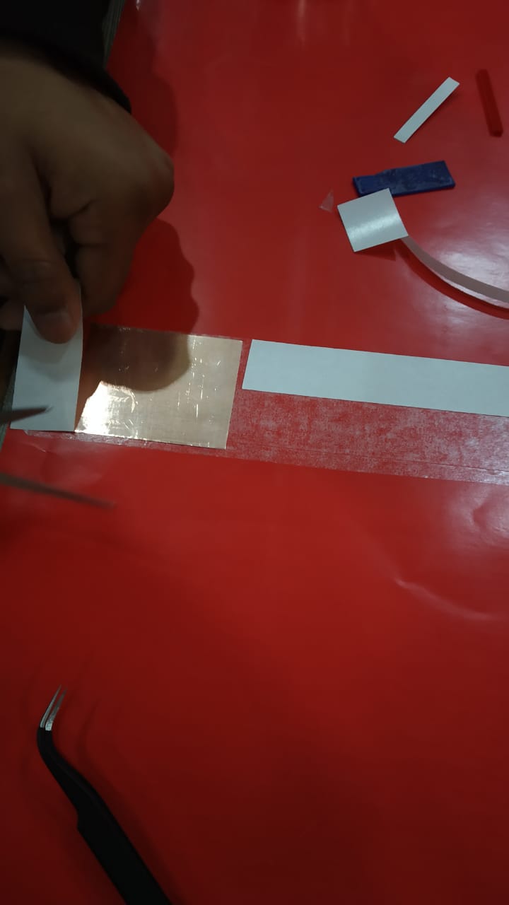
Earlier I've tried Making PCB's by Etching process
In etching we take an Impression of our print on the board by some heat treatment and dip it in FeCl3 solution and the rest copper parts are removed only the imprinted part is left.
But this time I was going to learn a new technique for PCB manufacturing. Although this (milling) method is good for personal use not for commercial use.
First Things First
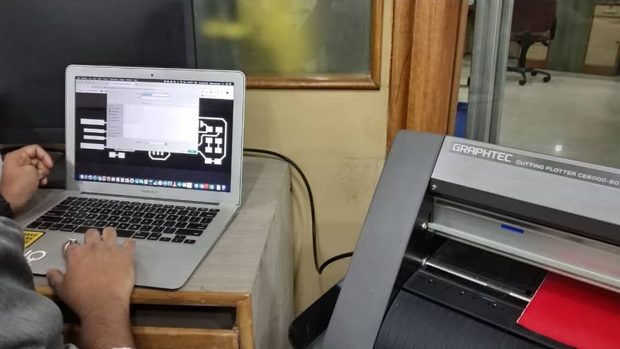
Introduction to Mods-
For the input to the milling machine we have to give it .rml file which is basically composed of G-Codes
G-codes are basically the language that the Milling machine understand it is basically the co-ordinate system x,y,z system.
The work flow is as follows-
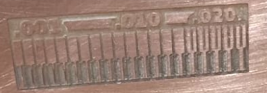
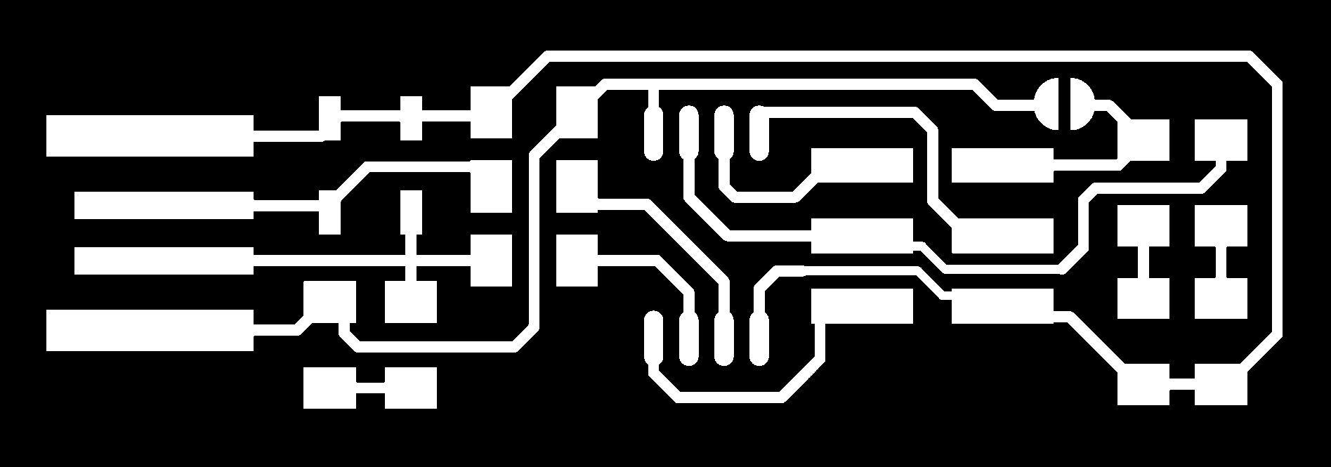
Testing the Milling traces

you can check out the files from this
link.
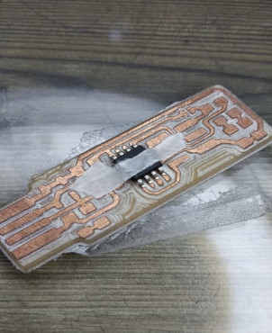
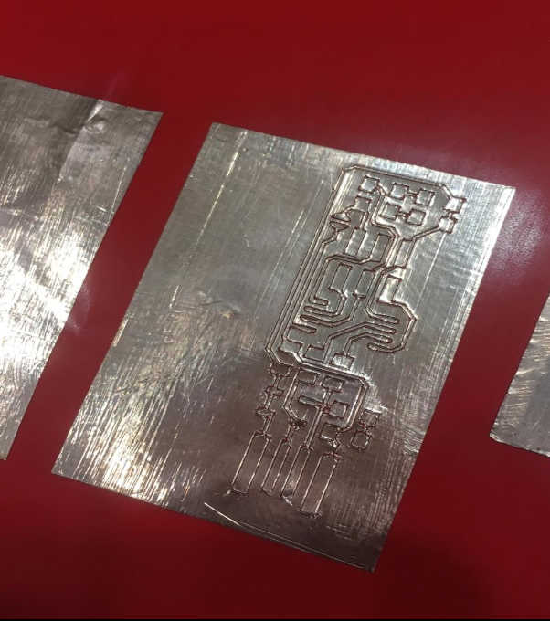
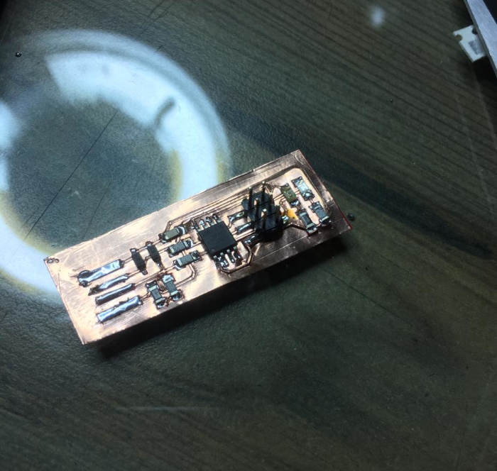
I performed the test using 1/64 endmill and it clearly milled to the last of .001 trace in a good manner.
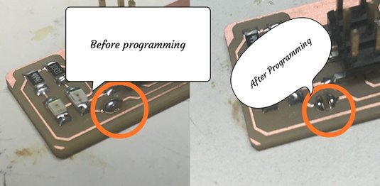
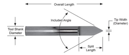
However in making our ISP I used V-Bit because of non availabiltiy of 1/32 endmills and also the pointed edge of 1/64 end mill was blunt somehow fue to some mis-handeling of the bits.
For the group assignment you can go to our group assignment page from this
link.
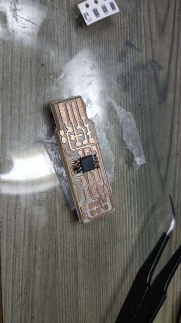
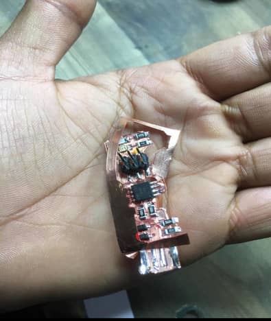
Let's Make the Fab ISP
Step 1-Selecting the Fab-ISP
There are various versiions of Fab-ISP one can choose any one to make I decided to make
Brian's
ISP.
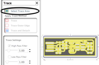
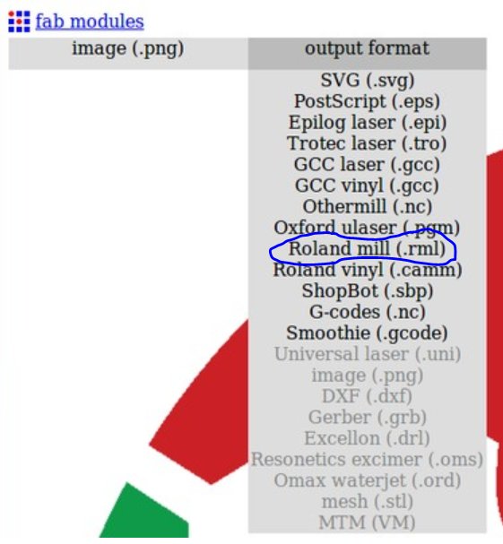
Step 2 - Using Mods
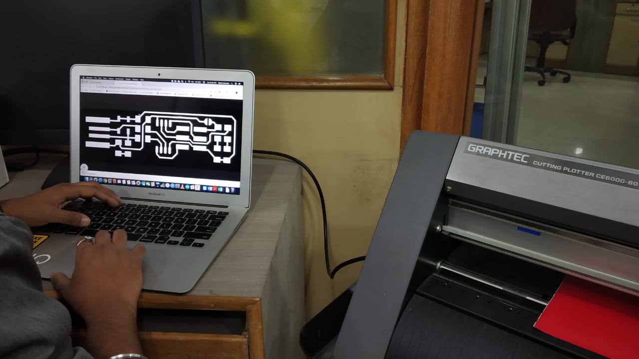
Selecting the output image type, in my case it was .rml.
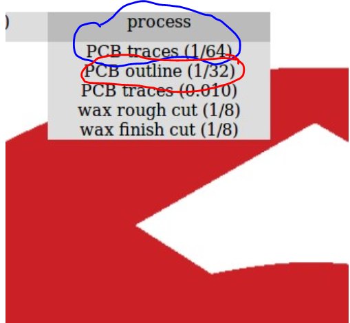
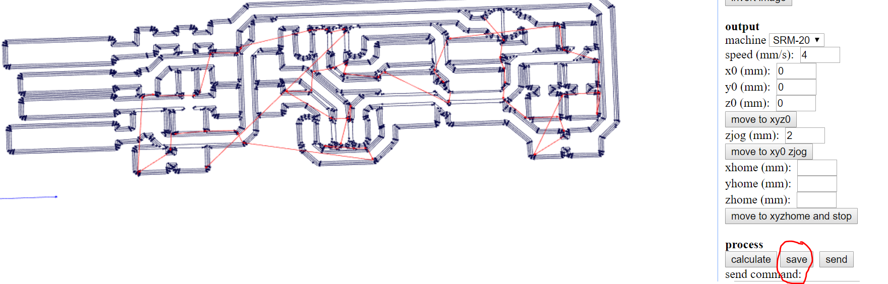
Step 3-Selecting the Process
Now select the process : Blue circled-Traces to cut the path, Red circled-To Cut the board outline to prey it out.
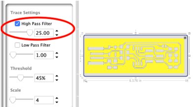
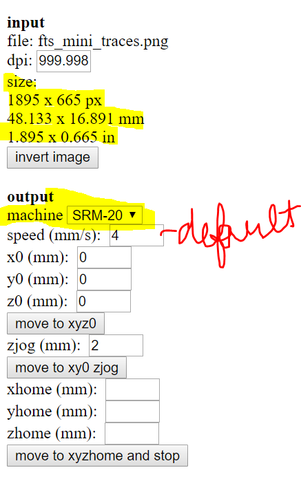
Step 4- Checking the size of image
On the right hand side toolbar check whetehr the dimensions of the image are correct and then select the Machine.
The by default speed is 4mm/sec we don't need to manipulate that.
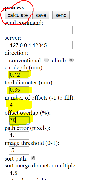
Step 5-Selecting the Process Parameters
After doing the group assignment and understanding the machine th conclusion of the parameters are displayed I used this settings for milling my board.
Step 5- generating tool path
After sCalculating mods will take some time to generate tool path depending on the process parameters given and after that you can just save your file and it will be saved in your downloads folder in.rml extension.
Understanding Our various parametrs and V-bit
Understanding Our fabmodules parameters- Optimum Settings Used
I used 0.12 as it worked best for out makeshift V-bit.
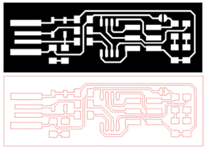
Download the traces and outline files from here-
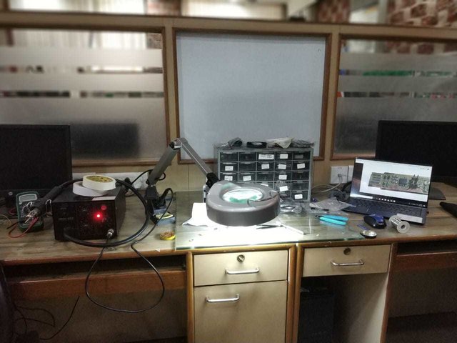
Let's Do the milling
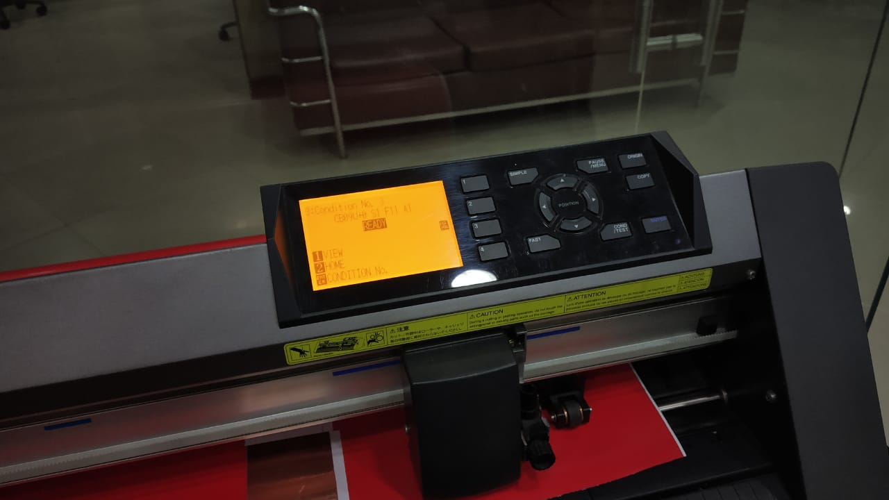
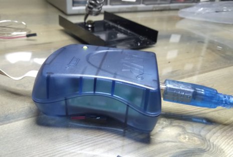
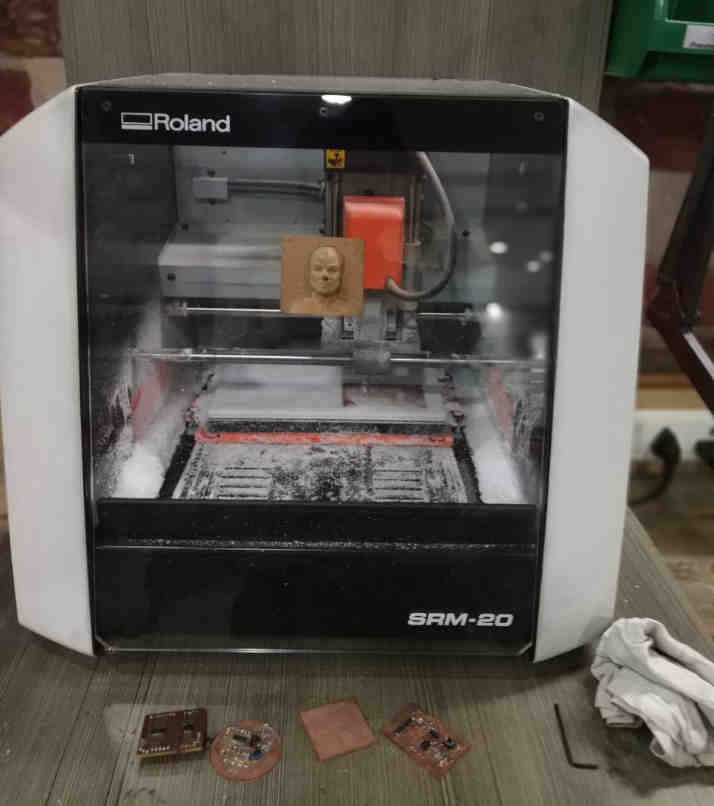
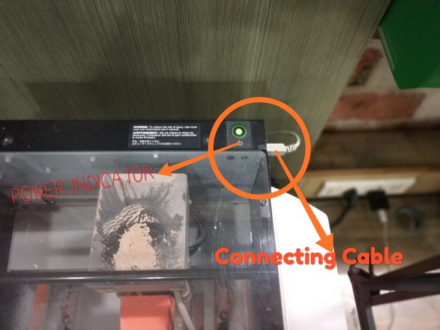
Software for operating the machine - V panel for SRM-20
The machine consit of a power button and a cable to connect to the PC in our lab a setup is made for SRM so I was saved from downloading any kind of software for it as it was already connected to lab's PC which had the software for it.
Using V panel to operate SRM
The video shows the movement of the tool using the gui of v panel.